Recap
In our last episode, I introduced Fritzing — a novice-friendly hardware design package that we are using to design a real time clock shield for an Arduino. We saw how we can use Fritzing to design the prototype for it on a breadboard. This time, we'll see how to take that breadboard prototype and generate a schematic design. Then — still using Fritzing — we’ll convert it into a printed circuit board (PCB) layout that we will have manufactured for us by SparkFun’s BatchPCB service.
One thing to remember while going through all this is that Fritzing is but one among many open source hardware design tools that let you draw schematics and generate PCB files. However, Fritzing is unique (as far as I know) in that it also lets you draw the circuit first on a breadboard that then automatically generates the schematic and PCB drawings.
For those of us who prototype with breadboards, this gives us not only an intuitive entry into the design, but it produces excellent drawings that we can use for documenting our projects. You’ll see lots of Arduino projects on the Internet that use Fritzing for documentation. It is the clarity that the Fritzing drawings give that make this tool so popular.
The Schematic
To get things rolling, the breadboard illustration from last month is shown in Figure 1.
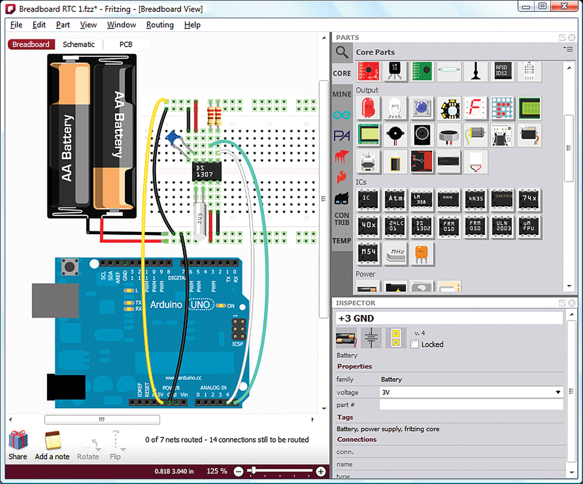
FIGURE 1. Real time clock on a breadboard.
The next thing you need to do is click on the Schematic button as shown in Figure 2.
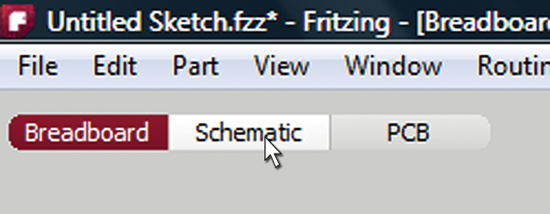
FIGURE 2. Select “Schematic.”
You’ll see the schematic window with the schematic version of the breadboard parts scattered about as shown in Figure 3.
FIGURE 3. The schematic, not yet wired.
Now, let’s move the parts to the positions that will facilitate adding the wires as shown in Figure 4.
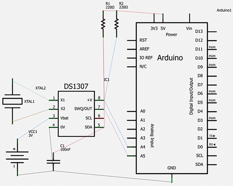
FIGURE 4. Reposition the parts.
Notice that as you move the parts around, tiny lines stick to the parts and stretch or contract a bit like a virtual rubberband. Those lines represent the part connections that you made in the breadboard. Similar to how you drew the wires on the breadboard, you use your mouse to grab a part connection point and stretch a line to the other end of the connection (refer to Figure 5).
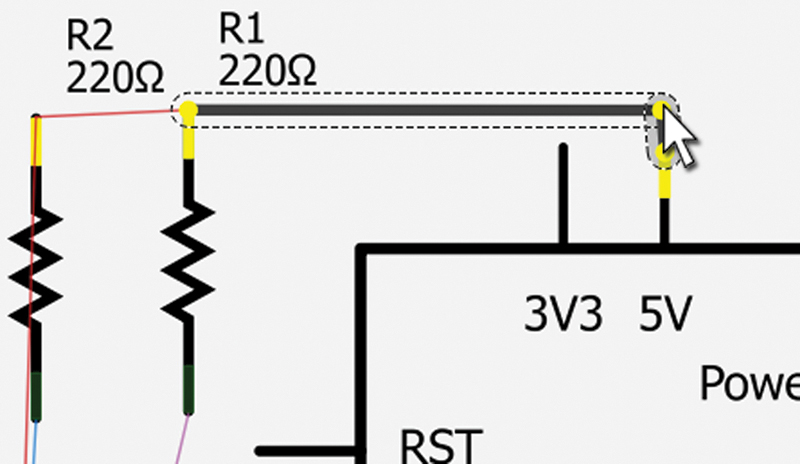
FIGURE 5. Adding a wire.
You may want to play around with this a bit, but keep in mind that your goal is not only to connect the parts, but to generate a schematic image that visually explains how the circuit is connected. This is not just about design; it is also about the very important and often underserved aspect of design: the documentation. To me, the image in Figure 6 represents a typical way to show a design in a schematic format.
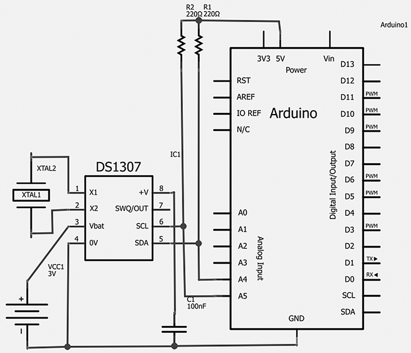
FIGURE 6. The schematic, all wired up.
The Printed Circuit Board Layout
To open the PCB layout window, click on the PCB button shown in Figure 7.
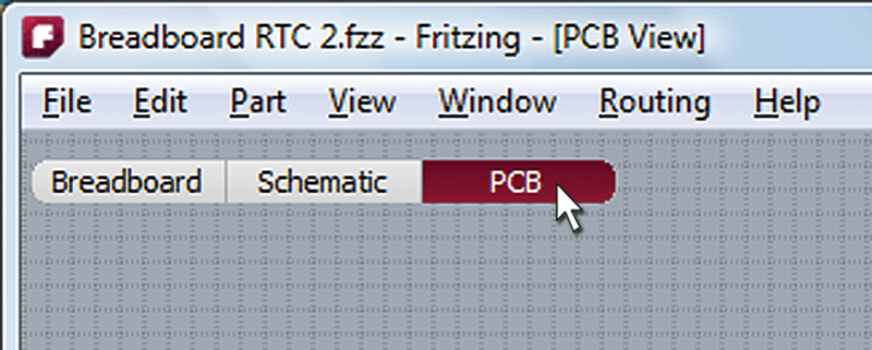
FIGURE 7. Select “PCB.”
You’ll get a raw layout something like what you see in Figure 8.
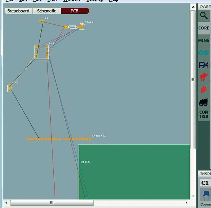
FIGURE 8. The raw PCB layout.
Your goal here is similar to what you did with the schematic: You want to move the parts on the PCB so that the layout makes sense. And by sense, in this case, I mean that the parts are easiest to connect with PCB ‘wires.’ This routing of the wires is a skill that comes with lots of practice where you try what seems most logical, then rip up (delete the wire) and retry until you get something that seems optimal to you.
In Figure 9, we see the parts placed on the corner of the default PCB.
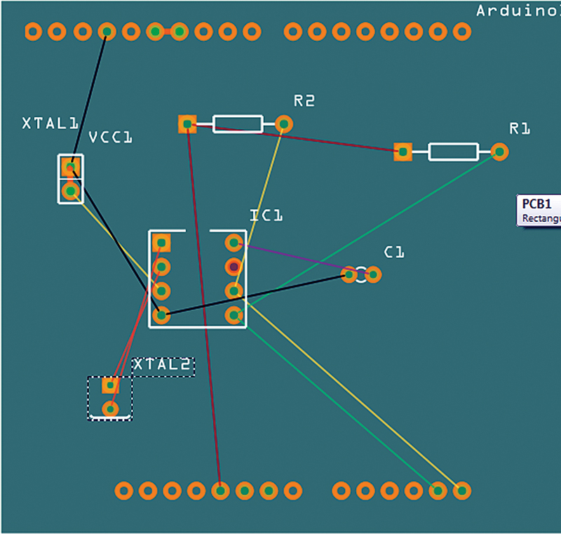
FIGURE 9. Moving parts to the board.
Obviously, the default PCB is too large so we want to adjust it, and then ...
It Crashed!
Oh, the humanity! The blood was ankle deep ... I WANT MY MONEY BACK! Oh wait ... this is free software in beta release, so I’ll just live with this minor inconvenience and move on. Although, this was a little more than a minor inconvenience. What I did was close my laptop to take somewhere with me and when I opened the laptop back up — NOTHING! Just a black screen and a forlorn arrow cursor that my mouse wouldn’t move.
So, I waited 10 minutes hoping the microspirits would work some magic ... but nothing. I removed the battery to reset it and after taking forever to completely reboot, I got the message in Figure 10 suggesting the Fritzing may have crashed.
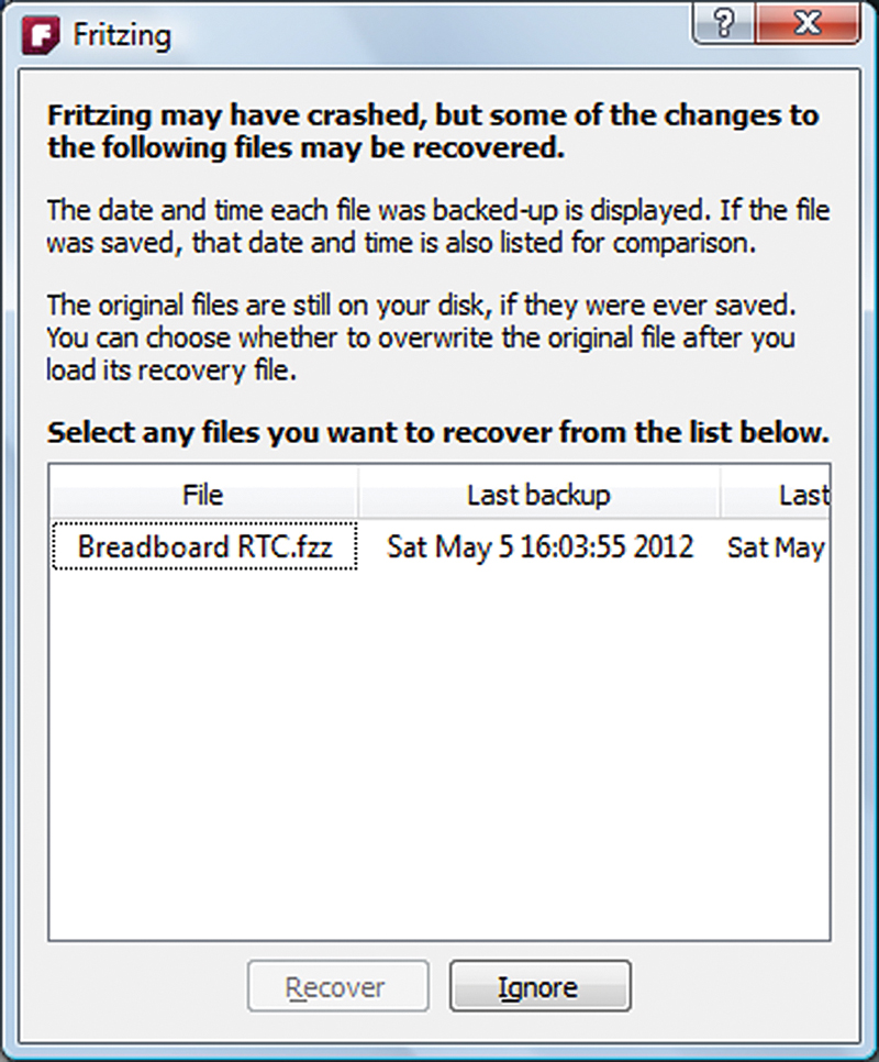
FIGURE 10. Fritzing may have crashed.
MAY HAVE!? I WANT MY MONEY BACK! (Okay, let’s take a deep breath, remember the price and that it is beta, and see what we can recover.)
I clicked on the .fzz file and followed the suggestions. I renamed the file just in case, and as luck would have it I was able to recover the work. (Yeah!) It took a while to get back in business, but again the price is right and frankly I’m having fun with Fritzing. One thing I noticed when recovering the file is that for some strange reason it was saving my work in the Windows downloads directory, so I created a new directory under C:\Fritzing\mySketches and moved my files there. (I had to leave again, but this time I closed Fritzing before closing my laptop.)
Next thing I did was resize the PCB to fit the Arduino pins so I can make this an Arduino shield, which is a PCB that plugs in on top of an Arduino. Next, we move the parts. Notice that you can move the parts anywhere, but that isn’t such a good idea when designing a PCB. In fact, you want to move parts to specific locations in relation to each other. Often, we have parts that have pins that are on 0.1” centers, so let’s set up a grid where parts can be moved around, and land on 0.1” points in relation to each other. We see in Figure 11 that we can check the “Align to Grid’ and ‘Show Grid’ selections in the View menu; we get the grid shown in Figure 12.
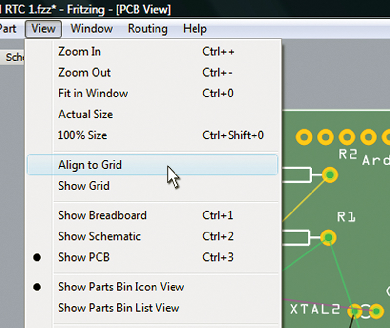
FIGURE 11. Align to Grid.
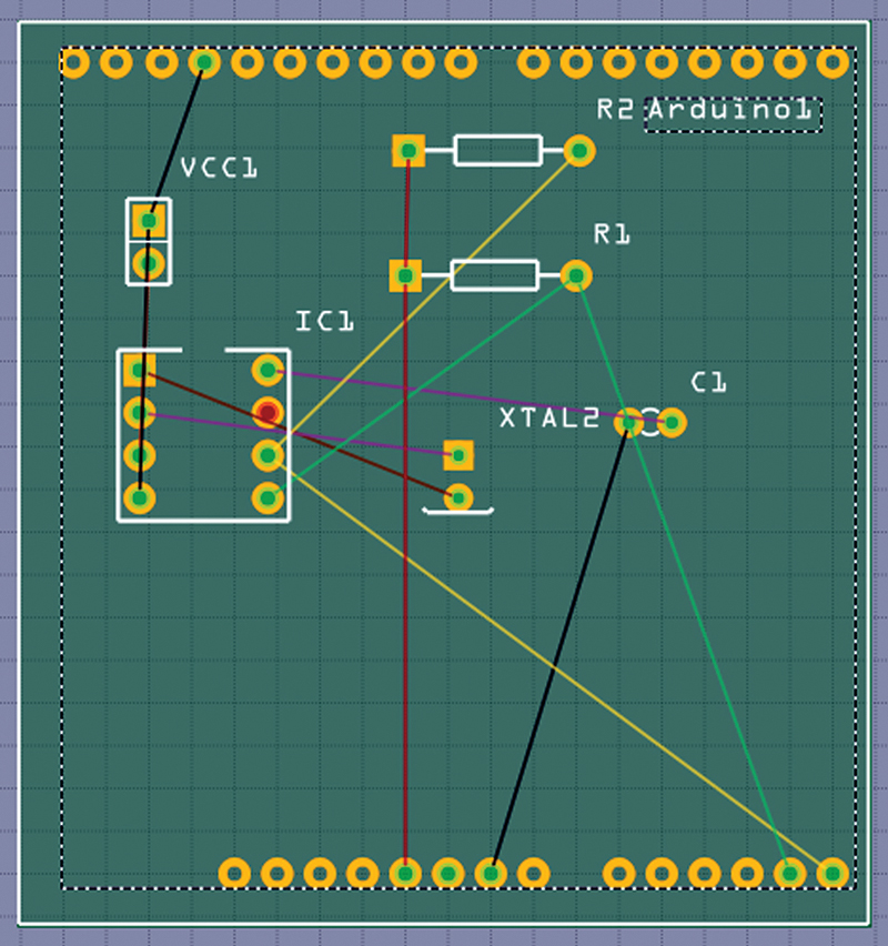
FIGURE 12. PCB parts on the grid.
Now, let’s move these parts to reasonable positions and add the wires. First thing you’ll notice is that every time you try to grab a part, you end up grabbing the Arduino! To prevent this, you right-click on the Arduino part, select ‘Lock Part,’ then click ‘Raise or Lower.’ Select the ‘Send to back’ option. Now you can move the other parts that are sitting on top of the locked Arduino layer.
In Figure 13, I’ve moved the parts to the lower right corner conveniently located to each other’s pins for wiring.
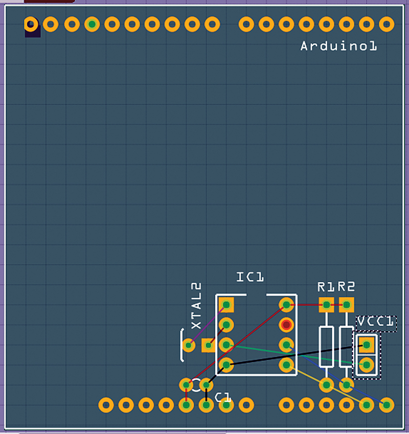
FIGURE 13. The PCB parts, moved.
The lines connecting the pins are called the rats nest (though I can’t imagine why) and they act like rubber bands, indicating where the PCB wires are to go. Your goal is to get the rats nest minimized so the wires can be as short as possible. Next, note that the battery terminal doesn’t have any indicator of which pin goes to GND and which goes to the +3 volt line of the battery, so I right-click on the VCC1 label for the part which gives me the window shown in Figure 14.
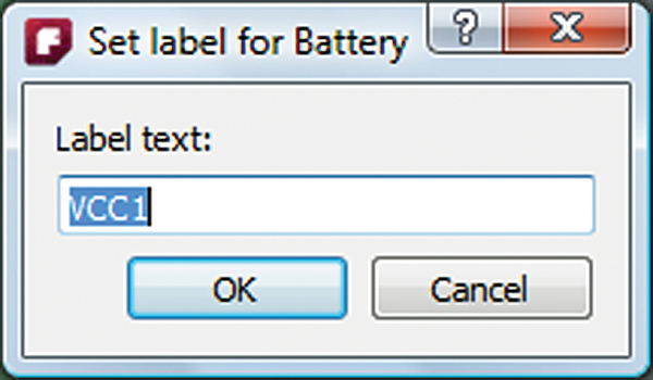
FIGURE 14. “Label text.”
I then change the VCC1 to ‘GND +3.’ I rotate the text and place it next to the connector as shown in Figure 15.
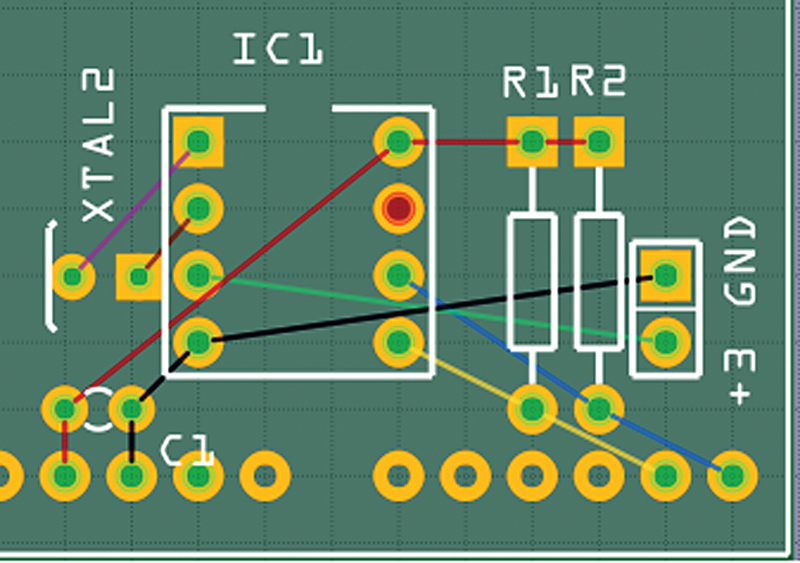
FIGURE 15. Ready to route the wires.
Fritzing has an auto-router, but we won’t use it since this is a very small board and I find routing is fairly intuitive. You just click on a pin and move the wire to the next connection and release it. Figure 16 shows what happened when I wired the VCC, GND, and crystal pins.
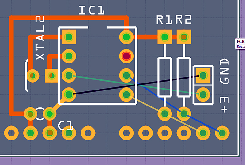
FIGURE 16. First attempt at wiring.
I then noticed something that I should have seen earlier (had I been paying attention). The battery wires will cross each other on their way to the DS1307 which would require either two layers or some funky routing. Also, the I2C wire on the left to R1 from the Arduino doesn’t have enough room to be routed. So, I flipped the battery terminal and moved the resistors up, and tried again.
In Figure 17, we see my first finished wiring attempt.
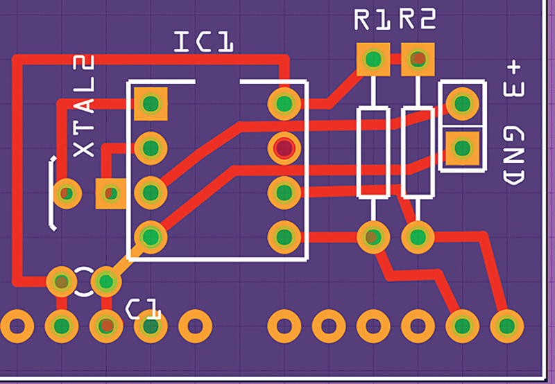
FIGURE 17. First finished wiring.
I couldn’t figure out how to change the grid size, so I shut it off and carefully routed the wires. As an experienced PCB designer, I immediately noticed something quite scary. Wires on a PCB are called traces. The traces and the pads on the right of the DS1307 look like they short out. In my experience, I can set the size of the traces and the parts pads so that I would normally be able to route a trace between IC pins, but it sure doesn’t look like that will work here. Will this mean that I’m going to have to use two layers so that I can drop those wires to the bottom, and route them up and over?
Well, let’s hope what Fritzing is showing us isn’t what it generates for the final PCB file. So, click on the ‘Export for PCB’ and the ‘Etchable (PDF)’ as shown in Figure 18.
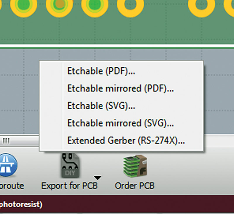
FIGURE 18. Export for PCB.
This gives us five PDF files — one for each layer. Let’s look at the ‘...etch_bottom_copper.pdf’ shown in Figure 19.
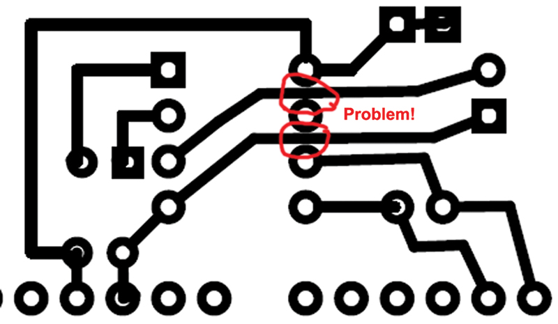
FIGURE 19. PCB — we have a problem.
See those red circles? Yes, we have a problem!
Okay, I’m used to being able to set the pad and trace dimensions, but Fritzing doesn’t seem ready for that. Let’s reroute the troubling traces on the opposite side and see what we get.
To fix this, we click on the problem traces and change the side from bottom to top as shown in Figure 20.
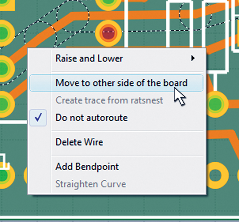
FIGURE 20. “Move to other side of the board.”
Then, reroute them up and over to the battery terminal BUT notice that we still have a problem since these traces will have to cross — unless we flip the battery terminal back like it was to begin with (sigh!). The results are shown in Figure 16. Yes, I could have shown all this in the correct order to begin with, but I think it is helpful to see the actual problems I ran into and how I fixed them. The resulting top and bottom layer are shown in Figure 21.
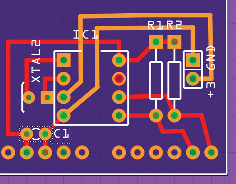
FIGURE 21. Is this the final wiring?
Actually, take a long hard look at Figure 21. Ask yourself if this is the final wiring or could you perhaps make some minor changes and get all the wires on one side of the board. Well, it’s possible, but since my goal here is to produce a PCB design that can be sent to a fab house (where someone else will do the work), we’ll just leave it.
I have to say that making a board with all that free space and the entire upper row of Arduino pins gives me the creeps — so much wasted space. Since we are making an Arduino shield we actually need all those pins so that we can — theoretically — mount another shield on top of the one we are making. [BTW, I found that you can — in fact — change the wire size in Fritzing! Just highlight the trace in question and you can change the width in the Inspector window Width dropdown box to 16, 24, 32, or 48 mils.]
Sending It Out to a PCB House
Fritzing has a feature that lets you get your board fabricated in Europe. For an Arduino shield, it costs $38 + shipping. Frankly, I’d like to see these guys get rewarded for their efforts (which would also give them incentive to improve their product), but I know there are much less expensive options for those of us in the US, so let’s take a look at one: SparkFun’s BatchPCB. Of course, there is always a down side for every choice. BatchPCB is cheaper but it takes longer to get the board (to the US, 3-10 days for Fritzing; 3+ weeks for BatchPCB).
I chose BatchPCB to fabricate this board since it is relatively cheap and easy to work with. Be aware though that none of the fab houses are exactly novice friendly and you have to eat your mistakes. Fortunately, making mistakes and living with the consequences is one of the best ways to learn.
PCB fab houses require files in certain specific formats. We’ll use the Gerber format supported by Fritzing. Notice that the Fritzing ‘Export for PCB’ has an ‘Extended Gerber (RS-247X)...’ option, so let’s go with that. This generates the following files:
Breadboard RTC 1_contour.gm1
Breadboard RTC 1_copperBottom.gbl
Breadboard RTC 1_copperTop.gtl
Breadboard RTC 1_drill.txt
Breadboard RTC 1_maskBottom.gts
Breadboard RTC 1_maskTop.gts
Breadboard RTC 1_silkTop.gto
Look at the Files in Viewplot
You can get Viewplot for free at www.viewplot.com. Click ‘File’ and ‘Load files,’ then navigate to the Gerber files in your Fritzing directory and load them.
You’ll get a couple of cryptic windows, but just click okay on them and you’ll see something like what is shown in Figure 22.
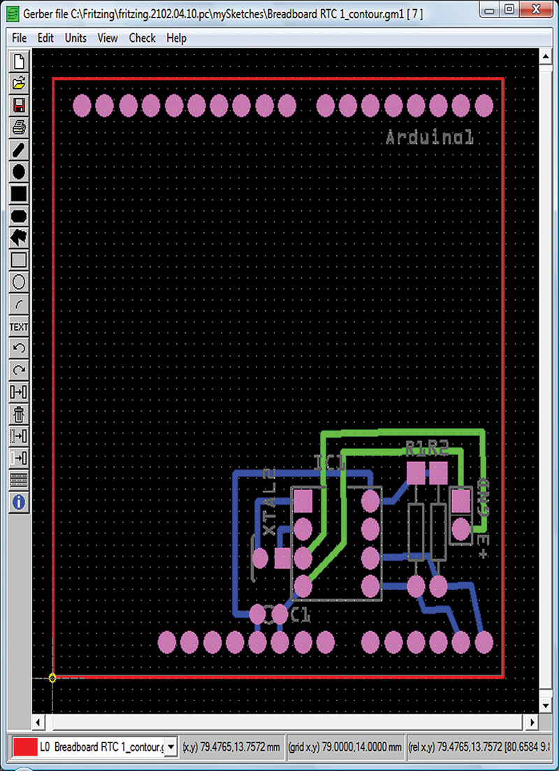
FIGURE 22. The RTC shield in Viewplot.
Viewplot gives you the opportunity to carefully inspect each layer before sending it to the fab house. I won’t go into the details on how to use Viewplot since it is fairly intuitive.
Our board is pretty simple and there doesn’t appear to be any potential problems, so let’s submit these files to BatchPCB and let them run them through some programs that look for common errors.
Onward to BatchPCB
Take a look around www.BatchPCB.com and get familiar with what they do. They have lots of stuff to help you. Let’s put all our Gerber files into a single zip file that we’ll call Breadboard_RTC.zip. Click on the ‘Upload New Design,’ then name the design and upload the zip file. To use their service, you must rename some of your files. Rename ...drill.txt to ...drill.drl and ...contour.gm1 to ...contour.oln.
BatchPCB uploads the files and shows you an image of each layer; Figure 23 shows the bottom copper layer.
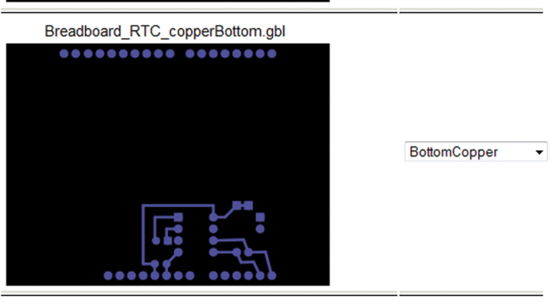
FIGURE 23. BatchPCB bottom copper image.
They will then provide you with board statistics. The important one here is that the board is 4.25 square inches; they charge by the square inch which, in this case, will be $10.62 — not too bad.
They also generate pictures similar to what we saw in Viewplot. (Figure 18 shows the bottom copper layer.) Finally, BatchPCB generates a picture for you to order from as shown in Figure 24.
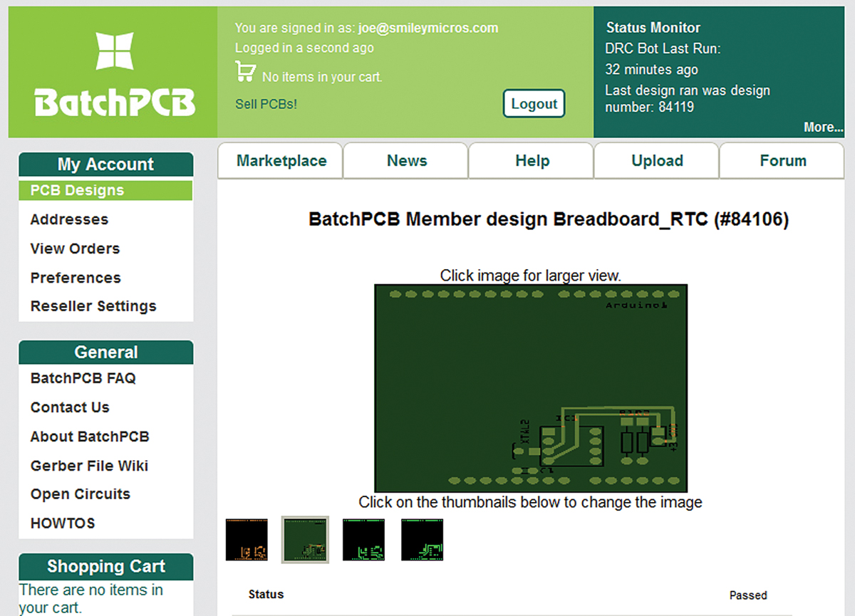
FIGURE 24. BatchPCB ready to build.
Well, $10.62, plus $10.00 for handling, plus $5.65 for shipping so $26.27. I could order more at $10.62 each and the handling charge and shipping stay about the same so each additional one is proportionally less, but one will do for this learning exercise so one is enough.
[BTW — you can get boards much cheaper from China, but it is also more complex so we’ll reserve that option for a later Workshop.]
Now We Wait ...
BatchPCB works — as its name implies — in batches. That is, it waits till it has a big enough batch of boards to fill a PCB panel. It then gets sent to Gold Phoenix in China who makes the full panel, then cuts out all the boards in that batch.
This process takes an unknown amount of time since your board might be the last one on the panel so it gets sent off quickly, or the first on the next panel meaning it has to wait.
So, how long will we have to wait? Stay tuned and find out. NV
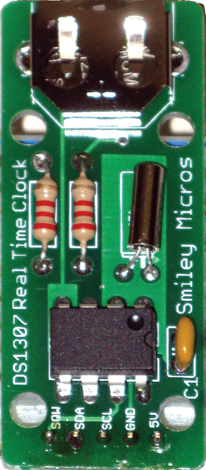
FIGURE A. The DS1307RTC kit.
These two parts of the Fritzing tutorial show you how to design and build your own DS1307 based real time clock, but if you just want one to play with, you can purchase the DS1307RTC kit from the Nuts & Volts webstore, which contains all the parts you’ll need including a PCB (better than the one we designed here) that we discussed in workshop 48.