Timer ICs are designed to generate accurate and stable C-R — defined timing periods, for use in monostable ‘one-shot’ pulse generator and free-running astable squarewave generator applications. The best known timer ICs are the ‘555’ family of devices, which are available in both single (555) and dual (556) bipolar packages and also in CMOS forms (7555 and 7556); they use a mixture of linear and digital IC technology. This article explains 555 basics and shows ways of using the IC in monostable applications.
555 BASICS
The 555 is a versatile timer IC that generates stable timing periods from a few microseconds to hundreds of seconds via a simple C-R network, and gives good output waveforms with typical rise and fall times of 100ns. When used in the monostable mode, its output can be pulse-width modulated (PWM) and, in the astable mode, it can be subjected to frequency-sweep control, to frequency modulation (FM), or to pulse-position modulation (PPM). Figures 1 to 3 give basic outline and performance details of the bipolar 555 and 556 ICs and their CMOS counterparts, the 7555 and 7556.
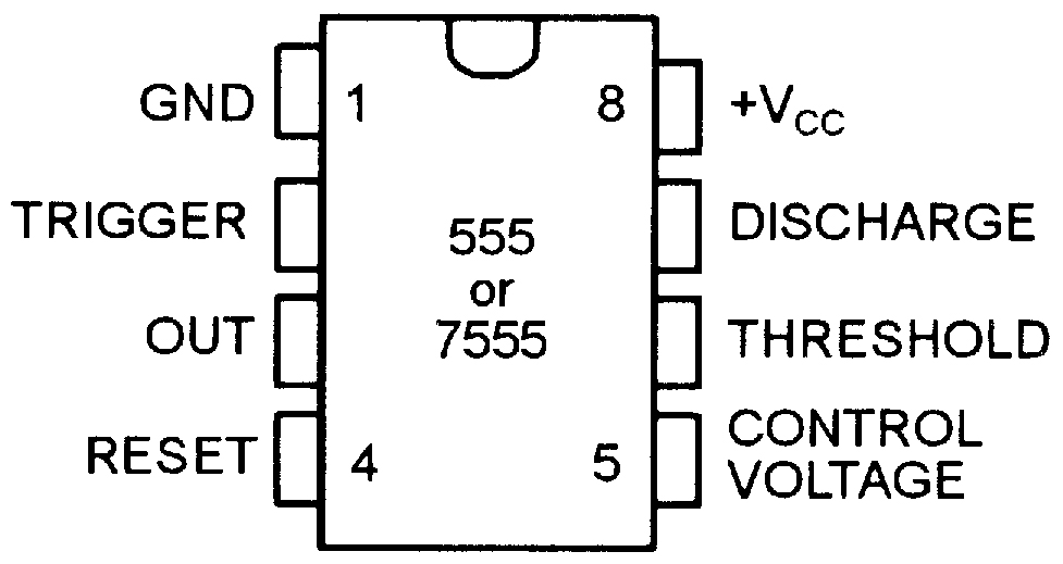
FIGURE 1. Outline and pin notations of the eight-pin DIL versions of the 555 (or 7555) timer IC.

FIGURE 2. Outline and pin notations of the 14-pin DIL version of the 556 (or 7556) ‘dual timer’ IC.
| Parameter |
Bipolar 555 |
CMOS 7555 |
| Power supply range |
4.5V to 16V |
2V to 18V |
| Supply current at Vcc = 15V |
10 mA |
0.1 mA |
| Output current, max. |
200 mA |
100 mA |
| Power dissipation, max. |
600 mW |
200 mW |
| Peak supply current transient |
400 mA |
10 mA |
| |
|
|
| Timing accuracy, drift with Vcc |
0.1%/V |
1%/V |
| Input current, trigger |
100 nA |
0.01 nA |
| Input current, threshold |
500 nA |
0.01 nA |
| Input current, reset |
100 µA |
0.02 nA |
| Output rise and fall times |
100 ns |
40 ns |
| |
|
|
| Minimum trigger-pulse width |
20 ns |
90 ns |
| Threshold voltage |
1/2 Vcc |
2/3 Vcc |
| Trigger voltage |
1/3 Vcc |
1/3 Vcc |
| Reset voltage |
0.7V |
0.7V |
FIGURE 3. Typical bipolar 555 and CMOS 7555 parameter values.
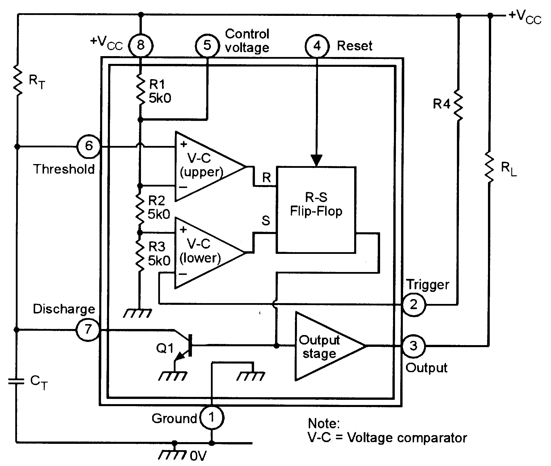
FIGURE 4. Functional block diagram (within the double lines) of the 555 timer IC, with external connections for use as a ‘timer.’
Figure 4 shows (within the double lines) the functional diagram of the bipolar 555 IC; the supply-driven 3 x 5k0 potential divider generates a 1/3 Vcc reference voltage on the non-inverting input of the lower voltage comparator and a 2/3 Vcc reference on the inverting input of the upper comparator. The comparator outputs control the R-S flip-flop which, in turn, controls the output stage and slave transistor Q1; the flip-flop state can also be controlled via pin 4. The diagram also shows the connections for using the 555 as a basic monostable multivibrator or timer, and the following explanation assumes that the IC is connected in this configuration.
When the Figure 4 timer circuit is in its quiescent state, pin 2 is held high via R4, Q1 is saturated and forms a short across timing capacitor CT, and pin 3 (output) is driven low. The monostable timer action is initiated by feeding a negative-going trigger pulse to pin 2, and as this pulse falls below the internal 1/3 Vcc reference, the output of the lower comparator changes state and switches the R-S flip-flop over, turning Q1 off and driving the pin 3 output high. As Q1 turns off, it removes the short from CT, which starts to charge exponentially via RT until eventually its voltage rises to 2/3 Vcc, at which point the upper comparator changes state and switches the R-S flip-flop over again, turning Q1 on and rapidly discharging CT and simultaneously switching output pin 3 low again, thus completing the operating sequence.
Note that, once triggered, this circuit cannot respond to additional triggering until the timing sequence is complete, but the sequence can be aborted at any time by feeding a negative-going pulse to RESET pin 4. The timing period, in which the pin 3 output is high, is given as
t = 1.1 x CT x RT,
where t is in ms (milliseconds), CT is in µF, and RT is in kilohms.

FIGURE 5. 555 time delays (t) for various values of RT and CT.
Figure 5 shows how delays of 10 µs to 100s can be obtained via CT and RT values in the range 1 nF (= 1000 pF) to 100 µF and 1k0 to 10M; CT must be a low leakage component. The timing periods can also be varied by applying a variable resistance or voltage between ground and the pin 5 CONTROL VOLTAGE terminal of the IC; this facility enables the periods to be externally modulated or compensated.
555 OR 7555?
All practical circuits shown in this article are designed around the standard bipolar 555 IC but, in most cases, will work equally well (or better) with a 7555 or similar CMOS version of the timer IC. Here are a few notes on the relative merits of the inexpensive bipolar 555 IC and its more expensive CMOS cousin, the 7555. The 555 is very popular, but cannot use supplies below 4.5V and typically draws 10 mA of quiescent current when operating from 15V. Worst of all, it draws a brief (a fraction of a microsecond) but massive 400 mA spike of supply current as its output transitions from one state to the other, and this generates an RF noise burst that can play havoc with nearby digital circuits. In critical 555 applications, this RF burst can be suppressed by wiring an electrolytic capacitor (10 µF to 100 µF) directly between supply pins 8 and 1.
The 7555 CMOS device suffers from none of these snags; it can use supplies in the range of 2V to 18V, draws only 100µA quiescent from a 15V supply, and draws a peak spike current of only 10 mA when its output transitions from one state to the other, thus generating negligible switching RFI.
Figure 3 shows a rationalized comparative summary of the 7555 and 555 characteristics. Note, on the debit side, that the 7555 performance is inferior in terms of drift-with-voltage accuracy, in some pulse-trigger characteristics, and in its output current drive and power dissipation capabilities (the 7555 output can typically sink a maximum of 100 mA but can source only 10 mA).
Note that some ‘low-power 555-type’ ICs (such as the TS555CN) use CMOS rather than bipolar technology; these ICs draw a very low supply current. Finally, remember that dual versions of both the 555 and 7555 are available in 14-pin DIL IC packages; the dual 555 is known as the 556, and the dual 7555 is known as the 7556.
PRACTICAL 555 TIMER CIRCUITS
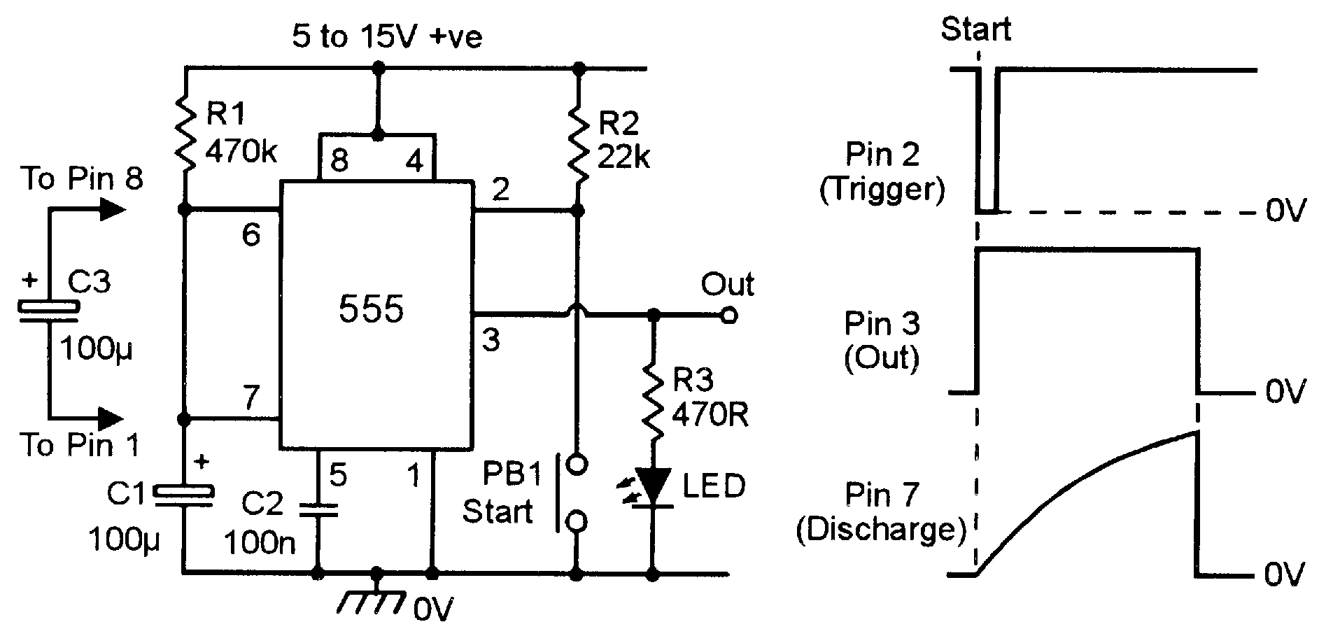
FIGURE 6. Circuit and waveforms of a simple 50s timer, with optional RFI suppression via C3.
Figure 6 shows a practical fixed-period (about 50s) manually-triggered 555 timer and its circuit waveforms. It is similar to Figure 4 except that the timing action is initiated by briefly closing START switch PB1, that pin 5 is decoupled via C2, and that the output state is visible via an LED. The fixed-period output pulse (set via R1-C1) is available at pin 3, and a high-impedance exponential sawtooth is available at pin 7. The circuit has optional RF suppression provided via C3.

FIGURE 7. 1.1s to 120s timer with RESET facility.
Figure 7 shows how the timing period of the basic Figure 6 circuit can be made variable from 1.1s to 120s by replacing R1 with a series-wired 10k fixed and 1M0 variable resistor, and how a RESET facility can be added to the circuit, enabling the timing period to be aborted at any moment.
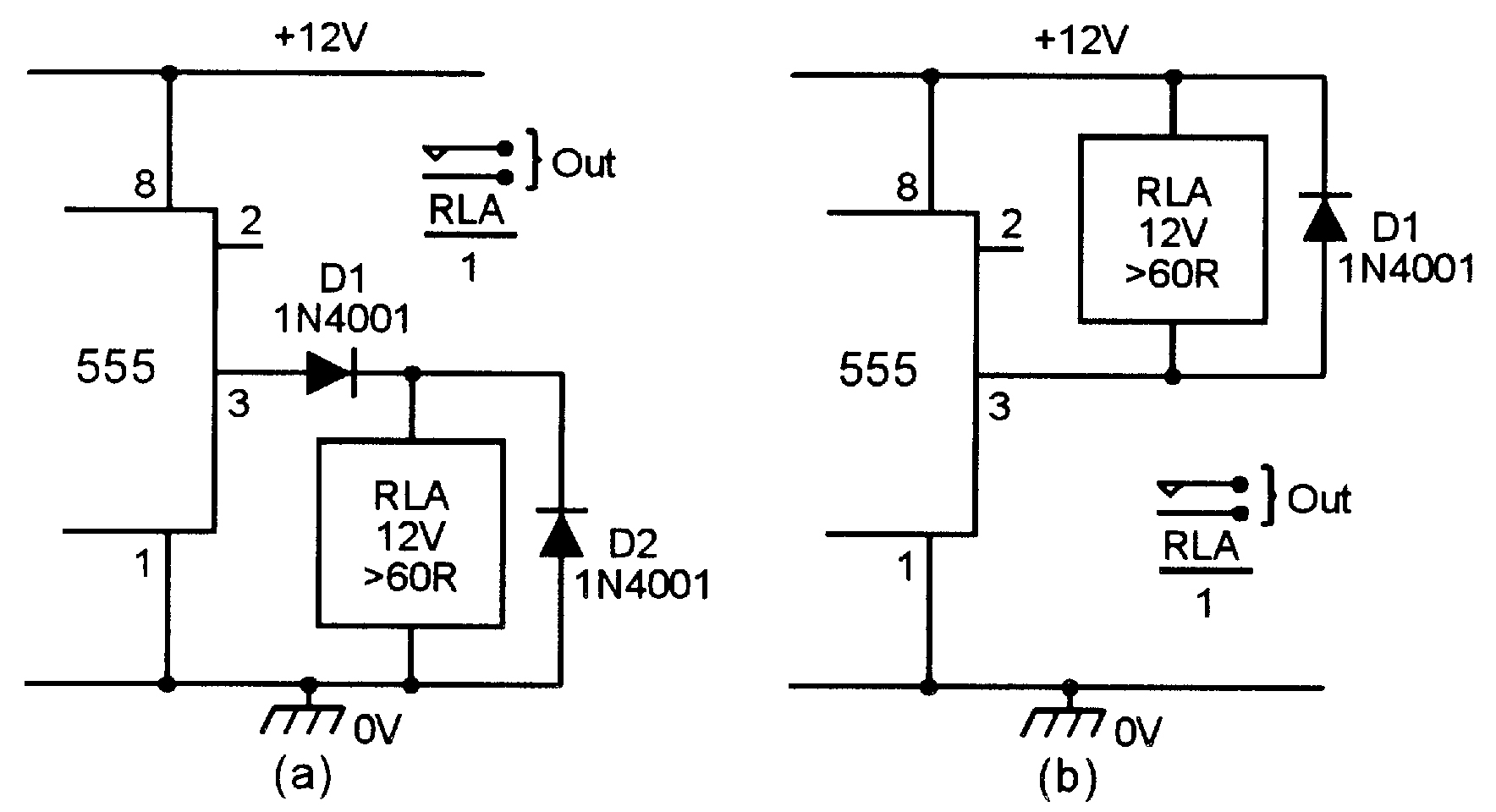
FIGURE 8. Alternative ways of driving a relay from the output of a 555.
The 555 can directly drive non-inductive loads (via pin 3) at currents up to 200 mA, but if relay coils or other inductive loads are used, the connections of Figure 8 must be used; the diodes protect the IC against inductive-switching damage. In Figure 8(a), the relay is normally off, but goes on while pin 3 is high during the timing period. In Figure 8(b), the relay is normally on, but turns off during the timing period.
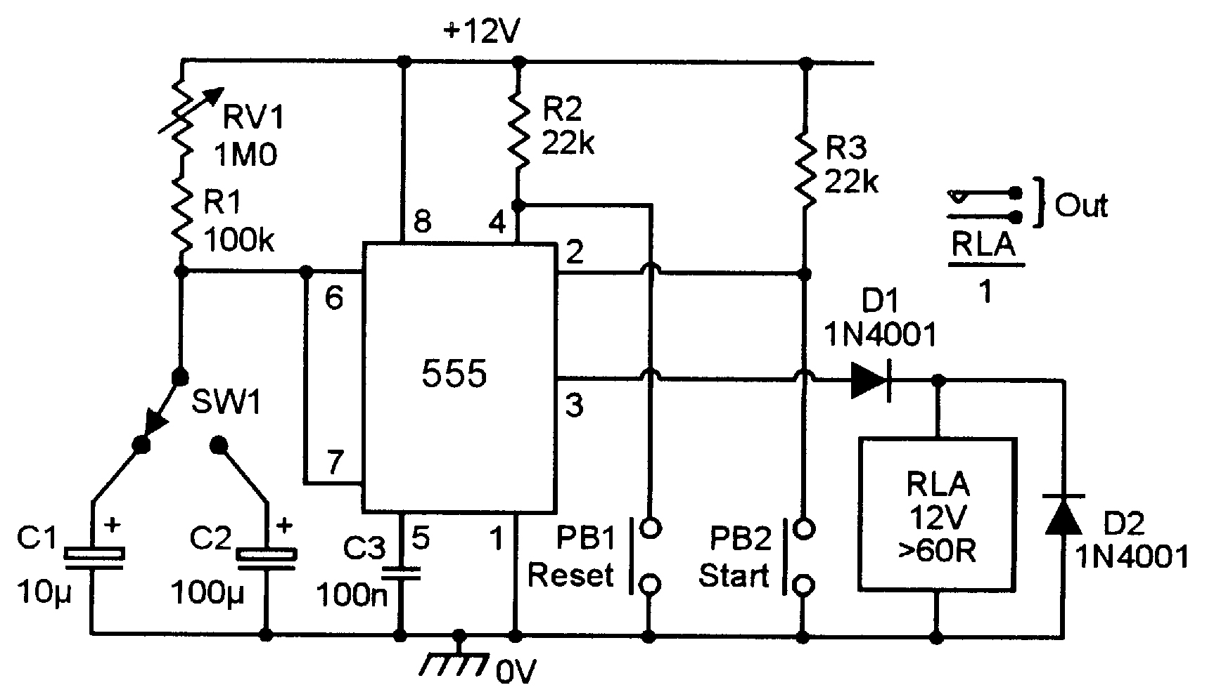
FIGURE 9. Simple two-range, 1.1s to 120s, relay-output timer.
Figure 9 shows a relay-output timer that spans 1.1s to 120s in two decade ranges. This is a useful general-purpose circuit, but consumes current even when the timer is in the ‘off’ mode, and its two RV1 scales must both be calibrated, since timing capacitors C1 and C2 are wide-tolerance electrolytic types. Figure 10 shows how these two defects can be overcome.
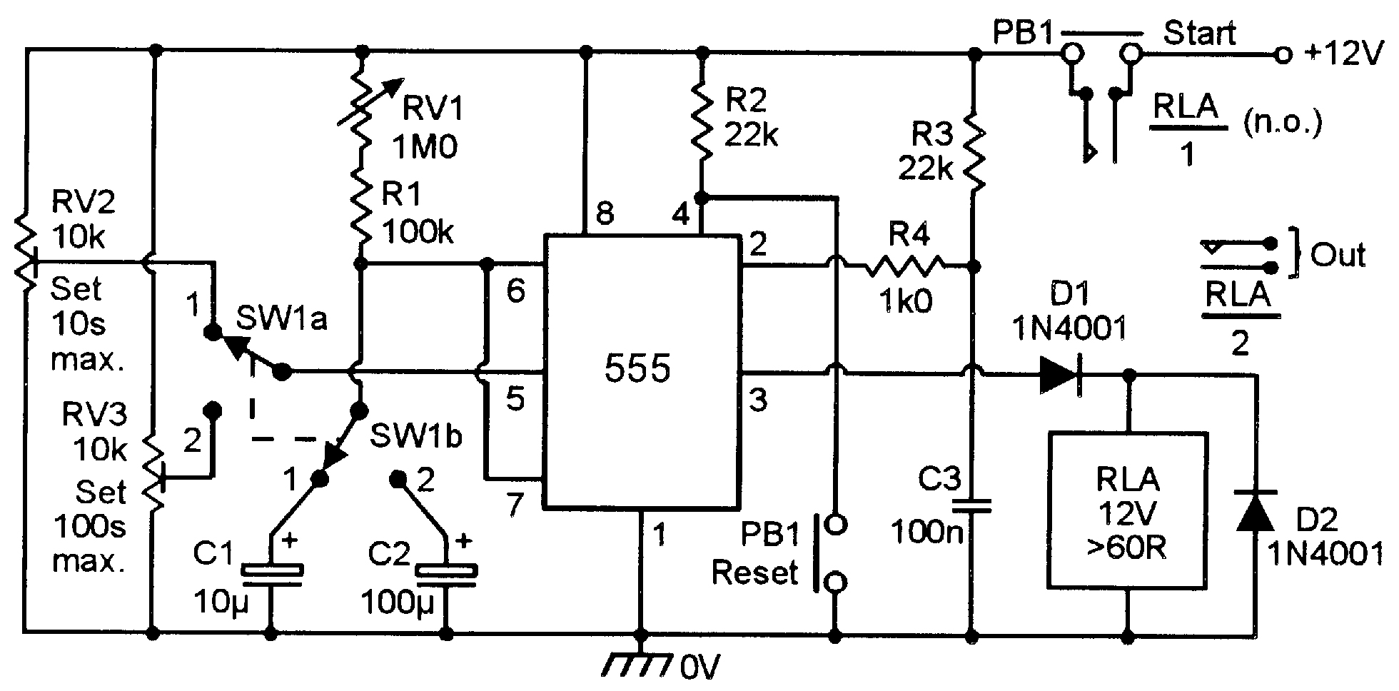
FIGURE 10. Precision (compensated) two-range (0.9s-10s, 9s-100s) timer.
Power is fed to the Figure 10 timer via PB1 or relay contacts RLA/1, which are normally both open. The timing cycle is started by briefly closing PB1, thus connecting power to the circuit. Initially, C3 is fully discharged and thus feeds a start pulse to the 555’s pin 2 via R4, thus starting the timing cycle and driving relay RLA on and closing RLA/1’s contacts, which then maintain the circuit’s power connection even when PB1 is released.
At the end of the timing cycle, the relay turns off again and contacts RLA/1 re-open, thus removing the circuit power again. The circuit’s timing is controlled mainly by R1-RV1 and by C1 or C2, but is also influenced by the settings of RV2 and RV3, which connect to pin 5 of the IC and enable the timing to be ‘trimmed’ so that the two timing ranges can use a single calibrated scale, even though wide-tolerance timing capacitors are used.
To initially set up the Figure 10 circuit, first set RV1 to maximum value, set range switch SW1 to position ‘1,’ activate START button PB1, and trim RV2 to give a timing period of precisely 10s. Next, set SW1 to position ‘2,’ activate PB1, and trim RV3 to give a timing period of 100s. Adjustments are then complete, and the timing scale can be calibrated over the full ‘10s’ range.

FIGURE 11. Automatic delayed-turn-off headlight control system for cars.
Figure 11 shows an automatic delayed-turn-off headlight control system for use in automobiles; it holds the headlights on for a pre-set period after the car is parked, thus illuminating a pathway, etc.; it does not interfere with normal headlight operation under actual driving conditions. It works as follows.
When the ignition switch is on, RLA is driven on via D3, and contacts RLA/1 are closed, connecting the 12V supply to both the timer circuit and the headlight switch. The headlights thus operate in the normal way under this condition, but C2 is fully discharged. When the ignition is first switched off, the relay tries to open, but at that instant, a negative trigger pulse is fed to the timer via C2 and initiates a 50s timing cycle that feeds current to the relay coil via D2, thus maintaining RLA/1’s connection to the headlight switch for 50s after the ignition is turned off. At the end of this period, RLA turns off and contacts RLA/1 open, breaking the supply connection to the timer circuit and the headlight switch, and the operation is complete.

FIGURE 12. Manually-triggered delayed-turn-off light control system for cars.
The above mode of circuit operation is compatible with most modern vehicles, in which the headlight switch is fed via the ignition switch. On older types of vehicles — where headlight operation is independent of the ignition switch — a manually-triggered delayed-turn-off headlight or spotlight control facility can be obtained by using the circuit in Figure 12. The action here is such that, if the vehicle has its lights off, they can be turned on for a pre-set 50s period by briefly pressing a START switch.
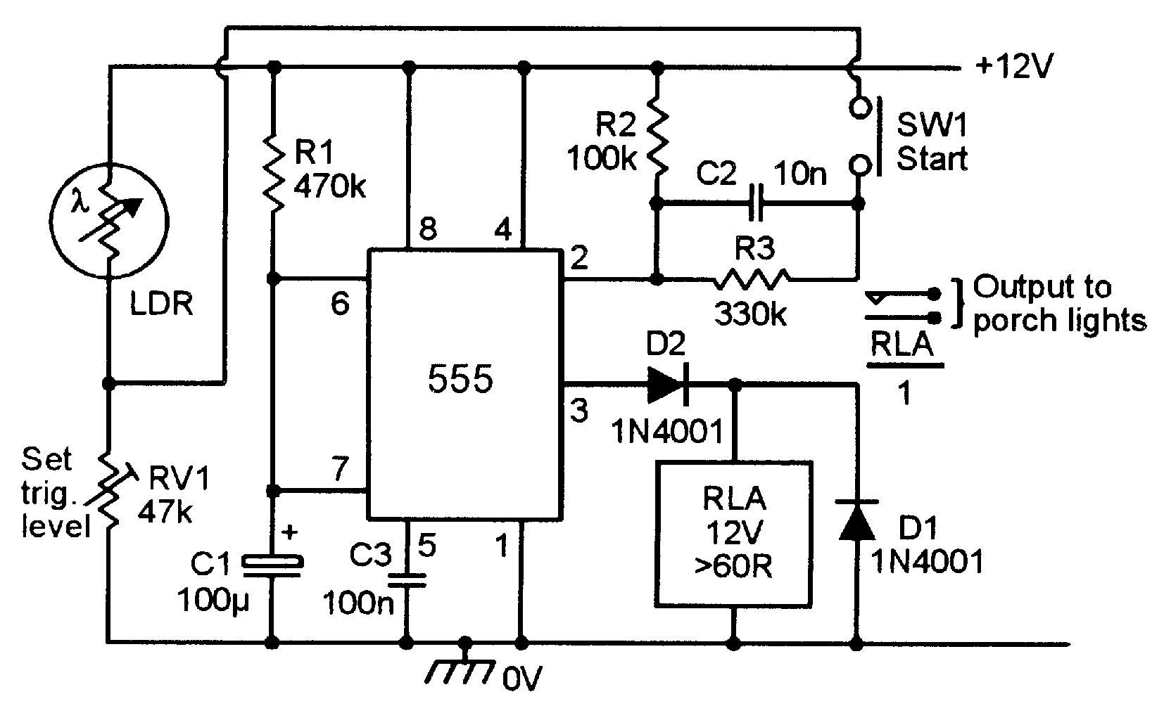
FIGURE 13. Automatic porch light turns on for a pre-set period only when triggered at night.
To complete this look at ‘timer’ applications of the 555 IC, Figure 13 shows a ‘smart’ timer that automatically turns a porch light on for 50s when the presence of a visitor is detected, but does so only under dark conditions. The visitor’s presence is detected via SW1 (a micro-switch activated by a porch gate, or a pressure-pad switch activated by body weight), and the dark condition is detected by a cadmium-sulphide light-sensitive resistor (LDR).
Circuit operation relies on the fact that timer triggering can only occur if the IC’s pin 2 trigger pulse falls below the ‘1/3 VCC’ value, and in Figure 13, the pulse is generated by closing SW1, but the pulse magnitude is controlled by the LDR-RV1 potential divider and depends on light level. Under bright conditions, the LDR-RV1 junction voltage is high, so effective trigger pulses cannot be generated, but under dark conditions, the LDR-RV1 junction voltage is low, and effective trigger pulses are generated each time SW1 is closed. The LDR needs a resistance in the range 1k0 to 47k at the required minimum ‘dark’ turn-on state, and RV1 sets the minimum ‘dark’ level at which the circuit will trigger.
PULSE GENERATOR CIRCUITS
The 555 can be used as a pulse generator by feeding suitable trigger signals to pin 2; it can generate good pulses with periods from 5 µS upwards; its maximum useful pulse repetition frequency is about 100 kHz. Pin 2 trigger signals must be negative-going pulses with amplitudes that switch from an OFF value above 2/3 VCC to an ON value below 1/3 VCC (triggering actually occurs as pin 2 drops below 1/3 VCC), and their width must be greater than 100 nS, but less than that of the desired output pulse.
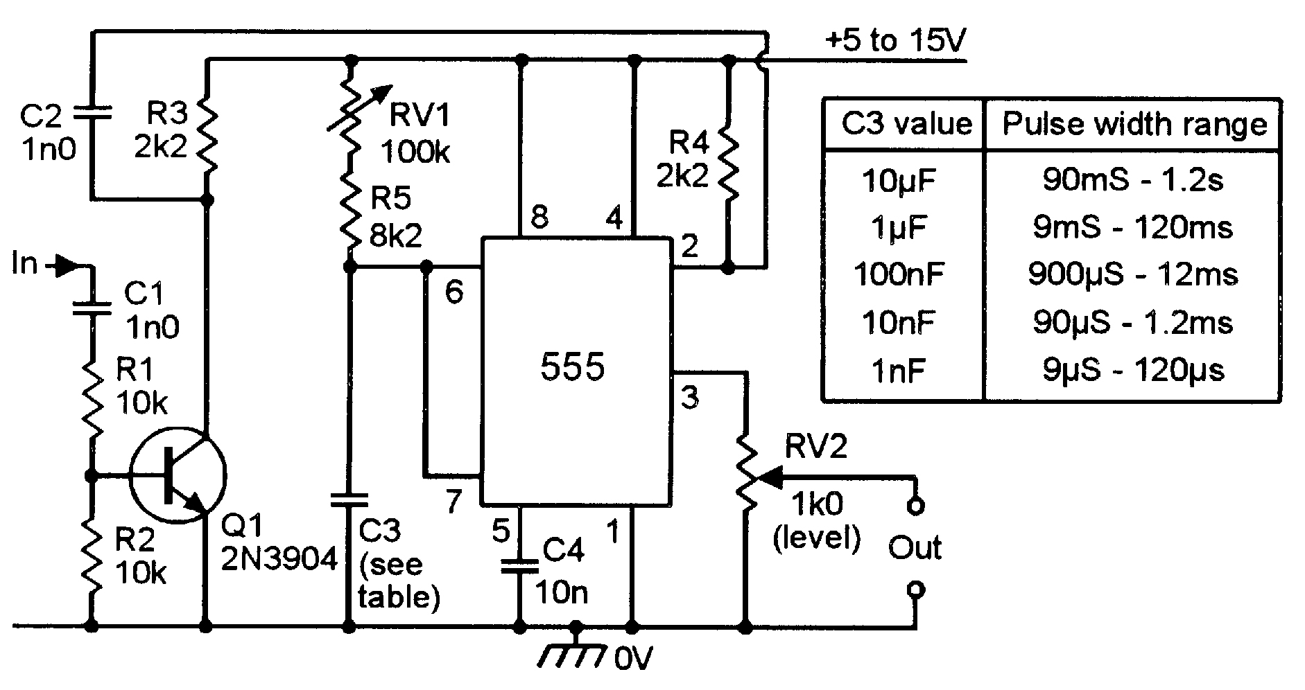
FIGURE 14. Simple add-on pulse generator is triggered by rectangular input signals.
Figure 14 shows a practical pulse generator that is triggered via rectangular input signals and can be used as an ‘add-on’ facility with an existing waveform generator. Q1 converts the input signal into one that switches fully between the supply-rail values, and this is differentiated into an appropriate trigger-pulse form via short time-constant network C2-R4 and fed to pin 2 of the 555. Variable-amplitude output pulses are available via RV2, and their widths are variable over a decade range via RV1, and can be switched in decade ranges by using the C3 values shown in the table. The total pulse width range spans 9 µS to 1.2s. C4 enhances circuit stability.
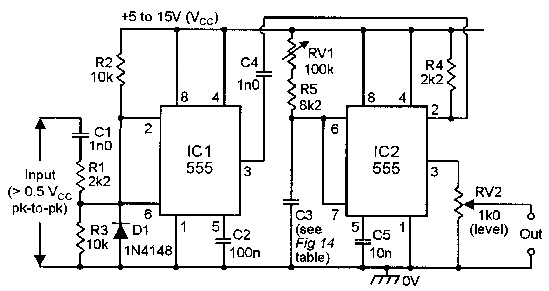
FIGURE 15. Improved add-on pulse generator is triggered by any input waveform.
Figures 13-15 show the circuit modified so that it can be directly driven by any type of input, including a sinewave; IC1 is wired as a Schmitt trigger and converts all inputs into a rectangular form that drives the IC2 monostable in the same way as described above. This circuit can be used as an add-on pulse generator in conjunction with any free-running generator that gives peak-to-peak outputs greater than 1/2 VCC.
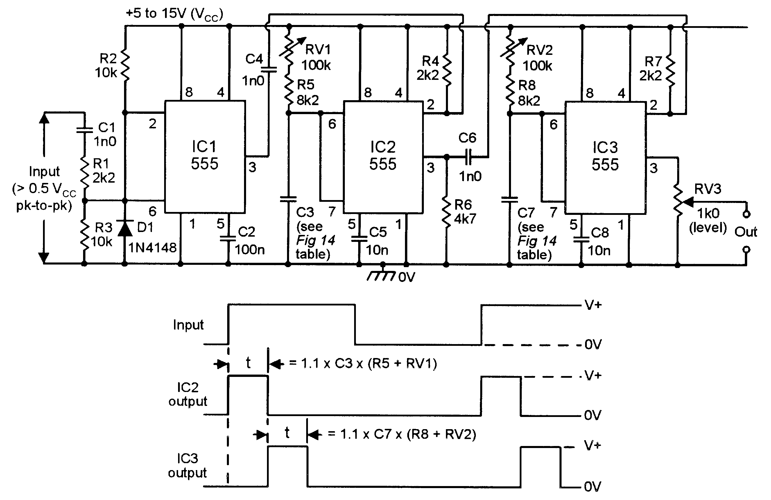
FIGURE 16. Add-on delayed-pulse generator is triggered by any input waveform.
To complete this look at 555 pulse generator circuits, Figure 13-16 shows three 555 ICs used to make an add-on delayed-pulse generator in which IC1 is used as a Schmitt trigger, IC2 is a monostable that is used to control the pulse’s delay width, and IC3 is used as the final pulse generator. The final output pulse appears some delayed time (set via IC2) after the application of the initial input trigger signal.
ANALOG FREQUENCY METERS
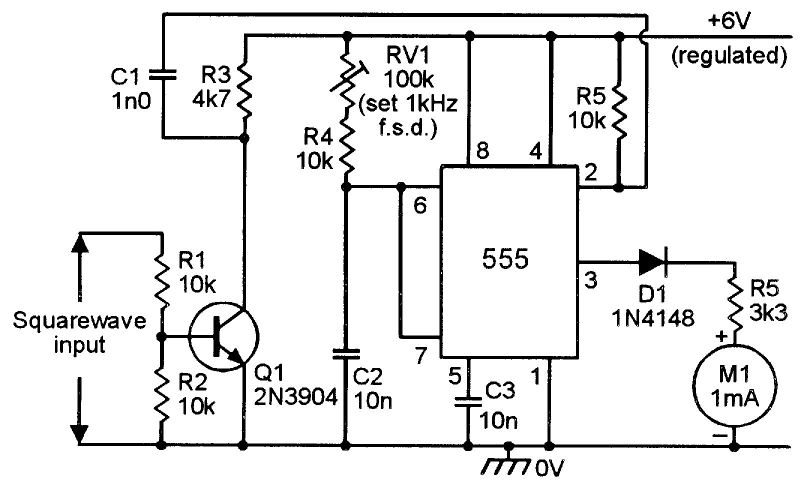
FIGURE 17. Simple 1 kHz linear-scale analog frequency meter.
One special application of the 555 pulse generator is as an analog meter driver that gives a direct reading of frequency, as in Figure 17. The IC’s pulse output is fed to 1 mA FSD moving-coil meter M1 via multiplier resistor R5 and offset-cancelling diode D1. The meter responds to the MEAN voltage of the pulse waveform (integrated over several trigger cycles), which is directly (linearly) proportional to input frequency. With the component values shown, this circuit reads 1 kHz FSD (set via RV1); other FSD values (from 100 Hz to 100 kHz) can be obtained by using alternative C3 values. The meter can be made to read frequencies up to 10s of MHz by feeding the input signals to the 555 via a digital divider.
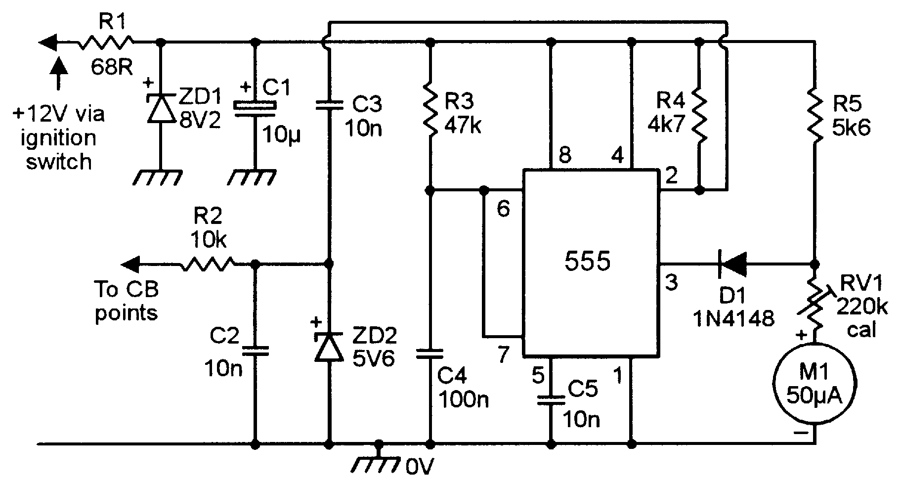
FIGURE 18. Car/motorcycle tachometer circuit.
Figure 18 shows the circuit modified as an analog tachometer (RPM meter) for use in cars or motorcycles. It is powered by a regulated 8V2 supply (derived via the ignition switch) and is triggered by the vehicle’s contact breaker (CB) points via the R2-C2-ZD2 waveform-conditioning network. The circuit action is such that current is applied to the 50 µA FSD meter via R5-RV1 and the IC supply line when the IC output is high, but is reduced to near-zero (via D1) when the output is low.
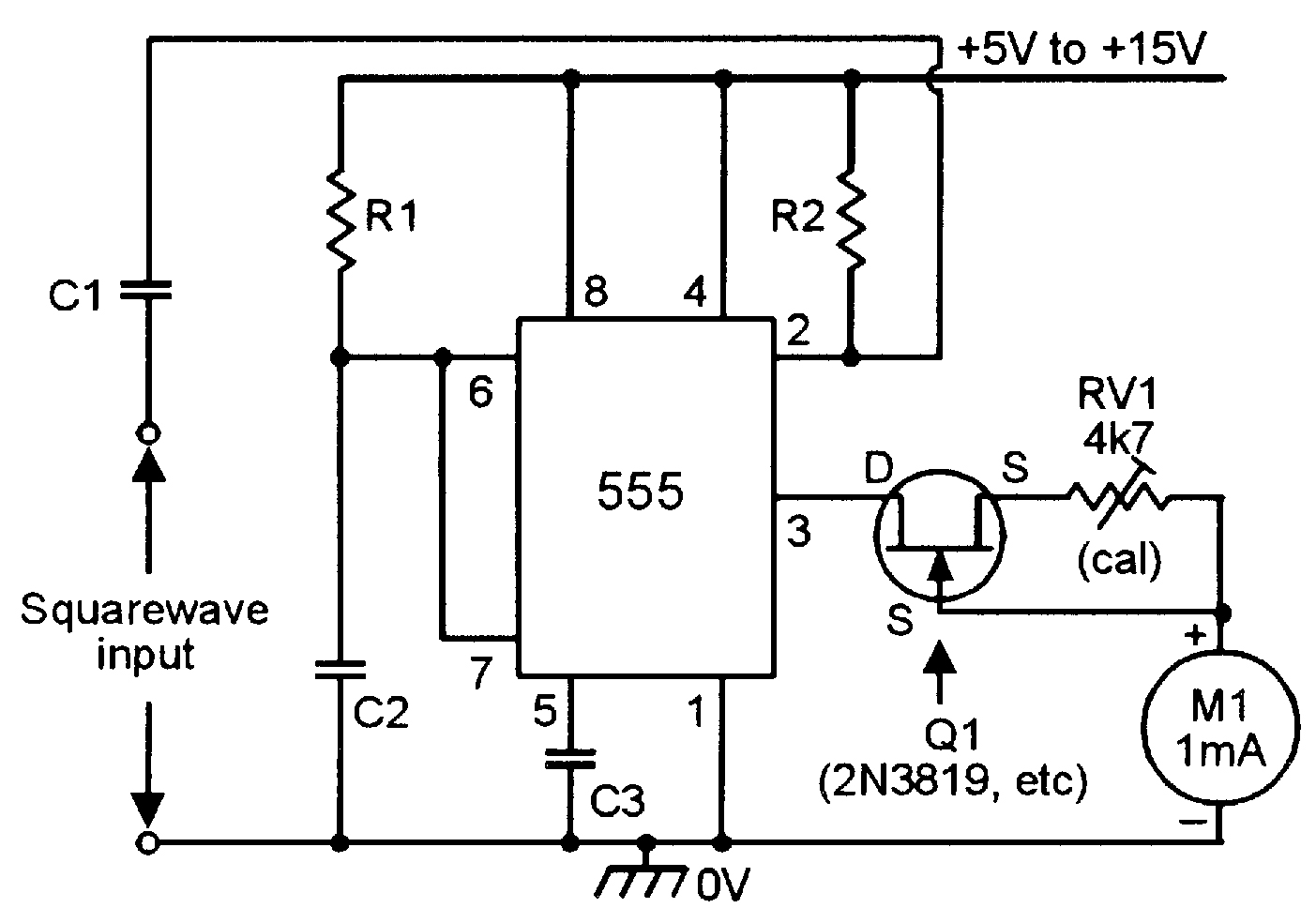
FIGURE 19. Alternative version of the analog frequency meter.
The Figure 17 and 18 circuits use regulated supply lines, to ensure constant pulse amplitude and thus a stable reading accuracy in the meter, which is used as a voltage indicator via the use of suitable ‘multiplier’ resistors. Figure 19 shows (in basic form) an alternative way of making an analog frequency meter, by feeding the 555’s output to the meter via JFET transistor Q1, which is wired (via RV1) as a constant-current generator, and thus feeds a fixed-amplitude pulse into the meter, irrespective of variations in supply line voltage, etc.
MISSING-PULSE DETECTOR
Finally, Figure 20 shows an event-failure alarm or ‘missing-pulse’ detector, which operates a relay or LED if a normally recurrent event fails to take place. The 555 is wired as a normal pulse generator, but Q1 is wired across timing capacitor C1 and is driven via trigger pin 2, which is fed with a series of brief pulse- or switch-derived clocking signals from the monitored event. The R3-C1 values are chosen so that the 555’s monostable period is slightly longer than the repetition period of the clock input signals.
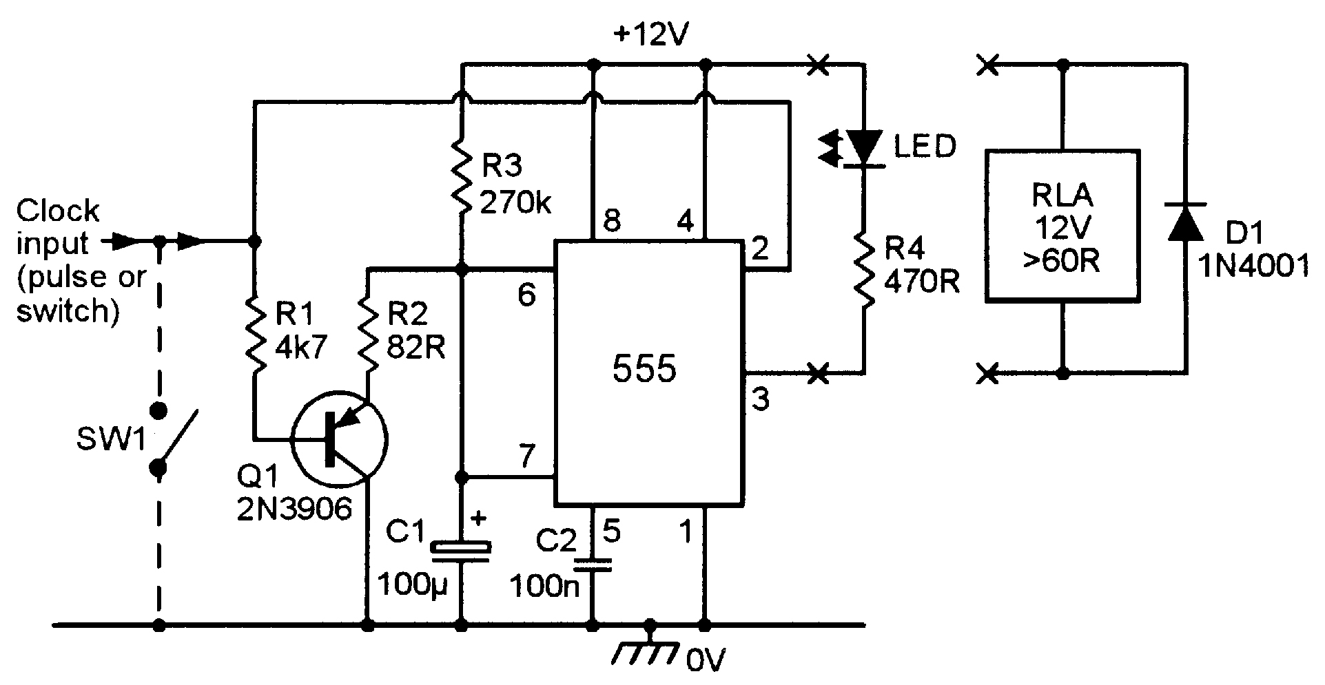
FIGURE 20. Event-failure alarm or missing-pulse detector with LED or relay output.
Thus, each time a clock pulse arrives, it rapidly discharges C1 via Q1 and simultaneously initiates a timing cycle that drives pin 3 high, but before the cycle can end, naturally a new clock pulse arrives and repeats this process. Consequently, pin 3 remains high so long as clocking input signals arrive within the prescribed period limit, but goes low and turns on the relay and LED if a clock pulse is missing or its period exceeds the pre-set limit. The circuit thus acts as an event-failure alarm or missing-pulse detector; with the component values shown, its natural monostable period is about 30s, but is variable via R3-C1 to suit individual needs.
Note in the Figure 20 circuit that the pin 2 trigger signals must be negative-going pulses with amplitudes that switch from an OFF value above 2/3 VCC (but not greater than Vcc) to an ON value below 1/3 VCC. NV
Next time, we'll show you ways of using the 555 IC in a variety of astable waveform generator circuits.