Customers sometimes require that our crystal controlled digitally synthesized 60 Hz oscillators be synchronized to the 60 Hz line. Synchronization is essential when you need to switch a load between two independent sources, such as the 60 Hz line and a 60 Hz oscillator (with a power amplifier). A simple relay can be used to switch between them. However, the sources must be synchronized. Otherwise, large potentially damaging transients will occur.
For example, suppose the oscillator and the line were the same voltage, but 180 degrees out of phase. The line would be at voltage +V, while the oscillator would be at –V. The load would see a transient voltage of 2V as the relay switches between sources. (For a line voltage of 115 Vrms, V can be anywhere from 0 to 160 volts, depending on when in the cycle the switching occurs. A 320 volt transient is possible). This stresses both the relay and the load, possibly to the point of doing damage.
If the 60 Hz line and oscillator output were synchronized and of the same magnitude, the switching would occur between two identical voltages with no transient at all. The conclusion is that if you want to switch a load between sources, they should be synchronized and of equal magnitude. This article shows how to achieve synchronization (identical frequency and phase) of the waveforms.
The oscillator frequency is determined by a quartz crystal, and the line frequency is controlled by the utility company. In some locations, this may vary by as much as ±0.5 Hz over the course of a day. The question is: How can we synchronize the crystal oscillator to the line? Almost by definition we cannot change the frequency of the crystal, yet it must be adjusted to the line frequency which may be anywhere from 59.5 Hz to 60.5 Hz.
It is possible to “pull” a crystal off of its nominal frequency by adding reactive components into the resonant circuit. This technique might be able to pull the crystal a few kHz off nominal.
Assuming the 15.36 MHz crystal can be pulled ±5 kHz, that represents about ±325 PPM (or ±0.02 Hz) which is not enough to cover a potential discrepancy of ±0.5 Hz.
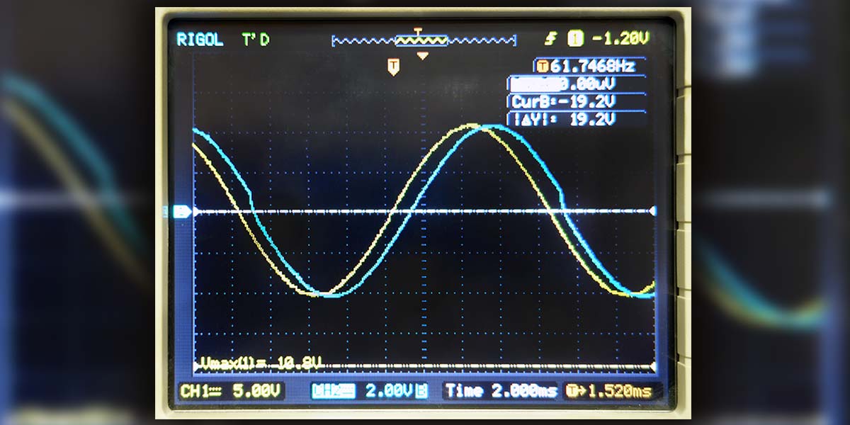
An effective technique used here is to distort the waveform so it fits in the allotted cycle time of the 60 Hz line. For example, consider the waveforms in Figure 1. The yellow trace is the (simulated) line signal running at 61.74 Hz, simulating a very high line frequency. The blue trace is the 60.00 Hz output of the crystal controlled oscillator, synchronized to the fast running line.
The synchronization circuit restarts the 60 Hz (blue) waveform at (nominally) the zero crossover of the 61.74 Hz waveform and effectively chops off a small segment of the oscillator’s 60 Hz waveform. This forces the 60 Hz oscillator waveform into the same time period as the 61.74 Hz line signal, at the expense of some distortion.
Figure 1 shows the restart of the 60 Hz (blue) waveform occurs at about 190 degrees of the (yellow) line waveform.
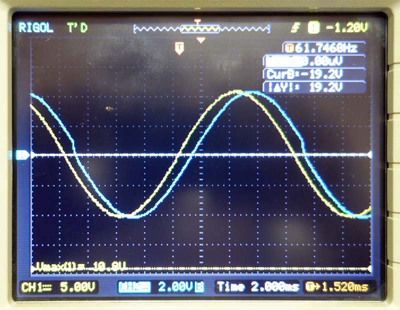
FIGURE 1. High line frequency. Line frequency (yellow) is 61.746 Hz. Oscillator frequency (blue) is 60.007 Hz. Oscillator frequency (blue) restarts at about 190 degrees of the (yellow) line waveform. A segment of the oscillator output has been chopped off to make the oscillator period equal to the period of the line.
Figure 2 shows a more normal situation where the line frequency is 59.79 Hz, the oscillator frequency is 60.007 Hz, and the difference is 0.217 Hz. There is no discernible distortion, and the signals are synchronized but slightly out of phase. The phase difference is allowed here to more clearly distinguish the waveforms, and will be corrected later.
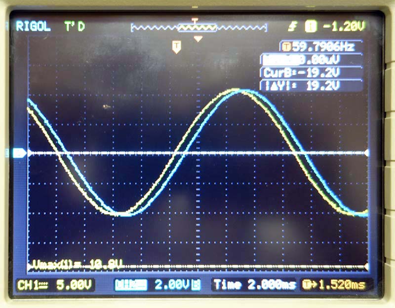
FIGURE 2. Normal line frequency. Line frequency (yellow) is 59.79 Hz. Oscillator frequency is 60.007 Hz. Difference is 0.217 Hz. Signals are synchronized with no discernible distortion.
Figure 3 shows a low line frequency of 57.835 Hz. The oscillator frequency is 60.007 Hz. The oscillator must run more than 360 degrees to fill the time period of the line. It also restarts at about 190 degrees.
FIGURE 3. Low line frequency. Line (yellow) is 57.835 Hz. Oscillator (blue) is 60.007 Hz. The oscillator runs for slightly more than a full cycle, thereby synchronizing to the slightly slower 57.835 Hz line.
These photos illustrate that synchronization using this method creates distortion that becomes negligible for small differences in frequency. Furthermore, the distortion occurs when the voltage is near zero volts, suggesting that the energy of the distortion is very small.
Most practical cases resemble Figure 2 where the distortion is essentially absent. The more extreme cases of Figures 1 and 3 are shown to aid understanding of this technique.
A synthesized function generator was used to simulate the line voltage for these photos. This allowed us to easily change the line frequency for our test purposes. The photos show how the oscillator is synchronized to any line frequency by fitting the oscillator signal into the period of the line, either by chopping off a slight bit of the waveform or letting it run for a little longer than one cycle to fill up the period of the line. This may cause some distortion of the oscillator waveform, but under normal conditions the distortion is negligible.
The small phase difference between the traces is partly due to the zero crossing detector (look ahead to Figure 6) which does not switch at precisely the zero crossing. However, the phase difference can be removed in software as will be described shortly.
Oscillator Operation
Before presenting the synchronizing software (in flowchart form), it is necessary to understand how this oscillator works. The synthesized oscillator uses NXP Semiconductors’ (formerly Freescale and before that Motorola) eight-bit MC9S08SE4 microcontroller.
This processor contains an index register called ‘h:x’ where h and x are independent eight-bit registers. (The semicolon between h and x indicates that these registers are concatenated. They are read as one 16-bit register, even though they are two independent eight-bit registers.) They are used to point to locations in memory that contain a sine wave lookup table.
In our case, h:x has been chosen to start at $f300 (‘$’ means a hex number) and end at $f3ff. The h register remains fixed at $f3, and the x register cycles through 00, 01, 02,…FE, FF, 00, 01, etc. Each memory location contains a point on the sine wave. There are 256 points (0-255), and each step is 360/256 = 1.40625 degrees. A table of memory locations is shown in Figure 4A.
| Memory Location |
Sine Wave Amplitude |
| $f300 |
Amplitude for N=0 |
| $f301 |
Amplitude for N=1 |
| $f302 |
Amplitude for N=2 |
| $f303…$f3fc |
N=3 to N=252 |
| $f3fd |
Amplitude for N=253 |
| $f3fe |
Amplitude for N=254 |
| $f3ff |
Amplitude for N=255 |
FIGURE 4A. Memory contents per memory location.
The amplitudes in the table are calculated from the equation:
Sine Wave Amplitude = 128 + 127sin(1.40625 x N) with 0<=N<=255
For example, for N=0, Amplitude = 128 (angle = 0 degrees)
N=64, Amplitude = 255 (angle = 90 degrees)
N=128, Amplitude = 128 (angle = 180 degrees)
N=192, Amplitude = 1 (angle = 270 degrees)
This represents a sinusoid with a zero line of 128, a positive peak of 255, and a negative peak of 1.
For purposes of this discussion on the basic operation of the oscillator, it is important mainly to understand that cycling through the x register points to a complete sine wave cycle. We are now ready to understand the oscillator as represented in the flow chart of Figure 4B.
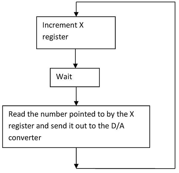
FIGURE 4B. Oscillator flow chart.
Assume for the moment that the Wait time is zero (no wait). The fastest possible sine wave (for this processor and this software) will occur. A point on the sine wave will be sent to the D/A (digital-to-analog) converter. The X register will be incremented to the next point in memory. It will be sent to the D/A converter and so on. The X register will race around from $00 to $FF repeatedly, thereby repeatedly describing complete cycles of sine waves at the output.
Now, suppose we introduce a Wait time of exactly 65.10416667 microseconds (how to get this exact delay will be told momentarily). Each new point on the sine wave will be sent to the D/A converter every 65.10416667 microseconds. Since there are 256 points on the sine wave, 256 points will take 256 x 65.10416667 = 0.0166667 seconds, which is the exact period of 60 Hz! In other words, this Wait time produces a sine wave with a frequency of exactly 60.000 Hz.
The Wait box in the flow chart creates the delay by waiting for an interrupt from the timer system of the processor. Using a 15.36 MHz crystal, this processor will generate a bus frequency of 15.36 MHz/2 = 7.68 MHz.
The timer system is thereby driven from a clock with a period of 1/7.68 MHz = 130.2083333 nanoseconds. The internal timer counter is programmed to be a modulo 500 counter so that it overflows and jumps back to 0 at a count of 500. Note that 500 x 130.2083333 ns = 65.10416667 µs.
The processor is programmed to interrupt at every overflow of the modulo 500 counter. The resulting interrupt service routine lets the processor pass the Wait state and go on to create a point on the sine wave every 65.19416667 µs.
If a modulo 600 counter were used instead of the modulo 500 counter, interrupts would occur at 600 x 130.2083333 ns = 78.125 µs, and the output period is 78.125 µs x 256 = 0.02 seconds, or 50 Hz exactly.
Using a modulo 75 counter produces exactly 400 Hz. Thus, the three main power frequencies can be precisely synthesized with a 15.36 MHz crystal, which is a stock part with many distributors.
It is important to recognize that for 60 Hz, the interrupts are spaced 65.18416667 µs apart. The time necessary for reading the table, sending the data out to the D/A converter, and incrementing the index register all take place during the time between interrupts and subtract from the time in the Wait state.
For example, suppose it takes a total of 30 µs to read the table, send the data out, and increment X. Then, 30 µs will already have passed and the system will stay in the Wait state for only another 65.18416667 – 30 = 35.18416667 µs until the next interrupt occurs. In other words, part of the interrupt time period is used to do necessary tasks and not just waiting.
This system produces exactly 60 Hz, subject only to the accuracy of the 15.36 MHz clock. It remains now to adjust this frequency to the line frequency, which may deviate from exactly 60 Hz.
Synchronizer Operation
The synchronizer adds some extra steps into the flow chart in Figure 5. Its function is to restart the waveform on the positive going zero crossing of the line voltage. This either chops off a small segment of the 60 Hz waveform or extends the running time of the 60 Hz waveform; in both cases, to make it have the exact period of the line.
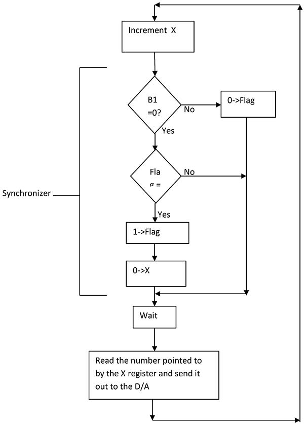
FIGURE 5. Flow chart of oscillator with synchronizer.
The line voltage cannot be connected directly to the microcontroller. It is connected through an optocoupler such as a 4N35. The circuit is shown in Figure 6.
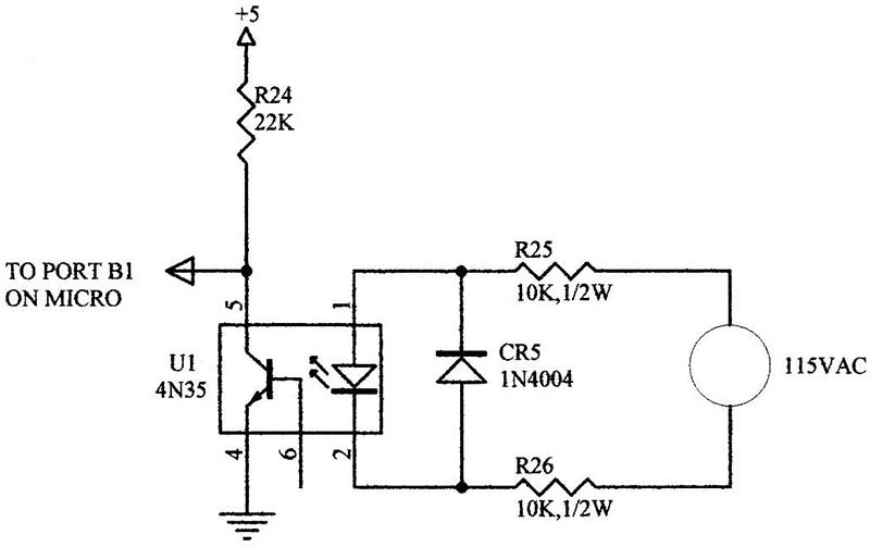
Line Isolator and Zero Crossing Detector
FIGURE 6. Optocoupler circuit.
Optocoupler U1 isolates the microcontroller from the AC line. R25 and R26 are selected to limit the power dissipation of each resistor to about 0.33 Watts. The 115V line must rise to about 10V to cause a transition at B1, which means that it detects about 4 degrees and not the zero degree crossover. The resulting phase discrepancy is corrected in software.
The optocoupler — in addition to isolating the line — creates an inverted square wave replica of the line at port B1 of the micro. When the line goes positive, the square wave is logical zero; when the line goes negative, the square wave is logical 1. A photo showing the simulated line voltage and the signal at the B1 port on the microcontroller is shown in Figure 7.
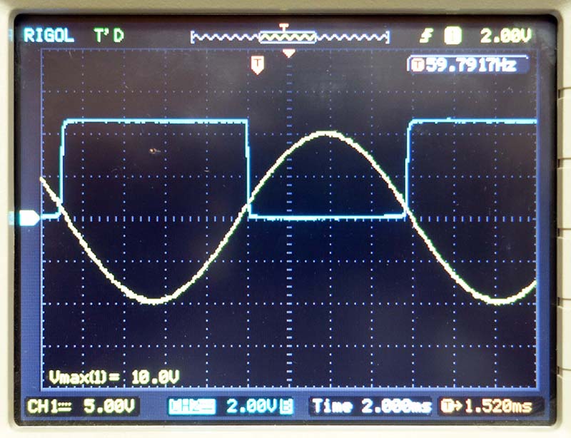
FIGURE 7. Optocoupler output (blue) vs. simulated line voltage (yellow).
Consider the case where no line voltage is applied. The signal at B1 will be continuously High. That is B1=1. The flow chart shows that under these circumstances, the main part of the synchronization logic will be bypassed, and only the flag will be repeatedly reset (with no effect). The oscillator will work just as previously described. In other words, the synchronization system has no effect if the synchronization signal (line voltage) is absent.
Consider next that the line voltage is connected. When the line voltage is negative, B1=1 and the system behaves as described above.
The instant that the line voltage crosses the zero axis in a positive direction, the signal at B1 goes from 1 to 0. When the oscillator reaches the decision point for B1, it will select ‘yes’ for B1=0 and proceed downward in the flow chart.
In the next step (Flag=0?), the answer will again be yes because the flag had been reset while B1 was high.
In the next steps, the flag will be set and the X register loaded with 0 (which is the start of the sine wave table in memory). This effectively restarts the oscillator at the top of memory and at zero degrees of angle.
The oscillator will proceed to load that memory value to the D/A converter, and then return to the top of the flow chart to increment X and again go through the synchronizer.
At that time, B1 will still be zero, so the process will proceed downward through the flow chart. Now when it reaches the decision point “Flag=0?,” the answer will be ‘no,’ the flow chart will bypass reloading the X register, and no further action will be taken. This shows how the X register is reloaded only once on the falling edge of B1 (equivalent to the positive slope zero crossing of the AC waveform). When the AC line eventually goes negative, B1 will return to 1 and the flag will be reset, thereby preparing for another cycle.
To summarize, the synchronizer reloads the X register with its zero phase setting on every falling edge of the square wave at B1, thereby forcing the waveform to restart in synchronism with the line.
Adjusting the Phase of the Synchronized Signal
Any phase relationship between the oscillator and line can be created by loading a memory location between 0 and 255 when the line crosses zero. The number selects at which point in memory and thereby what phase of the oscillator sinusoid shall coincide with the zero crossing of the line voltage. The photo in Figure 2 shows a small phase difference between the line and the oscillator. This can be corrected by loading a number other than 0 at the falling edge of B1. Loading 10 instead of 0 corrects the phase discrepancy. The signals are now synchronized exactly in phase and with no visible distortion as shown in Figure 8.
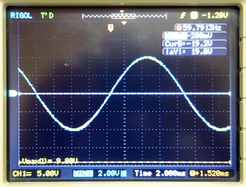
FIGURE 8. Signals are synchronized and in phase. Line (yellow) is at 59.79 Hz. Oscillator is at 60.007 Hz. Synchronizer uses 10 instead of 0 as the restarting memory location.
Hardware and Test Setup
Figure 9 shows the complete oscillator board. The microcontroller (MC9S08SE4) is the 28-pin DIP IC on the right side of the board. Further to the right is the six-pin optocoupler (4N35). I like using DIP packages wherever possible because they’re accessible to humans. The lead spacing is 0.1 inch which is fine for hand soldering.
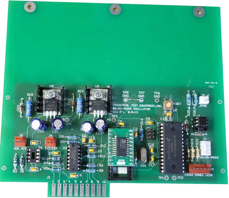
FIGURE 9. The ‘9S08-50/60/400’ oscillator board.
SMD packages start at 0.050 and go down to 0.01 lead spacing which is impossible to solder by hand. If there’s any doubt about an IC, the DIP sockets allow quick and easy replacement without damage to the board.
The TO-220 packages on the left side of the board are voltage regulators. On a new board, I first remove all ICs and check the ±5V supplies. This assures that the ICs will get correct power and I don’t wind up with a board full of dead chips due to power supply problems.
The six-pin programming header is located slightly to the left of the MC9S08SE4. It is used to program the micro. The SMD IC in the center of the board is a four-channel D/A converter. It uses an SMD to DIP adapter board because a DIP version of this IC was not available. (It is a four-channel D/A converter which is used for three-phase operation of this oscillator).
Figure 10 shows the oscillator installed in a unit. The oscillator is mounted on the side wall and has been trimmed down in size to fit this mounting requirement. The driver PCB (printed circuit board) is also mounted on the side wall (to the left of the oscillator).
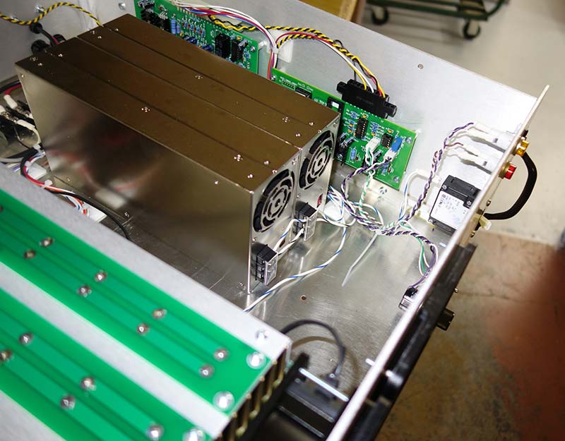
FIGURE 10. Oscillator as installed in a Model 500S-CRH (500W AC current source). The oscillator PCB has been trimmed to fit on the side wall of the unit.
Two switching power supplies are in the middle of the photo. They provide the DC power for the unit. The FET (field effect transistor) bank is in the left foreground. It provides the amplification of the oscillator signal.
Conclusion
Though the science of synchronizing one analog signal to other analog signal is somewhat well-trod ground, you can see how the introduction of digital systems has created new and surprisingly interesting challenges for synchronization.
I think it’s important to note that the approach used in this article is just one of many possible ways to solve this particular problem, and I hope you have enjoyed this in-depth look at how we tackled it. NV