In the first part of this series, you learned about the physical Controller Area Network (CAN) bus, bus arbitration, device addresses, and address masks and filters. Not all MCUs include a CAN controller and even those that do can challenge experienced designers. In either case, an external Microchip MCP2515 CAN controller IC can do the job, and you'll learn how to use it.
Because an MCP2515 operates outside an MCU, it can take less time to set up and use than some MCU’s built-in CAN controllers. The control registers, message buffers, and flags prove easy to understand, and C-code clarity improves. The MCP2515 18-pin DIP makes it simple to breadboard and test a circuit, or you can use an MCP2515 module, shield, or cape. Before you start to experiment with an MCP2515 IC, download and print its datasheet (pages 1 through 68) which provides complete register descriptions, diagrams, flow charts, and tables (see References).
An MCP2515 relies on Serial-Peripheral Interface (SPI) signals, so almost any MCU meets the interface requirements. The examples in this article use an mbed board with an NXP LPC1786 (ARM Cortex-M3) MCU that includes an SPI port. In addition to the three SPI signals (MOSI, MISO, and CLOCK), an MCP2515 needs a logic 0 chip select signal (/CS) along with power and ground. The internal bit rate clock requires an external crystal.
MCP2515 Architecture
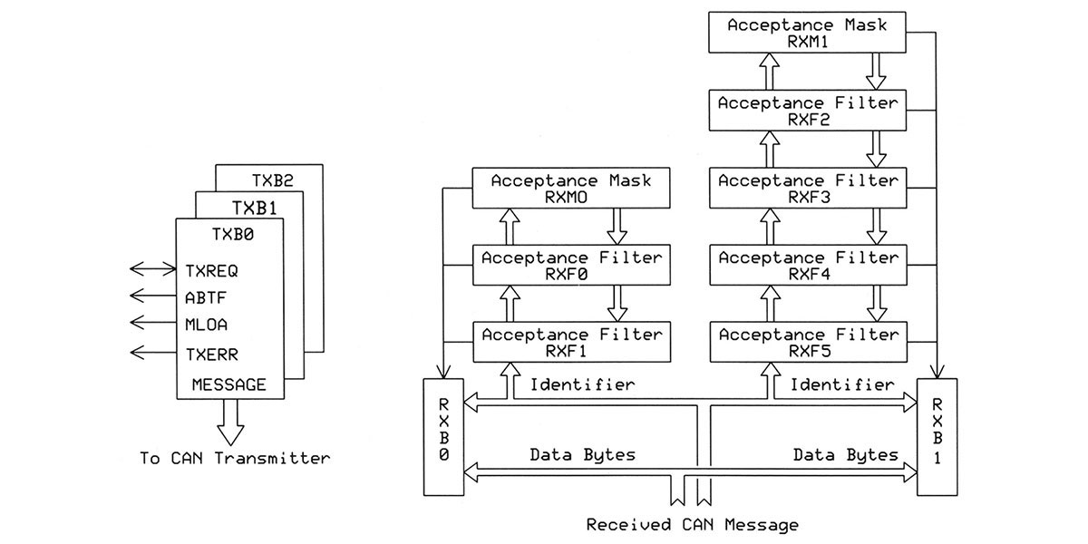
An MCP2515 CAN-controller IC comprises three transmitter buffers (TXB0, TXB1, and TXB2) and two receiver buffers (RXB0 and RXB1) which are shown in Figure 1.
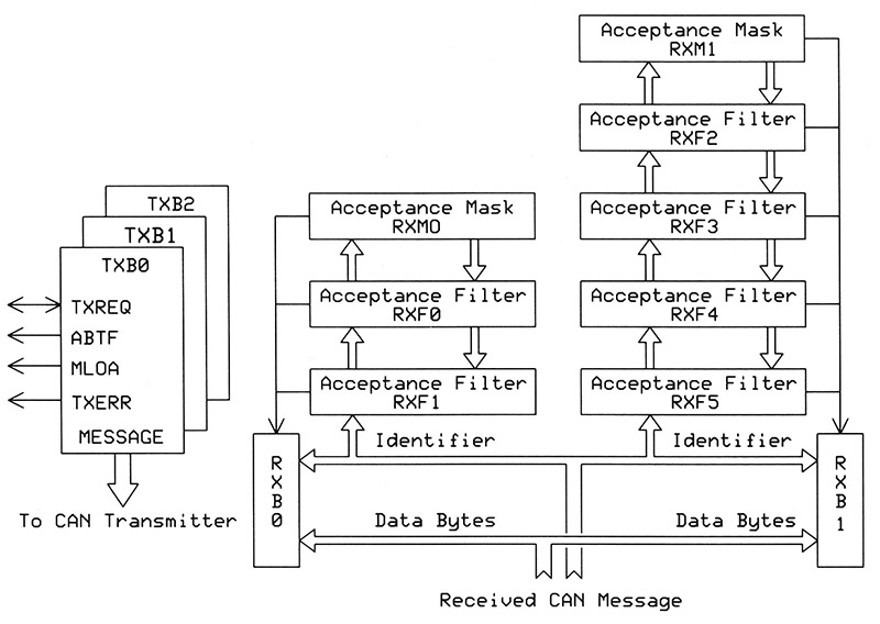
FIGURE 1. Each receiver buffer (RXB0 and RXB1) has its own set of masks and filters. Each transmitter buffer has registers for an 11- or 29-bit ID, a byte count, and as many as eight data bytes. For clarity, this diagram does not include all CAN-controller circuits. (The 29-bit address mode goes beyond the scope of this article.)
Receiver buffer 0 includes one acceptance mask (RXM0) and two acceptance filters (RXF0 and RXF1). Receiver buffer 1 includes one acceptance mask (RXM1) and four acceptance filters (RXF2 through RXF5). These masks and filters let you direct CAN messages to a specific buffer where the MCU can read it. You might use RXB0 for messages with a high priority address and RXB1 for other messages within an address range.
The three transmit buffers differ only by name. Each can hold as many as eight bytes of data, and each has associated control and status bits, as well as an interrupt. The receiver and transmitter buffers have the same organization (Figure 2) that comprises a control byte, two bytes for an 11-bit address, two bytes for an extended address (18 additional bits), a byte that stores the number of data bytes in a message, and those data bytes. (How can you put an 18-bit address in two bytes?
FIGURE 2. Register arrangement for receiver buffer RXB0 and transmitter buffer TXB0. Other buffers have the same register arrangement. Software may address these registers individually or sequentially.
The SIDL registers hold the two “extra” address bits, EID17 and EID16.)
In the MCP2515 datasheet, Table 11-1 shows what looks like a CANSTAT and a CANCTRL register for each buffer. Not so. An MCP2515 has only two registers that affect the CAN-controller and govern operating modes, provide buffer-interrupt signals, and set clock parameters. The datasheet calls all these bytes “registers,” so I’ll use that term from now on. An MCP2515 includes other registers that control flag bits and CAN bus bit rates.
Application software may identify a register by its address and then read from it or write to it. Register addresses run in sequence from 0x00 to 0x7F, but you needn’t try to memorize TXB0CTRL = 0x30, RXB1D0 = 0x76, and so on. Two C/C++ files — MCP2515JT.h and MCP2515JT.cpp — define register names and their addresses, which simplify programming and make code easier to understand.
An MCP2515 CAN-controller operates in one of five modes: Normal, Loopback, Configuration, Sleep, and Listen, as set by software. The Normal mode needs little explanation; it lets the IC operate as a device on a CAN bus (with a driver IC, of course). The Loopback mode “disconnects” the TXCAN and RXCAN signals from a bus driver and internally connects them. This mode lets people test the transmitter and receiver without disturbing other devices on a bus. This mode does not let you view the TXCAN signal with a scope or logic analyzer, however. (The Sleep and Listen modes go beyond this article’s scope.)
The Configuration mode provides the only way to change the communication bit rate, load the filter and mask registers, and preset several I/O pins. The MCP2515 enters this mode when it receives power, when it detects an external /RESET signal (logic 0), or when it receives a Reset command (0xC0). This command would come from an MCU via its SPI connection.
SPI Transfers Simplify Software
Although an MCP2515 contains 114 registers, the SPI port needs only nine commands to read and write data, modify a specific bit, cause a reset, and report status information. Table 1 summarizes the commands and their actions. Also refer to Table 12-1 in the MCP2515 datasheet.
All MCP2515 communications require only SPI write statements that take the form of spi.write(hex_value). The write operation in your MCU’s SPI library might have a different format. If so, open the MCP2515JT.cpp file and use search-and-replace operations to substitute your MCU’s SPI write instruction for spi.write.
Given the nine command types and hex values in Table 1,
| Instruction Name |
Instruction Description |
| RESET |
0xC0: Reset registers to default settings, enter Configuration mode. |
| READ |
0x03: Read a register’s content as a byte. |
| Read RX Buffer |
0x90: Read receiver buffer 0 ID.
0x92: Read receiver buffer 0 Data.
0x94: Read receiver buffer 1 ID.
0x96: Read receiver buffer 1 Data. |
| WRITE |
0x02: Write a byte to a register. |
| Load TX Buffer |
0x40: Load transmitter buffer 0 ID.
0x41: Load transmitter buffer 0 Data.
0x42: Load transmitter buffer 1 ID.
0x43: Load transmitter buffer 1 Data.
0x44: Load transmitter buffer 2 ID.
0x45: Load transmitter buffer 2 Data. |
| READ STATUS |
0xA0: Read the following bits as one byte:
D0: Receive-Buffer-0-Full Interrupt Flag
D1: Receive-Buffer-1-Full Interrupt Flag
D2: Buffer 0, Message-Transmit-Request bit
D3: Transmit Buffer-0-Empty Interrupt Flag bit
D4: Buffer 1, Message-Transmit-Request bit
D5: Transmit Buffer-1-Empty Interrupt Flag bit
D6: Buffer 2, Message-Transmit-Request bit
D7: Transmit Buffer-2-Empty Interrupt Flag bit |
| RX STATUS |
0xB0: Read bits to indicate a filter match and message type. |
| BIT MODIFY |
0x05: Set or clear individual bits in a register. (Does not apply to all registers.) |
| Request to send a message from transmit buffer |
0x81: Request to transmit message in buffer 0.
0x82: Request to transmit message in buffer 1.
0x84: Request to transmit message in buffer 2. |
TABLE 1. SPI Instruction Set for MCP2515
my MCU resets an MCP2515 with the command 0xC0 sent this way:
spi.write(0xC0);
You can use a command or register name to make code easier to understand. The file MCP2515JT.h contains all register definitions such as:
#define RESET_REG 0xC0
and this definition lets you write a code statement:
spi.write(RESET_REG);
The MCP2515JT.h file also provides prototypes for MCP2515 control functions such as: send_0, load_0, readDATA_0, and readRegister. SPI commands and operations will become clearer as you review a code example shown later.
Set Up an MCP2515 Circuit
I created a test circuit (Figure 3) that connects an MCP2515 to an mbed MCU board.
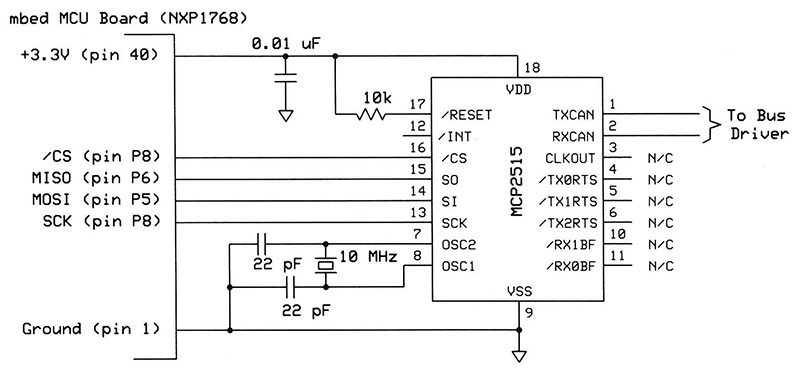
FIGURE 3. Schematic diagram for MCP2515 connections with an mbed NXP1786 MCU. My circuit used 3.3V power from the mbed board, but an MCP2515 will operate with a VDD between 2.7 and 5.5 volts. This circuit does not connect to a CAN bus driver IC.
SPI pin numbers depend on the MCU you’ll use, but SPI ports usually work the same way. The MCP2515 uses SPI mode 0,0 or 1,1 and transmits the most-significant bit (MSB) first for each byte, or register. My circuit used a 10 MHz crystal, although some commercial modules include an 8 or 16 MHz crystal. The crystal frequency and calculated timing values govern the CAN bus bit rate.
The MCP2515JT.cpp software includes places for three bit-timing values — CNF1, CNF2, and CNF3 — in the baudConfig function for standard CAN bit rates. You must calculate bit-timing values based on your crystal’s frequency and the bit rates you plan to use. Then, insert the calculated values in the MCP2515JT.cpp file to replace the 0x00 “placeholders.” I calculated values for 125,000 bits/sec and used them as shown in the following:
//Set CAN timing constants for 125,000 bits/sec
case 125:
//Jon’s values for 10.00 MHz XTAL
CNF1 = 0x01;
//Value for MCP2515 CNF1 register
CNF2 = 0xBA;
//Value for MCP2515 CNF2 register
CNF3 = 0x07;
//Value for MCP2515 CNF3 register
break;
I used 125 kbits/sec for tests, and didn’t need any other timing values. Always document code changes, timing values, and crystal frequency!
Two online calculators give you bit rate timing values for almost any crystal frequency (see References). I ran the Seeed Studio bit-timing software to calculate timing constants that worked well. You can download the Windows CAN timing software from the Seeed Studio website at http://wiki.seeed.cc/CAN-BUS_Shield_V1.2/#generate-a-new-baudrate. The GUI uses Chinese characters, but you’ll see labels in English for the important controls.
Transmit a CAN Message
Before you create an application program, ensure your MCU’s SPI port operates properly and ensure you have changed — if necessary — the spi.write statements to conform to the SPI functions for your MCU. I often write test programs within a simple LED flash loop that runs continuously. The flashing LED indicates code in the loop operates, although it might not do what I expect. I took this route for MCP2515 tests. You must have the MCP2515JT.cpp and MCP2515JT.h files in your “working” directory, along with any other files the MCU’s compiler needs; perhaps spi.h or stdio.h. The following steps describe operations used to configure an MCP2515, load a three-byte message, and send it:
- Define an array (data[8]) to contain data bytes. Preset the first three byte values as you wish.
- Reset the MCP2515.
- Put the MCP2515 in the Configuration mode.
- Set the baud rate at 125 kbits/sec with timing constants calculated for your MCP2515’s crystal frequency, and inserted by you in the MCP2515JT.cpp file.
- Return the MCP2515 to its Normal mode.
- Use the load_ff_0(3, 0x123, data) function to create a three-byte CAN message with the identifier 0x123 and to put it all in transmitter buffer 0. The three bytes come from the data array defined earlier. I find it easier to load all transmitter registers with one function rather than with a separate function for each register.
- Use the send_0() function to have transmitter buffer 0 send a CAN frame.
- Finally, a readStatus() operation lets me see activity — if any — on the MCP2515 serial-out (SO) pin. (I use a Saleae Logic brand logic analyzer to capture digital signals.)
Here’s the demonstration code that is also available below in the downloads. The download package includes the MCP2515JT.h and MCP2515JT.cpp files and three commented demonstrations:
//Program CANJT1.cpp See also file MCP2515JT.cpp
#include “mbed.h”
#include “MCP2515JT.h”
DigitalOut myled(LED1);
//define an LED output
char XXX;
//a do-nothing variable
byte data[8] = {0x00, 0x99, 0xF9};
//Array data, 3 bytes
int main()
{
reset(); //Reset MCP2515
setMode(CONFIGURATION);
//Put MCP2515 into CONFIGURATION mode
baudConfig(125);
//Set CAN-bus bit rate to 125
//kbits/sec
setMode(NORMAL);
//Back to Normal mode
while(1)
//While loop runs forever
{
myled = 1;
//LED-blink to show program runs
wait(0.1);
myled = 0;
wait(0.1);
//Load 3 bytes of data into Transmit buffer 0,
//load address 0x123, & point to data[x] array.
load_ff_0(3, 0x123, data);
send_0();
//Transmit the buffer-0 info via CAN-TX
//pin
XXX = readStatus();
//Read the status bits.
}
//End of while loop
} //end of main
Figure 4 shows the TXCAN output signal to which the CAN controller appended a cyclic-redundancy-check (CRC) value 0x0F0F. When expanded, the small “bubble” at the right end of the trace shows a “NAK,” or no-acknowledgment bit.
I had no other CAN device on the bus, so my MCP2515 did not receive an acknowledgment response, which it expected. Even so, the diagram shows the buffer transmission.
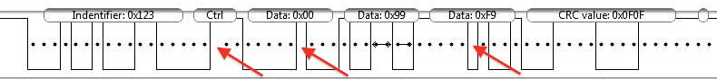
FIGURE 4. A trace of the TXCAN signal for the simple program shown earlier. My logic analyzer's CAN decoder option makes it easy to see the data as hex values. Three arrows mark "stuff" bits all CAN controllers introduce under special circumstances to synchronize timing between CAN devices.
Read a CAN Message
You might think a jumper between the TXCAN and RXCAN pins would let communications occur from the MCP2515 transmitter to the receiver. Not so. We have no bus and thus no other “transmitters” that would generate an acknowledgment bit. Thus, the MCP2515 receiver detects no proper acknowledgment and rejects the entire CAN frame, so we cannot use a jumper to test the CAN receiver. Instead, we put the MCP2515 in the Loopback mode. As mentioned earlier, the internal loopback connection does not affect any external circuits.
In Loopback mode, a receiver buffer should hold information sent from a transmitter buffer. Then, we can examine the receiver buffer and view the 11-bit ID, the byte count, and the data bytes sent by a test program. Before we can look at the register contents, our software needs two new statements that modify control-register bits but leave other bits unchanged.
So, how do we do that? The function bitModify in the MCP2515JT.cpp file does the job. It has the following format and requires byte sized arguments:
bitModify(register, mask, data);
During test runs, I wanted receiver buffer 0 to accept all messages, regardless of their 11-bit ID. The RXB0CTRL register includes two bits — RXM1 (D6) and RXM0 (D5) — that govern the acceptance masks and filters for that buffer. To disable the filters and masks, I must set only these two bits to 1. The other six control bits must remain unchanged. In this case, I used mask byte 011000002 to identify the two bits to change, and the data byte 011000002 to represent what I wanted those two bits to change to:
bitModify(RXB0CTRL, 0x60, 0x60);
Figure 5 shows the RXB0CTRL register contents before my program used the bitModify function.
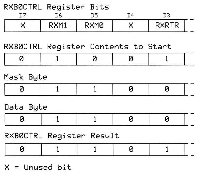
FIGURE 5. This example shows how the bitModify function changes the state of only the RXM1 and RXM0 bits in the RXB0CTRL register. The mask byte must hold a logic 1 for any bit position(s) you want to change. The data byte controls the final state of those selected bits.
The mask byte indicates which bits the data byte may change, and the data byte of 011000002 causes the RXM1 and RXM0 bits to contain 1s. Caution: Don’t confuse bit-wise masks used with bitModify operations with the acceptance masks used to set ID-filter characteristics (see Figure 1).
I need one more bitModify function in the test program. When a buffer receives a valid frame, it “notifies” the MCU via a flag bit in the CANINTF (CAN interrupt flag) register. A 1 indicates “data ready,” and a 0 indicates “no new data.” Software can read this register regularly and test the RX0IF (D0) bit associated with receiver-buffer 0 or the RX1IF (D1) bit for receiver-buffer 1.
When a flag bit indicates new data has arrived, software can read it and clear the RXnIF bit. According to the MCP2515 datasheet:
“This bit [RX0IF or RX1IF] must be cleared by the MCU in order to allow a new message to be received into the buffer. This bit provides a positive lockout to ensure that the MCU has finished with the message before the MCP2515 attempts to load a new message into the receive buffer.”
So, our test program must clear the RX0IF and RX1IF bits to logic 0s before we transmit a new frame to one of the receivers. Another bitModify statement handles this task:
bitModify(MCP2515INTF, 0x03, 0x00);
I added two new functions — readSID0_asHex() and readSID1_asHex() — to read receiver-buffer standard 11-bit addresses and convert them to a single hexadecimal value. The CANJT2.cpp program in the download package illustrates the address-read and address-display code.
SPI Register Access
The CANJT2.cpp program reads the RXB0SIDH and RXB0SIDL registers and displays the equivalent hex ID in a terminal window. I used the Parallax Serial Terminal (PST) and TeraTerm software at 9600 bits/sec (8N1) to receive data from the mbed MCU board via a virtual serial USB port. The terminal window should display “RXB0 ID = 0AA” and “RXB1 ID = xxx” again and again, where a hex address replace the xs. The RXB0 ID equals “0AA” because it’s the address set in the code. You may change the address and run the program again to ensure the receiver got a message with the new address.
Figure 6 shows a portion of the SPI signals sent to and from the MCP2515 CAN controller when I ran the CANJT2.cpp program. The upper trace shows MOSI activity; that is, data sent to the MCP2515.
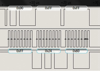
FIGURE 6. The top trace shows the MCU transmitted 0x90 to the MCP2515, which causes the CAN controller to point to the RX0SIDH register.
The middle trace shows the SPI clock, and the bottom trace shows the SPI data sent from the MCP2515 to the MCU.
The test program calls the function readSID0_asHex in the MCP2515JT.cpp file. This function includes the statement spi.write(READ_RX_BUF_0_ID); which sends 0x90 to the MCP2515 (see Table 1). However, this statement does not transfer any information to the MCU. You can see the 0x90 instruction in the upper trace and eight clock pulses below it. The 0x90 “tells” the CAN controller to point to the RXB0SIDH register.
The next two statements in the readSID0_asHex function each transmit 0xFF to the MCP2515:
HiAddr = (unsigned short) spi.write(0xFF);
LoAddr = (unsigned short) spi.write(0xFF);
Only the MCU acts as the SPI master and only it can generate SPI clock pulses. Thus, the MCP2515 communicates information to the MCU only when the MCU creates the needed clock signals. In this example, the 0xFFs amount to “do nothing” instructions the MCP2515 ignores. However, the two sets of eight clock pulses from the MCU cause the MCP2515 to send the RXB0SIDH and RXB0SIDL bytes into the MCU. HiAddr stores the RXB0SIDH (0x24) value and LoAddr stores the RXB0SIDL (0x60) value.
The function finally manipulates the bits and returns a hex value to the calling program. Remember, the SIDH and SIDL registers save bits in an “offset” manner. Addresses in filter and mask registers use the same bit formats.
Update Your Address
You might ask, “Okay, the MCP2515 pointed to the SIDH register, so how does it get data from the SIDL register, too? There’s no command to point to that register.” After the MCU points to a register and performs a read or write operation, the CAN-controller automatically increments the address to point to the next sequential register. If you must read bytes from, say, all the RXB0 registers, you don’t need to address each individually. Just start with the SIDH register and continue to send 0xFF do-nothing instructions. Each time you do, the MCP2515 will continue to send the MCU all the register bytes in order: RXB0SIDH, ...SIDL, ...EID8, ...EID0, ...DCL, ...D0, and so on. You could create a loop to read all 13 registers and save their values in an array for later use. In the MCP2515JT.cpp file, you will see several such loops. After you retrieve data bytes, use them as you wish.
The MCP2515JT.cpp file includes the functions setMask_0 and setMask_1 that set the receiver masks (RXM0 and RXM1). It also includes six new functions (setFilter_0 through setFilter_5) that let you put values in mask or filter registers. These functions take a hex value between 0x000 and 0x3FF (0 to 2047).
You can experiment with these registers to see how they affect receipt of data with different addresses from the transmitter. Note: Software can change filter or mask information only when you put the MCP2515 in its Configuration mode. For an example that demonstrates CAN-filter operation, see CANJT3.cpp and try it. The listing includes instructions.
Coming Up
In the final article about the MCP2515, you’ll learn about lags and interrupts, how to interpret bits on the CAN bus, and why other CAN devices must acknowledge receipt of messages. NV
References
Microchip MCP2515 datasheet, DS21801G:
ww1.microchip.com/downloads/en/DeviceDoc/21801e.pdf
For Serial Peripheral Interface (SPI) information, visit:
https://en.wikipedia.org/wiki/Serial_Peripheral_Interface_Bus
For CAN timing calculations, visit:
http://wiki.seeed.cc/CAN-BUS_Shield_V1.2/
For an online CAN timing calculator, visit:
www.intrepidcs.com/products/free-tools/mb-time-calculator/
Yoshito Onishi, Kyle Crockett, and Patrick Cruce created the original MCP2515 code, which I used and modified. Thanks, guys, I appreciate your work.
Downloads
What’s in the zip?
Source code