Over the years, I have accumulated a bunch of chips from before the era of true PCs (Photo 1) when computers with names like Altair, KIM-1, and Cosmac ELF were popular. I’ve been looking for a way to use them in new projects, but until now I’ve held back for a couple of reasons.
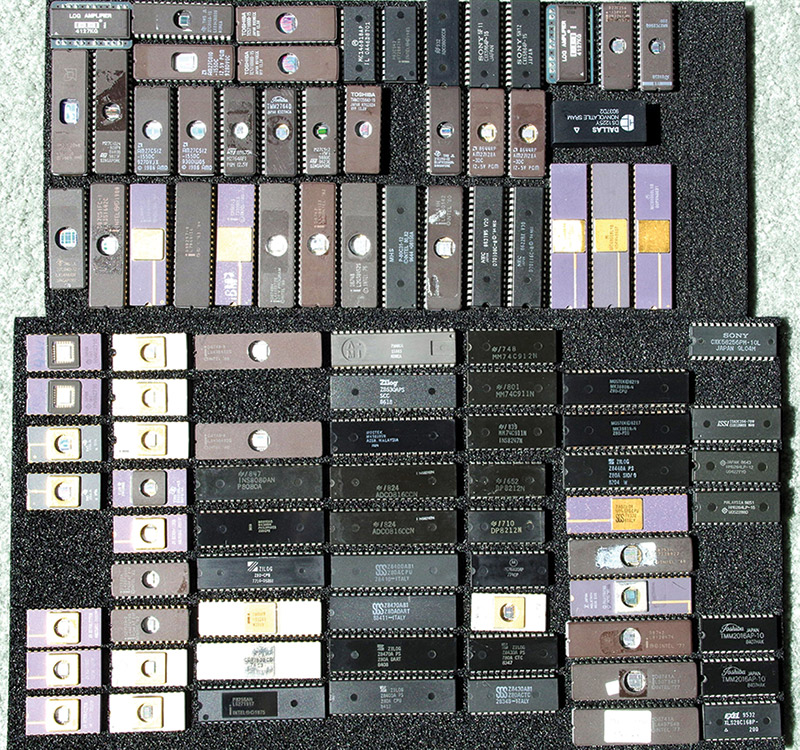
PHOTO 1. CPUs, RAMs, EPROMs, and support chips — all waiting to be reused.
First, I’m not a very good programmer and I don’t do assembly language; and second, those computers stored their code in EPROMs (programmable read-only memory chips that were erased with ultraviolet light through a clear window in their cases) and I didn’t have an EPROM programmer. After looking at some of the proposed schematics for Z80 based systems at www.z80.info, I was inspired to design such a system (Photo 2) around a 40-pin PIC16F887 which I do know how to program. I figured this would put some of my historic chips to work and be a great learning tool for understanding how a microcomputer works.
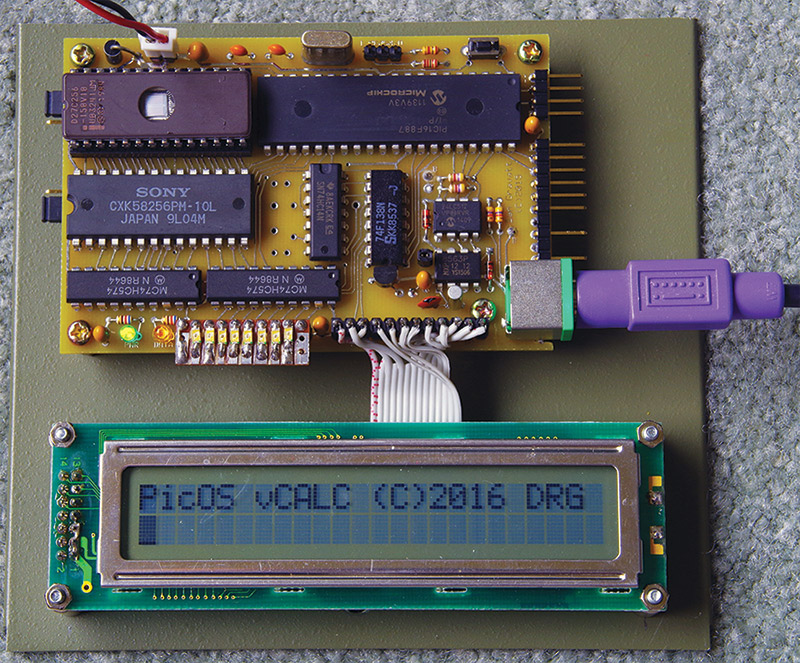
PHOTO 2. The PIC SBC.
In general, a microcomputer is a small (relative to a mainframe — the other type of computer in use when this term was coined in the 1970s) self-contained computer with separate CPU, RAM, ROM, I/O, and some sort of non-volatile storage medium, with the separate components linked by address and data buses that can be expanded to include additional devices. A microcontroller, on the other hand, has these separate components merged on a single chip with limited amounts of memory and I/O, and usually no expansion buses. I’ve used microcontrollers for years and love their simplicity, but when programming them with high-level languages it’s easy to forget what’s going on “under the hood” between those various components. Sometimes a better knowledge of the hardware-level processes can make you a better programmer and debugger.
For this project, the PIC gets treated like a true CPU with PortC as a dedicated address bus and PortD as a dedicated data bus (Figures 1a and 1b).
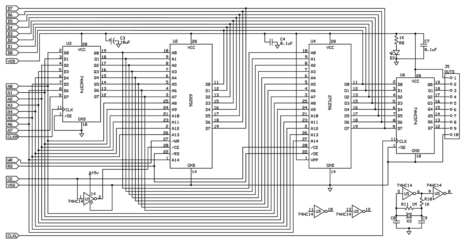
FIGURE 1A. Schematic of the CPU and I/O portions of the SBC.

FIGURE 1B. Schematic of the memory and latch portions of the SBC.
The PortC address bus connects to static RAM and EPROM totaling 64 kilobytes, and uses an eight-bit latch to form the necessary 16 address lines. The PortD data bus connects to the RAM and EPROM, as well as an eight-bit output latch and an alphanumeric LCD. Size constraints on the circuit board kept me from including more period-appropriate peripheral chips such as the 8255 parallel I/O controller, the MC146818 real time clock (RTC), and some sort of disk controller chip, so I had to compromise the “retro” nature of the project a bit by including an I2C bus for the RTC and nonvolatile storage EEPROM.
Of course, a computer needs a keyboard and a display, so there’s a PS/2 keyboard interface and an RS-232 serial link to use an old laptop computer as a “dumb terminal.” The block diagram in Figure 2 shows the functional relations between all these parts. Let’s dive in and see how to make these parts work together.
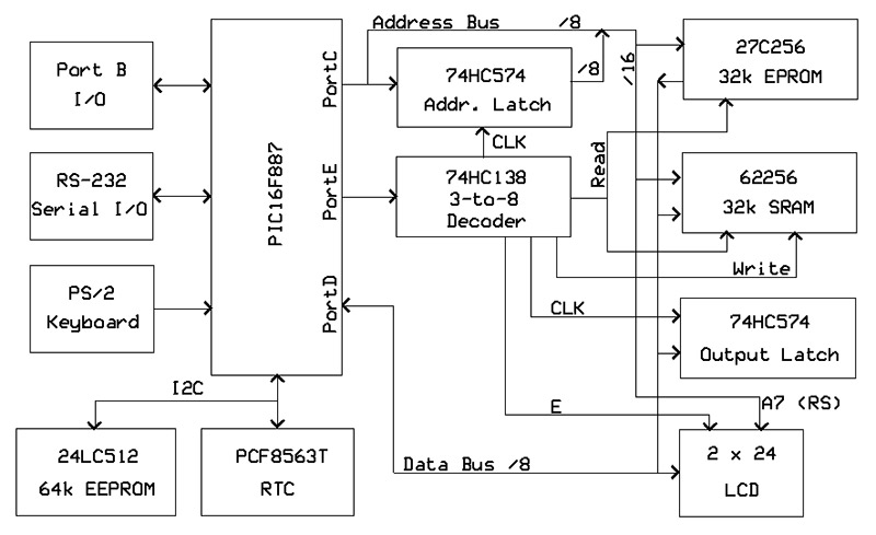
FIGURE 2. Block diagram of the SBC.
Keyboard
The PS/2 keyboard uses a synchronous serial interface to send 11-bit packets of data to the host computer, with the keyboard generating the clock signal for the interface (see References). PS/2 keyboard scan codes are a random nightmare — there’s just no other way to describe them. Take a look at the spreadsheet I created (available at the article link) to help me figure out how to translate them into ASCII. The keyboard sends data both when you press a key (usually one or two packets) and when you release it (usually two or three packets), but most of that data is irrelevant for our purposes.
If that wasn’t complicated enough, paired keys like shift, ctrl, alt, numbers, and enter send different codes depending on which one you press! There is no formula that can transform the scan code data into the corresponding ASCII character, so I used the 256-byte EEPROM in the PIC as a one-to-one translation matrix, where the scan code is the address of the byte containing the character.
The code for keyboard input supports the core functions (all characters, shift, backspace, enter, escape) necessary for this project without taking up too much code space, and without using interrupts. It works well with a 4 MHz clock speed as long as you are not a super-fast typist. See the comments in the code at the article link for more on how it works.
Memory
CPU communication with external memory consists of an address bus to select the required byte, a data bus to either read or write that byte, a chip select signal to activate only the desired chip on the bus, and read and write signals to tell the memory chip whether to send or receive data. The CPU starts by placing the address on the memory chip’s address inputs, and then places data on the data bus (for a write) or sets its data bus pins to inputs to read data. The desired memory chip is activated with its individual chip select input, and then its read or write input is activated to complete the transfer.
The order and timing of these steps is specified in the datasheet for each type of memory chip (see References). This project uses a 62256 32 kilobyte static RAM and a 27C256 32 kilobyte EPROM. The EPROM can be hard to find as a new part, so use one from your collection of vintage chips. Address bit A15 is used to handle the chip select signal for the two memory devices through an inverter logic gate, so one or the other chip is always selected. Address bits A0-A14 then select the byte within the selected chip. This means that sending the 16-bit address handles the chip select and byte address simultaneously, which is okay if you respect the overall signal timings for the chip.
The read and write signals are generated with the PIC’s PortE: a three-bit port that drives a 74HC138 three-to-eight decoder chip. Until the memory chip receives a read or write signal, its data bus connections are internally disconnected or “tri-stated” so they do not interfere with data transfers with other chips on the bus. When the signal is received, the selected memory chip accepts the data on the bus for a write, or places the data from the selected address on the bus for a read. I’ve placed a “Data” LED on output 0 of the decoder which will flicker when data is being transferred; it can also be used to send blink codes to the user.
From the PIC’s perspective, the PortC address bus and the PortE decoder bus are always outputs, but the PortD data bus must rapidly switch between outputs and inputs as necessary throughout the code. Look for lots of trisd = 255 and trisd = 0 statements in the code in the data transfer subroutines. Also look for the address latch operation that presents the 16-bit address to the bus as two separate bytes — similar to the way the old CDP1802 microprocessor and some others addressed their memory.
Latch and LCD
A true CPU can only use its data bus pins to drive the inputs of other logic chips because they are a “logic level” interface that has almost no capacity to supply current. They cannot directly control an LED, serial port, or any other device in the “real world.” In addition, since the data bus is usually busy talking to the memory, it cannot afford to be tied up with those functions. A variety of interface chips usually share the data bus to provide the necessary real world connections and free up the bus. Interface chips have their own read, write, and enable inputs, and are generally accessed similarly to memory chips except that they usually don’t use the address bus.
In this design, a 74HC574 octal latch acts as a simple output-only interface chip on the data bus. To use it, the PIC places a byte on the data bus and uses the 74HC138 decoder to send a pulse to the latch’s clock pulse input. The data is then available on the latch’s outputs and is no longer just “data,” but can be used to control real world devices.
The alphanumeric LCD in the project also acts a lot like a latch on the data bus. The HD44780 compatible display controller has an eight-bit data interface, a read/write input, an “RS” input which tells the controller whether the data on the bus is text to be displayed or a command to be executed (such as clearing the display), and an “E” input that latches the data into the controller. The RS input can be shared with address line A7 to save a pin on the PIC since you will never being accessing the memory at the same time you are writing to the LCD. The 74HC138 decoder’s active-low output drives the LCD’s active-high E latch input through an inverter. The high-level LCD control commands available in various PIC programming languages simply automate the process of presenting data bytes to the display controller and toggling the RS and E inputs to complete the data transfer. For this project, the R/W input of the controller is hard-wired to ground (write-only) on the LCD module itself.
I2C
The I2C bus is a true bus like the CPU’s address and data buses, in that multiple devices share the same connections to the CPU but can be accessed individually. In contrast to the separate parallel address and data buses discussed above, I2C provides data, address, chip select, and read/write control to its devices over a single synchronous serial connection. This greatly cuts down on the physical connections needed for the bus. Note that much of the schematic in Figure 1a is taken up by the wires for the CPU’s address and data buses. The tradeoff is that the I2C’s serial data streams transfer data more slowly than the parallel-mode buses.
For this project, we’re moving relatively modest amounts of data on the I2C bus a few bytes at a time to and from the PCF8563 real time clock chip, and up to 64K bytes for the 24LC512 EEPROM. The entire EEPROM contents can be read in a few seconds — not unlike the performance of an early eight inch floppy drive. Much of the time required for a write to the EEPROM is taken up by pauses to let the chip complete its write cycle, which is on the order of 5-10 milliseconds — an eternity in CPU time. This is an example of how better understanding the hardware improves your code. If you don’t allow for these pauses between write cycles, the writes will fail!
The EEPROM is internally broken up into 128-byte “pages” and supports a block-write mode where a single I2CWRITE instruction can save up to 128 bytes. This mode is faster than writing a byte at a time since there is only one 5-10 ms pause required per block. It also saves wear and tear on the EEPROM, which is guaranteed for a large but not infinite number of write cycles.
If you use this mode, you must keep track of the EEPROM addresses you are writing to so that the block write does not cross a page boundary and garble your data in the process. This does not affect read operations from the EEPROM, which can start and end anywhere.
The PCF8563 RTC can be hard to find in an eight-pin DIP package. I’ve specified a surface-mount part in the Parts List because it is readily available. You can use a commercially-available adapter to attach the SO-8 package to the circuit board, or fabricate a “spider” adapter from some leftover resistor leads. The DS1307 RTC is available in a DIP package and is mostly pin-compatible with the PCF8563, so you could substitute that with some modifications to the code and circuit board.
Stack
CPUs and microcontrollers have a small array of registers that are used to store the address of a program instruction that jumps to another instruction location but needs to be able to find its way back to where it started, such as CALL or GOSUB. This array is called a stack, and it is limited in size. The PIC16F887 has an eight-level stack that can support eight nested CALLs (i.e., a CALL within a CALL within ...). PICBasic PRO uses four of these levels for its own internal purposes, leaving four nested levels for use in your code.
I learned the hard way that neither the PIC nor PICBasic PRO will warn you if you write code that creates a stack overflow by trying to store too many addresses on the stack. You can’t read the stack pointer to tell how many levels have been used, so you have to keep track manually while coding. Reading the fine print of the PIC’s datasheet may be overwhelming, but it will help your coding and debugging!
Putting It All Together
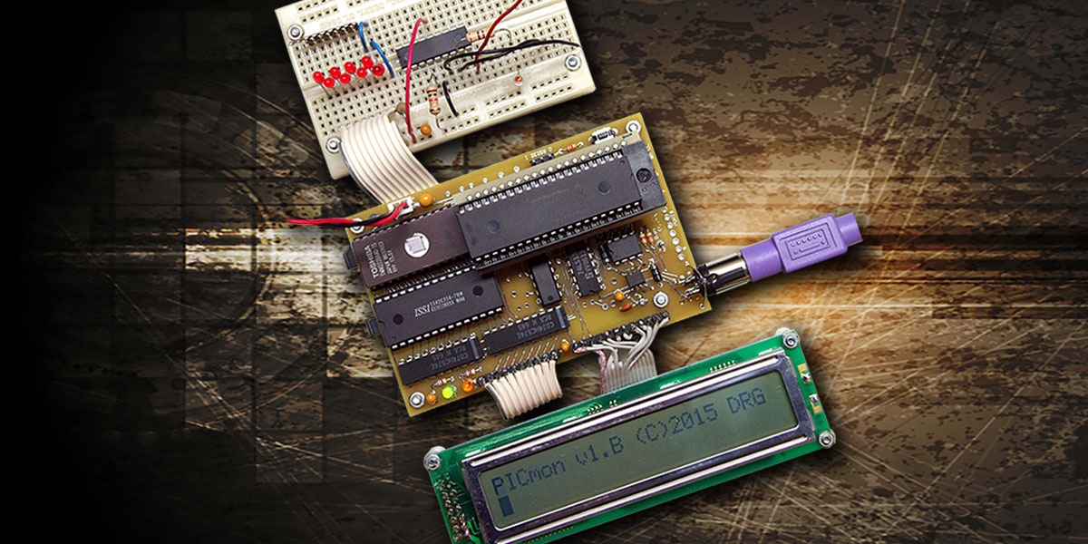
While it is theoretically possible to breadboard this circuit (Photo 3), you’ll really want a circuit board.
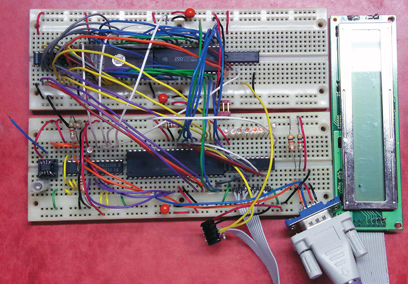
PHOTO 3. Prototype SBC on breadboards.
I’ve built some flexibility into the hardware — particularly with respect to the memory. The pinouts of the 62256 SRAM and 27C256 EPROM are not identical, but only the functions of pins 1 and 27 differ. I added two two-position jumpers on the back of the circuit board (not shown on the schematic for clarity) to swap the functions of these two pins (Write/Vpp and A14) and allow Socket 0 to hold a SRAM or an EPROM. If you have smaller capacity memory chips such as a 6264 8K SRAM or a 27C128 16K EPROM, these can also be used with some caveats. You’d think that the un-needed address pins for these chips would simply be “no-connect,” but sometimes they are used as additional chip select inputs. Check your datasheets carefully and either modify your code to set these inputs as necessary or break a trace or two on the circuit board to set them in hardware.
The schematic and PCB layout support a few other hardware options, including a general-purpose crystal oscillator using a couple of leftover inverters; an external crystal oscillator for the PIC for greater clock accuracy or if you want to run faster than its 8 MHz internal clock limit; access to the clock and interrupt outputs of the RTC chip; and a three-terminal analog temperature sensor. There is also an unused output on the 74HC138 decoder that can be used to access other data bus devices or drive a piezo speaker.
Note that there are no pads for R11 on the circuit board as I just couldn’t find space for it, so you’ll have to solder it across the pins of crystal X3 on the back of the board; the same goes for R12, the pull-up resistor for the open-collector CLKOUT pin of the RTC.
The circuit board holes for the case mounting tabs of J7, the mini-DIN PS/2 keyboard jack are not full size as they are too close to the edge of the board. Use a cutoff wheel or hobby saw to cut notches in the edge of the board to accommodate these tabs.
A potential application for this project is an EPROM programmer or “burner.” One of the Socket 0 jumpers isolates the programming voltage pin on the EPROM which is set at logic high for read operations, but typically needs around 13 volts for programming. A simple external circuit under PIC control (Figure 3) applies the programming voltage to the EPROM as needed and turns the project into an EPROM burner.
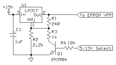
FIGURE 3. Voltage selector circuit for EPROM programming.
Check the programming voltage specifications for your particular EPROM and adjust the values of R2 and R3 accordingly. Make sure to UV-erase your EPROMs first; this sets all the bits to “1” and the burning process turns some of them into zeros. A better programmer than I could write a bootloader that would run PIC code stored on the EPROM to expand the 8K code space in the 16F887. The main reason that this project uses an eight-bit-at-a-time memory address scheme is to free up the eight PortB pins on the PIC for general-purpose I/O. Use them as another data bus to talk to some of your vintage interface chips on a separate circuit board, or take advantage of some of the special functions available on PortB like analog inputs or external interrupts.
The code I’ve written for this project uses a very simple command-line structure to select subroutines that demonstrate the hardware functions described above. Among other things, it will check for the presence of SRAM or EPROM in Socket 0 and adjust the SRAM start address accordingly. I’ve also included a very bare-bones file system to use the EEPROM as a tiny disk drive; its structure is explained in a separate tab of the reference spreadsheet available online.
A 9600 baud serial link with a laptop running a terminal program displays the list of files on the “disk” and supports data import to and export from the SBC. A command reference that explains how each subroutine works is also available online. There are plenty of comments to explain the code and help you roll your own PIC based operating system. So, dust off those vintage chips, read their datasheets, and build a microcomputer to call your own! NV
PARTS LIST
| ITEM |
PART # (DIGI-KEY) |
DESCRIPTION |
| U1 |
PIC16F887-I/P-ND |
PIC microcontroller, 40-DIP |
| U2 |
1450-1182-5-ND |
32 Kb static RAM, 28-DIP |
| U3, U6 |
(2) 296-1598-5-ND |
74HC574 octal latch, 20-DIP |
| U4 |
32 Kb EPROM, 28-DIP (see text) |
|
| U5 |
296-1577-5-ND |
74HC14 hex inverter, 14-DIP |
| U7 |
296-1575-5-ND |
74HC138 decoder, 16-DIP |
| U8 |
24LC512-I/P-ND |
64 Kb EEPROM, 8-DIP |
| U9 |
568-6650-1-ND |
PCF8563 real time clock, SOIC-8 |
| U10 |
LM34DZ/NOPB-ND |
LM34 temperature sensor, TO-92 (optional) |
| LCD |
NHD-0224BZ-FL-GBW-ND |
2x24 character display |
| D1, D2 |
1N4148FSTR-ND |
Signal diode |
| D3 |
754-1720-ND |
Green LED, T-1 |
| D4 |
516-1769-ND |
Amber LED, T-1 |
| D5 |
1N5399-E3/54GICT-ND |
Reverse protection diode |
| C1, C2 |
Optional, see PIC datasheet |
|
| C3 |
399-1418-ND |
10 µF tantalum |
| C4-C7 |
399-4151-ND |
0.1 µF ceramic |
| C8, C9 |
Optional, see text |
|
| C10 |
Frequency trim cap; see PCF8563 datasheet |
|
| R1 |
10KEBK-ND |
10K 1/6 watt |
| R2, R3, R6, R7, R12 |
4.7KEBK-ND |
4.7K 1/6 watt |
| R4, R8, R9, R10 |
1.0KEBK-ND |
1K 1/6 watt |
| R5 |
22KEBK-ND |
22K 1/6 watt |
| R11 |
1.0MEBK-ND |
1M 1/6 watt (optional) |
| SP1 |
445-2525-1-ND |
Piezoelectric beeper |
| X1 |
631-1081-ND |
4 MHz crystal |
| X2 |
300-3007-ND |
32 kHz crystal |
| X3 |
Optional, see text |
|
| J1-J6 |
S1011EC-40-ND |
0.1” straight header |
| J7 |
CP-1560-ND |
PS/2 Mini-DIN-6 |
| S1 |
ED3048-5-ND |
40-pin DIP socket |
| S2, S4 |
(2) ED3052-5-ND |
28-pin DIP socket |
| SW1 |
450-1665-ND |
SPST momentary switch |
| BT1 |
BS-7-ND |
Battery holder for CR2032 |
| (none) |
S1111EC-40-ND |
0.1” right-angle header for memory jumpers |
REFERENCES
“Legacy Communication with the 32-bit Micro Experimenter,” Nuts & Volts, October 2011
Retro microcomputer designs using the Z80
www.z80.info
Retro microcomputer designs using the CDP1802
www.cosmacelf.com
Description of PS/2 keyboard protocols
www.burtonsys.com/ps2_chapweske.htm
62256 SRAM datasheet
http://web.mit.edu/6.115/www/document/62256.pdf
27C256 EPROM datasheet
https://pdf1.alldatasheet.com/datasheet-pdf/view/74896/MICROCHIP/27C256.html
PCF8563 datasheet
https://pdf1.alldatasheet.com/datasheet-pdf/view/346643/NXP/PCF8563.html
PIC16F887 datasheet
ww1.microchip.com/downloads/en/DeviceDoc/41291D.pdf
24LC512 datasheet
ww1.microchip.com/downloads/en/DeviceDoc/21754M.pdf
Downloads
What’s in the zip?
Express PCB files and schematics
Command Reference
Spreadsheet
Source Code
Hex files