Open source software has become increasingly popular with hobbyists, businesses, and governments for various reasons, whether it’s the transparency of the software, the inherent security advantages, or simply the fact that a lot of open source software is free. Lately, this trend has gained traction in the electronics hobbyist community with open source hardware. In an article I did back in the July 2015 issue, I introduced you to the open source Mojo V3 FPGA development board (shown above) from Embedded Micro. In this article, I will discuss how to use open source hardware IP-cores from OpenCores.org on that device.
What is OpenCores.org?
OpenCores.org is the leading website related to open source hardware IP (intellectual property) cores for FPGAs (field programmable gate arrays). On the site are hundreds of downloadable IP cores ranging from simple memory modules to a fully functional Amiga Original Chip Set System on Chip (SoC) incorporating the Wishbone Bus. The site does require you to create an account in order to download IP-cores from their SVN repositories, but the process is relatively simple and they also provide you with a free email alias.
Of course, just like open source software, the quality of the open source IP cores can be very different. While some cores may be wonderfully documented with full support from their authors, others are barely functional with the user left guessing how it works, if at all! As with anything free on the Internet, your mileage may vary.
The challenge of using a third-party IP core is how to integrate it into your chosen FPGA platform. The goal of this article is to take a fully functional and complete core from OpenCores.org and integrate it onto the Mojo V3 development board. Let’s get started!
What Should We Create?
While the allure of the Amiga SoC is strong, we should probably start with something a little more tangible and a bit simpler to test and verify. How about a 16 x eight-bit SPI serial ROM, you say? Okay!
In order to interface with and test this ROM, I used a Microchip PIC24FJ64GB002 microcontroller installed on the Microstick II development board. Why not an Arduino, you ask? Well, the Arduino Uno R3 I own is a 5V device and the Mojo V3 is a 3.3V device.
Additionally, I prefer PICs, and frankly, I’ve been waiting for an excuse to use the Microstick II in a project. Feel free to use any other platform that is 3.3V compatible.
Our SPI serial ROM will use all four of the standard SPI signals (SCK, MOSI, MISO, and SS). The ROM will output the data stored at a saved ROM read address and subsequently increment that saved address upon the completion of each SPI transfer. It will also respond to a single command which will set the saved ROM read address for a subsequent read operation. This should be fairly simple to design, so let’s get on it!
Prior Planning Before Execution
First, let’s take a look at the actual ROM (rom_16x8.v). The signals for the ROM are as shown in Table 1.
| SIGNAL |
DESCRIPTION |
| clk |
Master Clock |
| addr |
Four-bit Address |
| data |
Eight-bit Data |
TABLE 1.
I’ve designed it as a synchronous ROM, and stored a classic and appropriate message inside. Of course, that message would be, “Hello, World!” There really isn’t much more to say about such a simple module, so let’s move on.
Poking around OpenCores.org, I found a very well constructed SPI core which includes both master and slave modules. The core — titled SPI Master/Slave Interface — was designed by Jonny Doin and is listed as stable. The overview page for the project is detailed and has screenshots of waveforms showing how the master and slave modules function. Perfect! This is a great example of an above average IP core on OpenCores.org.
Of note, the source for the SPI Master/Slave Interface is written in VHDL. Our project is written in Verilog. However, even though you may not know VHDL (such as myself!), it is easy to integrate modules written in different HDLs (hardware description languages).
Let’s take a look at the source code available at the article link for the SPI slave (spi_slave.vhd). The comments are thorough and do a nice job outlining how the module works. The module accepts four parameters: word length (N); clock polarity (CPOL); clock phase (CPHA); and pre-fetch look-ahead (PREFETCH). Additionally, the module has 11 different signals to cover SPI read and write operations that are shown in Table 2.
| SIGNAL |
DESCRIPTION |
| clk_i |
Master Clock |
| spi_sck_i |
SPI Clock |
| spi_mosi_i |
SPI Master Output/Slave Input |
| spi_miso_o |
SPI Master Input/Slave Output |
| spi_ssel_i |
SPI Slave Select |
| di_req_o |
Input Data Request |
| di_i |
N-bit Input Data |
| wren_i |
Input Write Enable |
| wr_ack_o |
Input Write Acknowledge |
| do_valid_o |
Output Data Valid |
| do_o |
N-bit Output Data |
TABLE 2.
Before we move forward, I need to clear up a potential point of confusion. When it comes to the SPI slave module, the input data (di_i) is what we want to send to the master (MISO). The output data (do_o) is what we have received from the master (MOSI).
This is important to remember, as it can lead to problems later if it is still confusing. (This may or may not have happened to me.)
It is clear that we will need an I/O control module (io_control.v) to interface between our ROM and the SPI slave. As discussed previously, this I/O control module will handle the command decoding and store the ROM read address. The I/O control module accepts a single parameter for word length (N) and has the signals shown in Table 3.
| SIGNAL |
DESCRIPTION |
| clk |
Master Clock |
| rst_n |
Asynchronous Reset (Active Low) |
| data_req |
Data Request from SPI Slave |
| data_ack |
Unused |
| cmd_rdy |
Input Data Received from SPI Slave |
| cmd_in |
N-bit Input Data from SPI Slave |
| data_out |
N-bit Output Data to SPI Slave |
| data_rdy |
Output Data Ready for SPI Slave |
| addr |
Four-bit ROM Address |
| data |
Eight-bit ROM Data |
TABLE 3.
Okay, that should cover everything. Figure 1 shows how all the pieces are tied together.
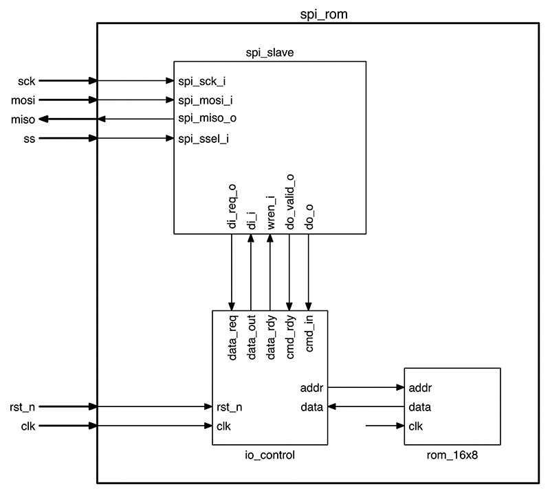
FIGURE 1. SPI serial ROM block diagram.
As you can see, the top-level module (spi_rom.v) has six signals. The standard SPI signals are wired directly to the SPI slave module, and the clock and reset signals are wired to the I/O control and ROM modules. Pretty simple!
How Does This Work?
Don’t worry, I wasn’t going to leave you hanging. Let’s talk about how the I/O control module functions, which is the brain of the SPI serial ROM. At its core, the I/O control module has two registers: one for the SPI slave data request signal and one for the ROM read address.
The data request register is used as a positive edge detector for the data_req signal. Normally, the data request signal is low. However, if the SPI slave module requires data, it will send a pulse to the I/O control module which is two clock cycles long, as shown in the SPI slave source (spi_slave.vhd). The logic for the edge detector is basic and is shown in Figure 2.
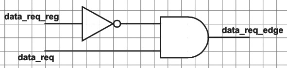
FIGURE 2. Edge detector logic.
The truth table is shown in Table 4.
| data_req_reg |
data_req |
data_req_edge |
| 0 |
0 |
0 |
| 0 |
1 |
1 |
| 1 |
0 |
0 |
| 1 |
1 |
0 |
TABLE 4.
We can’t very well talk about decoding a command without first discussing our command format. The I/O control module will accept an eight-bit byte in the format as in Table 5.
| Bit 7 |
Bit 6 |
Bit 5 |
Bit 4 |
Bit 3 |
Bit 2 |
Bit 1 |
Bit 0 |
| Command |
Address |
TABLE 5.
As you can see, the upper nibble is the command and the lower nibble is the ROM read address. The module will respond to only one command — 0x1 — which sets the ROM read address as discussed earlier.
So, how do we decode a command? First, the module checks if a command has been received (cmd_rdy). If it has, we verify that the upper nibble is equal to 0x1. If it is, we transfer the address stored in the lower nibble of the received command to the ROM read address register in the module. Pretty easy, right? However, there is one catch.
How do we respond to subsequent read operations? If a command is not ready and the SPI slave module is requesting more data (data_req_edge), then we will increment the ROM read address register by one. The logic diagram is shown in Figure 3.
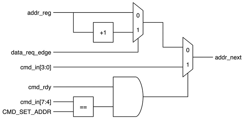
FIGURE 3. Command decoding logic.
Let’s Test!
With everything glued together, it’s time to verify operation of the SPI serial ROM. I wrote a test bench (spi_rom_tb.v) which essentially “bit bangs” the SPI protocol at a 1 MHz SPI clock rate to test our module.
Two operations we need to test are the command decoding logic and the incrementing of the ROM read address for subsequent reads. The test sequence is as follows:
- Initialize the SPI bus to an idle state.
- Send a command to the SPI serial ROM to set the ROM read address to 0x4.
- Read two bytes from the SPI serial ROM.
Let’s take a look at Screenshot 1 to verify our SPI serial ROM operation.
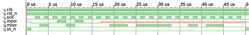
SCREENSHOT 1. SPI serial ROM test bench.
Our module first receives the command 0x14 which sets the ROM read address to 0x4. At the same time, the SPI serial ROM is sending the ROM data from address 0x0 (the initial reset value for the ROM read address) to the SPI master. This data is the letter ‘H,’ or ASCII code 0x48.
The next two read operations output data from addresses 0x4 and 0x5, which are ‘o' and ‘,' (ASCII comes 0x6F and 0x2C). Everything works as advertised!
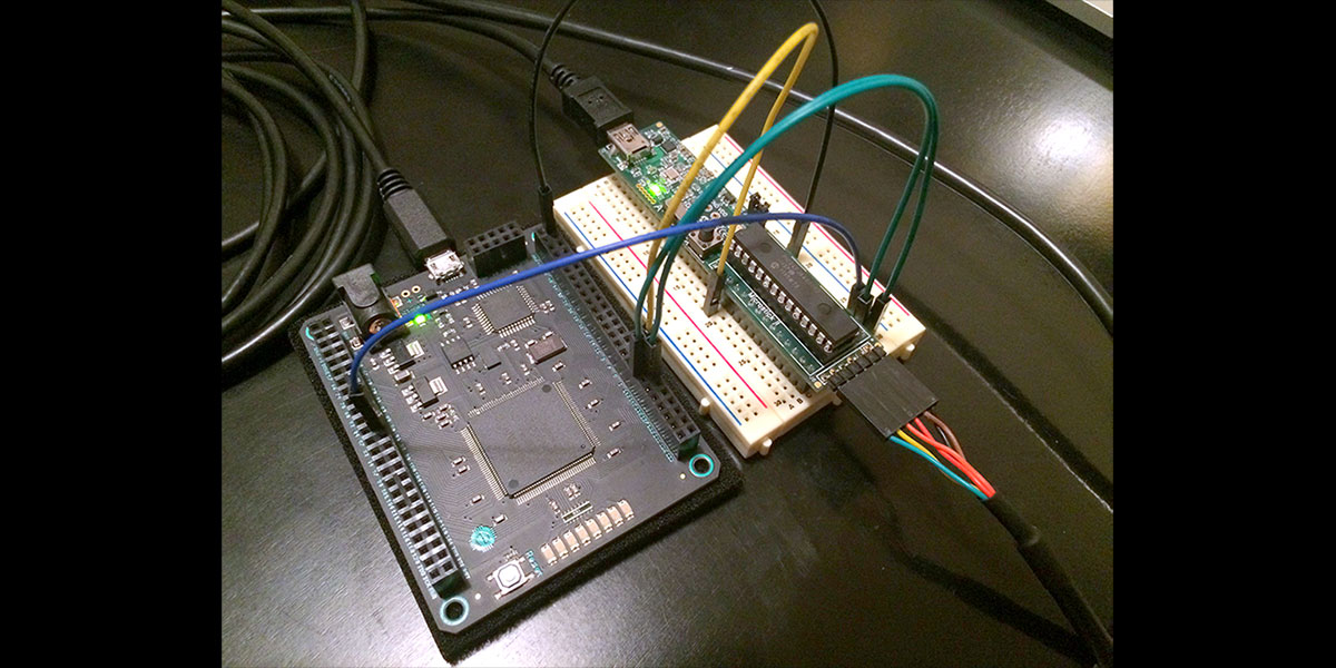
Let’s get this loaded on the Mojo V3 and test it with our Microstick II.
Hardware Time
The code for the PIC24FJ64GB002 on the Microstick II and the Mojo V3 is available for download at the article link. I soldered a right-angle header to J6 of the Microstick II, which connects to pins 21 and 22 for use with the UART module. You will need a 3.3V TTL serial cable to interface with your computer. I used a SparkFun FTDI cable (DEV-09717) and the SerialTools software (available from the Apple App Store) for my testing. Connect the Mojo V3 and Microstick II per Table 6.
| CONNECTION |
MOJO V3 PIN |
MICROSTICK II PIN |
| SCK |
93 |
18 |
| MOSI |
142 |
17 |
| MISO |
143 |
16 |
| SS |
144 |
3 |
| Ground |
GND |
27 |
TABLE 6.
The test software is simple to use. It accepts three commands:
d — Dump ROM contents to screen.
r — Read byte from current ROM read address.
a=addr — Set ROM read address to <addr>; a base-10 number from 0-15.
You can see from Screenshot 2 that everything works as expected.
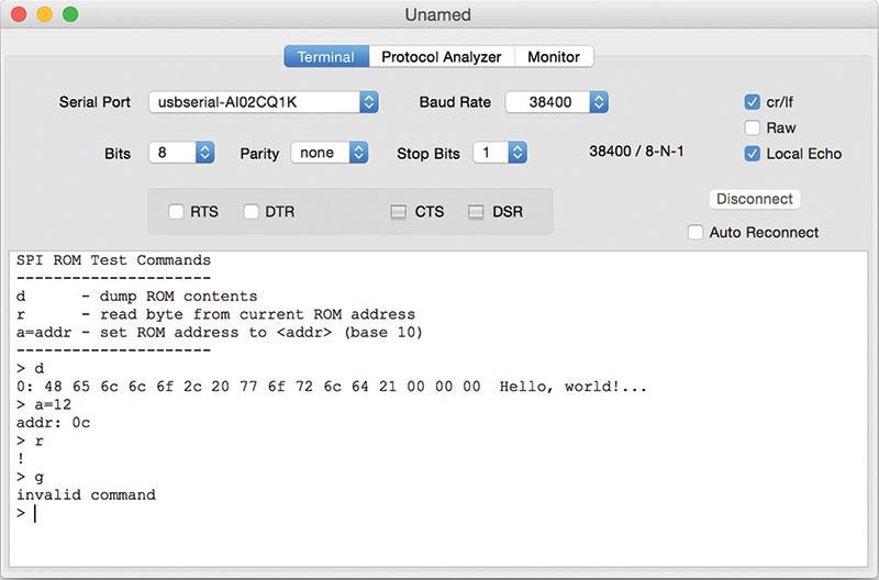
SCREENSHOT 2. SPI serial ROM test.
Where Do We Go from Here?
The OpenCores website has many different cores available, as we discussed at the beginning of the article. One neat feature to explore is the Wishbone Bus. This is an open source bus architecture specifically designed to facilitate communication between IP cores on an FPGA for SoC design. Many of the cores on the site use the Wishbone Bus. Take a look around and find something to hack with.
Until next time, I hope you continue to enjoy the interesting, albeit complex world of FPGAs! NV
Resources
OpenCores.org SPI Master/Slave Interface
http://opencores.org/project,spi_master_slave
Embedded Micro Mojo V3
https://embeddedmicro.com/mojo-v3.html
Microchip Microstick II
www.microchip.com/Developmenttools/ProductDetails.aspx?PartNO=DM330013-2
SparkFun 3.3V FTDI Cable
www.sparkfun.com/products/9717
SerialTools
https://itunes.apple.com/us/app/serialtools/id611021963?mt=12Wishbone
Bus
http://opencores.org/opencores,wishbone
Downloads
What’s in the zip?
Source Code