Every bench needs a power supply to fully complement the rest of its test equipment. I consider this to be just below the DMM in essential test equipment. The question arises, though, as to what type of supply and what features should be incorporated so as to make it as universal as possible.
Background
I have designed and built a dozen different power supplies over the years, but recently I built the one presented in this article. It is the culmination of many years on the test bench, which I feel will cover most situations without going to ridiculous extremes.
When I started this design, I set down certain parameters that I thought were necessary and threw out some that I felt were of too limited use to warrant the extra circuitry and expense. I based these decisions on previous supplies I had built. Some of my objectives were the following: smallest physical size possible so as to take up minimum bench space; separate analog and digital supplies with floating grounds; at least two analog supplies with easily variable voltage; full metering on both these supplies; and last but not least — good regulation and stability.
The final design came out something like this: dual 0-20V @ 1A; 5V fixed @ 1A; no-load/full-load regulation <10 mV; RMS ripple < 0.5 mV; and simultaneous voltage and current metering on both variable supplies. This gave the capability for design/repair of all low power control circuits, but still have enough “oomph” for mid-power circuitry.
From previous experience, I have found that dealing in high-power circuits (which doesn’t occur that often), the requirements for that power are all over the place. It would be difficult and expensive to design a supply to handle all these situations. At present, I have only one high-power supply — a 150 watt, 13.2V unit for standard mobile use (auto, marine, etc.). For the occasional circuits that I build under the high-power heading, I construct a supply just for that device and its particular needs.
Since all outputs are floating with respect to grounds, this can be set up for ± supply voltages (my preference) for analog circuitry and still have a digital 5V source available. Also, all the supplies can be “series-ed” together to provide over 45V at one amp for higher power when needed.
Because of limited panel space due to the unit’s relatively small size, I deleted some features that others might consider essential. One of these was current limiting. I have rarely experienced much benefit from this. Whenever I have accidentally shorted something on the breadboard, usually the discharge of ‘onboard’ capacitance will burn a device out in short order. With dual metering for voltage and current, I can constantly monitor this when the circuit is powered up. Upon initial power-up or any circuit changes thereafter, I can slowly bring up the voltage to the desired level while monitoring the current for unusual excess. As far as protection to the power supply itself, the IC regulators have built-in overload and thermal shutdown.
In the past, my designs have incorporated a lot of discrete circuitry for regulation, etc. Since this unit would have a maximum rating well within the capabilities of readily-available IC regulators on the market, I decided to check them out as to their claims. They all lived up to their specs and performed as well as anything I had designed previously. Their only shortcoming was the lack of provision for remote voltage sensing, but I figured I could live with that by up-sizing my connection leads and the fact that I would only be dealing with a maximum of one-amp loads.
This article will deal with the power supply as built, but will also be interjected with a lot of options and general guidelines for power supply design. To start with, I had the option to go with a linear design or a switchmode design. The linear design pros are, in general, better line/load regulation and less ripple. The switchmode pros are better efficiency and less weight. The advantages of the switcher were of no consequence here, as we do not need mobility or great efficiency in this situation. The last thing one needs on a test bench is a source of EMI, which the switchers are prone to produce!
For the analog supplies (0-20V), I chose LM317K regulator chips with a TO-3 case for improved heat transfer ability (more on this later). Most of this design is pretty much right out of the book and you can Google LM317 (head for National Semi on this page) for a lot of additional information. The 5V fixed supply is based on simple 7805 design.
Theory of Operation and General Guidelines
Most of this discussion on circuit theory, options, and some general guidelines in linear power supply design will refer to the schematic in Figure 1.
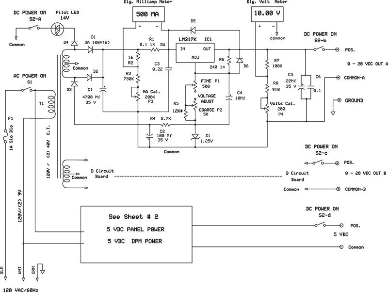
FIGURE 1.
To begin with, the heart of the supply is the main transformer(s). Once the required output voltage and current are determined, design of the raw B+ section can proceed. In this unit, I wanted slightly over 20.0 volts at a full load current of one amp coming out of the regulator chip (LM317). These regulators need a minimum of three volts across them (Vin-Vout) for proper operation. The valleys of the input ripple plus the average DC must remain high enough to support the regulator’s required three-volt differential, and puts the most strain on the raw B+ at full load current. Also, one must consider line voltage sags which further necessitates an increase in raw B+ to cover these situations.
All these factors that require an increase in raw B+ for reliable operation are known as “headroom.” Headroom is the available B+ (pure DC component) under worst-case conditions as compared to the B+ needed under ideal conditions. Regulators love a lot of headroom to cover all situations encountered and still operate reliably. Regulators also hate a lot of headroom due to the increased voltage across them, which increases wattage dissipation, which increases internal junction temperature and, if it goes high enough, could eventually destroy it. So, as is the usual case with electronic designs, we are faced with tradeoffs.
In this supply, I have stated that we need 20 volts of regulated output plus a minimum of three volts differential under any load. This supply also has an RMS ripple of 0.6 volts at full load. That means the negative peak ripple (1.41 x RMS) will dip the average B+ by 0.85 volts. We also still have to consider line voltage sags. These days, power line voltages are pretty stable, so I only allowed for a 5% reduction here. Adding all these factors (differential, ripple, and line sag), we need 25.0 volts for worst-case conditions, which would be under full load current, in regards to raw B+. In transformers of the VA range used here, the voltage would rise about 20% under no load conditions and will produce a raw B+ of 30 volts at that point. This is the minimum headroom at idle.
A general rule-of-thumb when designing full wave rectifiers that are feeding a capacitive input circuit is to size the transformer secondary current at 1.5 times the filter capacitor’s average DC output current. This is due to the high charging currents needed to maintain the capacitor at peak or near peak voltage. Assuming a one volt drop (or two volt for bridges) across the full wave rectifier, we need a peak voltage of 31 volts to each rectifier from the secondaries. This would require a transformer secondary of 22 volts RMS (44 volt center tapped) and a current rating of 1.5 x 1 amp (the DC output current) or 1.5 amps.
I was fortunate to have salvaged one of these transformers from one of my obsolete supplies — a 120V primary with a pair of 44 volt center tapped secondaries at 1.5 amp each. Although these transformers are available, you may find them pricier than the common ‘garden variety‘ 24 volt secondary ones. With these (assuming you couldn’t find a 48V with a center tap), you can substitute a full wave bridge circuit in lieu of the half wave rectifiers. Just make sure the current ratings are as mentioned.
Can’t find one with dual secondaries? Then use two single transformers — one for each variable supply. Two will take up more cabinet space, but not much more. If you choose to make your supply for higher/lower maximum outputs, then size your transformer accordingly. The main idea here is to allow adequate headroom for the regulator, but no more than necessary, to reduce wattage dissipation at that point and the subsequent increase in heatsinking.
One note of CAUTION here! I show a 35V rating for C1,C2 in the Parts List based on a 22V transformer secondary. If you choose to go with a 24 volt or higher secondary, you will need to increase this rating to 50 volts as it puts you just over the limit. And while I am on the subject of C1, although I usually figure about 2,000 µF/amp for input filtering, I went to 4,700 µF on these supplies in order to reduce ripple and yield more headroom above the regulator.
The LM317 regulation circuit is pretty much right out of the book, so I will only run through a quick explanation of how it works. The voltage across the output pin and adjust pin is internally set at 1.25 VDC. A resistor placed across these points will create a constant current source at the Adj. pin junction and that current will be determined by the value of R6. This constant current will be returned to raw B+ through the regulator’s output pin. The data sheets call for a minimum of 5 mA quiescent current through the chip for reliable operation. Since the current through R6 is, for the most part, the regulator’s operating current, R6 was chosen at 240Ω to allow for a 5.2 mA flow to satisfy that requirement. This is also the constant current that will flow from ground up through the voltage adjusting resistance P1,P2. A 1% resistor is used here, not so much for accuracy, but for stability. When P1,P2 are added to the circuit at the constant current point, they will vary the voltage by virtue of their chosen resistance setting. The output will track this voltage plus the constant 1.25 volts (adj. pin to output pin).
However, when P1 and P2 are at zero, the regulator still puts out 1.25 volts. In order to take its output to zero volts, this voltage has to be cancelled. This is where Z1 comes into play (a precision 1.225 volt Zener) by developing an almost exact voltage of opposite polarity. Its circuit consists of negative half wave rectifier D3, filtered by C2 and current limited by R4.
Now, when P1 and P2 are at zero, a negative 1.225 volt level is presented at the current source point and adding this voltage to the positive 1.25 volt constant of the regulator equals zero volts on the output or nearly so. On my unit, I have 0.015 volts and 0.019 volts, respectively, on the variable outputs at “zero” setting. Going back to the voltage adjusting pots P1,P2, their values are determined by two things: the desired output voltage of the regulator and the constant current source. Again, I’ll use this unit as an example.
The constant current was set at 5.2 mA as previously described. Also, since I am taking the low end of the adjustment string to a -1.225 volts which almost nullifies the regulator’s constant of +1.25, the output voltage will track the exact voltage drop across P1 and P2. For a maximum output voltage of 20.0 volts, we need a 20.0 volt drop across P1,P2 and — according to Ohms law — R=E/I = 20/0.0052 = 3850 ohms total.
From past experience, I knew that a single turn pot would not give a smooth enough voltage adjustment for this great of range. It would need about 10 times as much travel for smooth transitioning. I was faced with two choices: a 10 turn adjustment pot or two pots with a 10:1 ratio. A 10 turn pot is too expensive and time-consuming for repeated adjustments, so the combo unit was the clear choice here. These pots should have a resistance ratio of about 10:1. I chose 5K and 500 ohms based on the resistance calculated. In practice, the fine pot is normally left at its midpoint and then tweaked after the coarse pot has set the approximate output desired. This now allows for a fine adjust of ±1.25 volts — a very optimum span.
With the fine adust pot (500 ohm) set at its midpoint and putting 250 ohms into the resistance string, this is subtracted from the 3,850 ohm total previously calculated and leaves us with 3,600 ohms to add for P2. Since the nearest standard pot is 5K, it will have to be shunted to attain the value we need. This is accomplished with R5 (12K) and is calculated based on a 5,000 ohm pot. Bear in mind, most pots have a ±20% tolerance and R5 will have to be adjusted as required (hence, the asterisk on R5).
With P2 (coarse) at maximum and P1 (fine) in its mid position, the voltage output will be 20.0 volts, and P1 will allow for a fine adjust of ±1.25 volts throughout the total range. With P1 and P2 set at minimum, the voltage output will be zero or nearly so. One additional note is that there is a small error current flowing through the P1,P2 string and into the regulator’s adj. pin. This is approximately 50 µA and has been omitted from prior calculations for simplification and because it is of little consequence here.
C3 is added for input bypassing and stability insurance. D5 is a protection diode and will shunt any external capacitive discharge around the regulator rather than through it; in any event, causing a more positive voltage on the regulator output than its input. C4 gives much improved ripple rejection and D6 prevents unintentional C4 discharge through the IC, again shunting these currents around the regulator via D5. C5 and C6 are added for improved transient response.
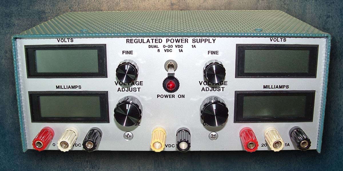
As for the LCD panel meters, I selected the smallest I could find (but still maintain adequate character height for readability) due to limited front panel space. They are all 200.0 millivolt meters. The voltmeters are set up for 20.00 volt operation by proper decimal location and input scaling. R7, R8 are the scaling resistors and P4 is added for calibration. These trimmers are small and cheap and are much more accessible than the panel meter’s internal calibration pot.
The current metering presented a small problem. I wanted to measure 0-1 amps in milliamp steps. This equates to 100 µA/mA since this is a basic 200.0 mv voltmeter (no decimal display is used here). The shunt required for this conversion is 0.1 ohms (R1). I could not add this into the positive output line as there is no provision to keep it in the regulator’s feedback loop.
This would have presented an increasing regulator load current error. For that and other reasons, I did not want it in the negative output either. However, it could be added ahead of the regulator where its voltage drop would be of no consequence. That location presented one other problem though, and that was, even with no load current, there is still the regulator quiescent current of 5.2 mA flowing through this point. This had to be dealt with as even with a 5 mA load current, the meter would show over 10.2 mA — a 100% error at this point.
The solution was to offset the quiescent current and that is the function of R2, R3, P3. Since 1 mA is read for every 100 µV developed across the shunt, a negative 520 µV offset had to be applied to the panel meter’s positive input lead. The values of those components provide just that, so that at no load the quiescent current is exactly cancelled out giving a meter reading of 0.0 mA.
Even though the raw B+ voltage sags at full load and introduces an error in this divider string, it only amounted to a 1 mA error at the full load of 1,000 mA. This error is far beyond the panel meter’s accuracy and can be ignored. The second variable supply is not shown in detail on the schematic because it is a carbon copy of the first one. Just bear in mind, you will need double the components shown to complete both supplies. A diode (D4) to power a 14V LED panel light is attached to one of these supplies to indicate DC power on/off. You will notice I have incorporated a four pole-single throw switch for all DC supplies and the indicator light. When I switch off DC power to a circuit, I want just that — no power! By merely switching off AC power, there is a bleeding off DC voltage present at the panel jacks. This could hang on a long time for light loads. Other reasons for separate AC and DC power switches are to eliminate transients presenting themselves at the font panel jacks upon AC power up/power down, which can occur at the first few milliseconds of AC switching.
Another reason is that when using a negative reference voltage such as Z1(-1.225V) for the regulator and due to unequal charge discharge times of C1, C2, a 1.5 volt step-up in voltage can occur upon AC shutdown only. This is not an easy problem to overcome to cover all situations. Again, DC switches block this undesirable occurrence.
All my power supply designs have incorporated separate AC and DC switching for these and also to give you a setup procedure while the DC power switch is off, as the metering will still be active. If one were to just drag this supply to the test bench for a couple of hours at a time and then return it, there really wouldn’t be any need for an AC switch — just plug and go! But for my use, this supply will become a permanent fixture on my test bench, so I decided it needed AC switching.
Let’s discuss the five volt supplies that are shown in Figure 2.
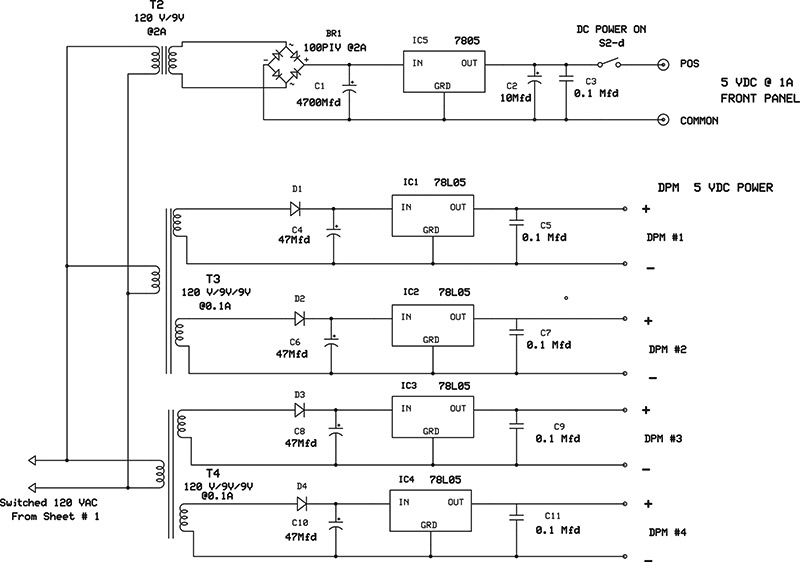
FIGURE 2.
There are five of these, but it’s not as bad as it sounds. There are some options here. The first of these is the 5V at 1A front panel supply. This is so straightforward, it almost needs no explanation. T2, BR1, C1 provide raw B+ to the regulator chip IC5 (7805), which then does a fine job of regulating it to +5 VDC. T2 has a single 9 VAC secondary at 1.5 amps and was chosen for minimum voltage differential across IC5 for reduced wattage dissipation.
The other four five-volt supplies are for the four front panel meters. These are all meters requiring isolated power supplies. Two of these supplies could be eliminated for the front panel voltmeters, since the meter’s negative input is connected to common. A 78L05 (TO-92 case) could be connected to the raw B+ supply and power these meters directly from its positive and common. You will need one of these for each supply you are metering. The meters will have to be the type that operate with common grounds (negative input lead and negative power lead tied to common).
Another option is to use only one meter per supply and switch them from volts to amps, with regards to their input leads. These will require isolated power supplies, but only two instead of four. I have to admit that the meters used in this project are by far the greatest cost of constructing it. I wanted the luxury of full metering all the time, however, and wouldn’t have done it any other way.
The four supplies for these meters take up very little room and the total cost for all the components required was just over $5. These supplies need only half wave rectification and little filtering since load requirements are on the order of 5 mA each.
Construction
I built this unit as small as possible, but you may want to open up the overall dimensions slightly. The power supply’s overall dimensions are 9” wide x 3-1/2” high x 6” deep. If you alter the design, lay out all your parts first to get specific measurements for cabinet clearances and dimensions needed before starting construction. When I make up an enclosure for circuits requiring a fair amount of heat dissipation, I usually build it as follows (see Figure 3).
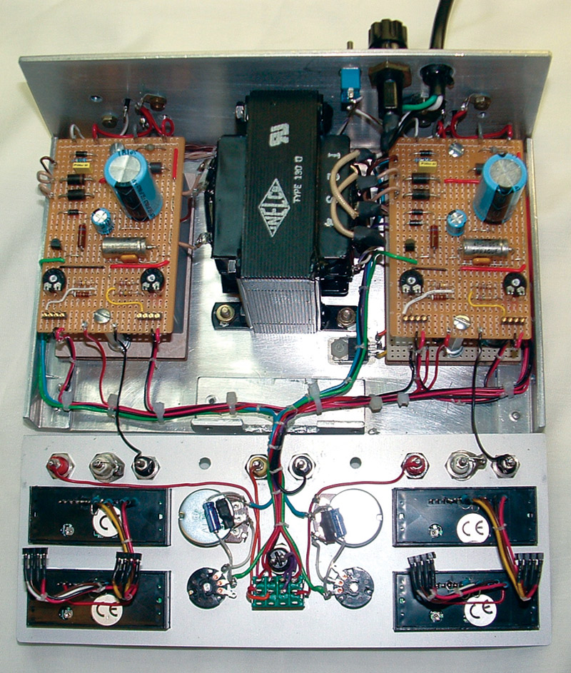
FIGURE 3.
The bottom and back are made of one piece of 1/8” aluminum sheet. A 90 degree bend is formed at the intersection of the bottom and back. In my case, this was a sheet 9” x 9-1/2” with the 90 degree bend 3-1/2” from the long end. This part of the enclosure will also double as the heatsink, eliminating a lot of expense and clutter. Pop rivet three 1/2” aluminum angle brackets to the sides and front of this base, flush with their edges. (In my unit, these were two 6” lengths and one 3-3/4” length.) These will be the attachment points for the front panel and top cover.
Next comes the front panel. This was a piece of 1/16” aluminum cut to 3-1/2” x 9”. Lay out mounting holes at the bottom and transfer these to the front angle bracket on the bottom plate. Drill and tap these for the front panel mounting screws.
Next, the metal cover is formed. Mine was 16” x 6-1/2” with two 90 degree bends, 3-1/2” from the long ends, to form the sides. The 6-1/2” dimension gives the cover a little overhang on the front and back of the enclosure. Drill two mounting holes at the bottom of each side. Align the cover to the base and transfer those holes to the side angle brackets. Drill and tap these for the cover mounting screws.
Some fitting may be necessary as you are constructing this. Disassemble and then later paint it the color of your choice, but do not paint the 1/8” bottom sheet. Add four feet (can be self-adhesive) and the basic enclosure is done. Strong, functional, attractive, and simple, to boot!
At this point, the major components can be installed. Make sure you have allowed ample room and clearance in regards to overall dimensions for the components you have selected. I installed the main power transformer (T1) in the rear center of the bottom plate. This is a logical mounting point and gives the unit good balance. On either side of T1 are two circuit boards spaced and stacked on standoffs, and measuring 2-3/8” wide x 3-1/2” deep. (That will be four boards total.) To the left side of T1 is the five volt panel supply transformer T2, a low profile type mounted to the bottom board. Standoff mounted, the upper board is one of the 0-20 volt (A) boards.
To the right side of T1 are the five-volt supply regulators along with T3, T4, and is the bottom board. As withthe left side, the mounted standoff is the other 0-20 volt (B) board. The rear panel receives two LM317K ICs mounted directly behind their respective regulator boards. The 7805 (IC5) chip is mounted to the bottom plate near the front left hand corner of its regulator board. F1, S1, and the line cord input are mounted through the back panel wherever it’s convenient. The front panel components should be laid out in a nice symmetrical order and then machined. Watch for clearance here to interior components!
For front panel labeling, I have been experimenting with various escutcheons. Recently, I have been using some of the CAD programs from PC and front panel manufacturers. Any CAD program will work as long as it gives you a reference point, precise layout cursors, and the ability to add text. For this panel, I used the free CAD program (Front Panel Designer) from Front Panel Express LLC to lay out and label it. From there, you have two choices: immediately email this to the manufacturer for production or make up your own.
Figure 4 shows the escutcheon I made up from the CAD program.
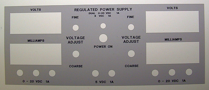
FIGURE 4.
One click of a tool button and you can hide lettering and show layout points for machining the panel. These files will print out to exact dimensions. When I make my own escutcheon, I print out the image of Figure 4 to matte photo paper and then double coat it with Krylon Crystal Clear Finish. Let dry and apply to the front panel with 3M spray adhesive. Hole trim out can be done before or after. For this project, I treated myself and had the manufacturer make up the panel. Pricey, but they do one beautiful job. However, the photocopy method does produce a very professional front panel look, especially with black print on a natural aluminum background.
One last note — the particular panel meters I used were chosen for their small panel mount size since panel space was at a premium. I also chose these with the isolated power option. For some reason, I seem to get better low end stability with isolated power supplying these meters. A 4 pin SIP header was connected to the meter leads via 3” #24 gauge wires, and a matching 4 pin SIP socket was soldered to the front of the board. This gives easy install/removal of the front panel.
Heatsinking Details
Any article on linear power supplies would not be complete without some discussion on heatsinking. A lot of readers are aware of the need for heatsinking but are not familiar with the details of requirements. Heat transfer — as simple as it sounds — can be an extremely complex science, so I will try to keep this discussion simple.
To begin with, all materials have a given rate of heat transfer, which is their ability to dissipate heat generated within them. This ability is known as thermal resistance and is shown as the Greek symbol theta (θ). This will be shown here as Tr (thermal resistance) and actual temperature as T. The lower this quantity is, the lower the Tr, and hence, the greater rate of heat transfer. The rating is given as degrees C/Watt and is the rise in temperature in degrees Centigrade for one Watt of dissipation within a given object. The lower the number, the better the dissipation factor. A loose electronic analogy would be the discharge rate in an R/C circuit, with charge being analogous to heat and R representing Tr. The lower the R is, the more rapid the discharge rate or heat dissipation is.
We start our calculations with the manufacturer’s maximum rating for a semi’s junction temperature. For almost all commercial grade semiconductors, this will be 125 degrees C (150 for military). This means that even operating at worst-case conditions, we must keep that device under that temperature, preferably under 100 degrees C (100 C is not always possible or practical).
Two factors dominate the semiconductor junction temperature rise: the wattage developed across the device and the Tr to the ambient air surrounding it. I will use this supply as an example. The first hurdle we must cross is the Tr of the junction to its case. This is noted as Tr j-c. I chose the TO-3 version of the LM317 because it has a lower Tr j-c than the TO-220 package. The manufacturer specifies a Tr j-c of 2.3 degrees C/W. This means that for every watt of dissipation at the junction, the case temperature will rise by 2.3 C. We always want to look at the worst case here to determine maximum temperature rise. In this example, I will use a near worst-case example of five volts output at a one amp load. The raw B+ at this point is approximately 25 volts, and by Ohms law, we have 25V-5V x 1.0 amp or 20 Watts of heat dissipation within the regulator chip. The 317 case temperature will rise to 2.3 degrees per Watt or 46 degrees C for our 20 W. This is a given we have to live with, but from this point on, we do have some control.
The next hurdle to cross is the Tr of the insulating material between the case and its mounting surface. This is noted as Tr c-s (thermal resistance of case to heatsink). This is almost zero if the case is mounted directly with no insulator. If the case is not electrically isolated from the chip, we have to use an insulator, as is the situation here. I used mica insulators and high quality thermal grease, in which the manufacturer specifies a Tr of 0.35 C/W.
One word of caution — NEVER use production type self-adhesive insulators as they are terrible and seem to perform even worse with thermal grease. Also, I would like to mention at this point that the heatsinks mounting surface should be perfectly flat with no burrs from drilled holes. When insulated like this, mounting is achieved the easiest with nylon screws and nuts.
The last hurdle to cross is the Tr s-a (thermal resistance of the heatsink to ambient air surrounding it). Up to this point, we have a Tr j-c of 2.3 C/W and a Tr c-s of 0.35 C/W for a total of 2.65 C/W and a semiconductor dissipation of 20 W. The temperature rise at the heatsink point-of-contact will be 2.65 C x 20 W or 53 C. Conversely, the semiconductor junction will be 53 degrees C hotter than the heatsink at this point, and if we were running the part at the maximum temperature of 125 C, that means this contact point would now be 125 C -53 C or 72 C.
Bench test equipment is normally used in an environment not exceeding 25 C (77 F) and this is as low as the heatsink temperature can go. The heatsink cannot be allowed to rise in temperature more than 47 C (72 C - 25 C) in order to maintain the maximum junction temperature. Heatsinks are rated by their thermal resistance Tr s-a (sink to ambient air) which is given as degrees C/Watt. Since we are dealing with 20 W and plugging this into the formula, we have 47 C/20 W or 2.35 C/W. This is the minimum heatsink Tr we can get away with. In practice, we would want a heatsink with less Tr for a greater margin of safe operation, probably on the order of 1.5 C/W. This would reduce the maximum junction temperature to 108 C for worst-case situations.
From here, you would look up a manufacturer’s heatsink for this rating and it would probably be fairly sizable. Also, you need one for each 20V supply. As a matter of interest, the manufacturer cautions against too much heatsinking on the 317 so that they can reach their thermal shutdown temperature when normal overload occurs.
From past experience, I knew the heatsinking capabilities of the chassis used in this unit would be adequate, so I didn’t bother with precalculations. Post construction tests bore this out by measuring case temperatures at near worst-case for the variable supplies running individually and normal case tests with all supplies running concurrently.
These tests were at full load current and case measurements taken after one hour of operation. The junction temperature was computed by the case temperature, Tr j-c and wattage (20 W) to arrive at a figure for this. The variable supplies were about 115 C, which is just about perfect in regards to overload vs. thermal shutdown. The five volt fixed supply was at 69 C. Even though the TO-220 case of the 7805 has a higher thermal resistance, it runs with much less wattage across it, hence the lower junction temperature.
With all supplies running concurrently at 20V-5V-20V and series up to a one amp load current, the junctions were 65 C - 80 C - 65 C, respectively. This is well under the maximum operating temperatures of 125 C. These were tested with the cover in place and with no ventilation holes. I may add vents at a later date, which would undoubtedly improve these readings.
The current rating on this unit is very conservative and will actually output closer to 1.5 amps, before dropping out of regulation. However, it wouldn’t be advisable to do this at low voltage settings for more than a couple of minutes due to heat dissipation. At higher voltage settings, it can be longer (it all relates back to headroom).
Conclusion
This supply has been in service for several months now, and has performed flawlessly. It has also been very user-friendly. If you do not currently own a bench supply, build this one. After a few usages, you will wonder how you ever got along without one. I hope that even if you don’t build this unit, you will have gained some helpful pointers that will be of use in similar projects. NV
PARTS LIST
|
| ITEM |
DESCRIPTION |
| 0-20 VOLT BOARDS |
| T1 |
120V primary, dual 44V center tap secondaries @ 1.5A |
| D1,2 |
3A, 100 PIV |
| D3,4,5,6 |
1N4002 |
| C1 |
4700 µF/35V * |
| C2 |
100 µF/35V * |
| C3 |
0.22 µF |
| C4 |
10 µF/35V |
| C5 |
22 µF/35V |
| C6 |
0.1 µF |
| R1 |
0.1Ω 1% 3W |
| R2 |
16Ω |
| R3 |
750K |
| R4 |
2.7K |
| R5 |
12K * |
| R6 |
240Ω 1% |
| R7 |
100Ω |
| R8 |
910Ω |
| P1 |
500Ω |
| P2 |
5K |
| P3 |
200K |
| P4 |
200Ω |
| Z1 |
1.25 volts reference |
| IC1 |
LM317K |
| FIVE VOLT SUPPLIES BOARD |
| T2 |
120V primary, 9V secondary@ 1.5A |
| T3,T4 |
120V primary, dual 9V@ 65 mA secondaries |
| C1 |
4700 µF/16V |
| C2 |
10 µF/16V |
| C3,5,7,9,11 |
0.1 µF |
| C4,6,8,10 |
47 µF/16V |
| BR1 |
2A, 100 PIV |
| D1,2,3,4 |
1N4002 |
| IC5 |
7805 |
| IC1,2,3,4 |
78L05 |
| MISCELLANEOUS |
| S1 |
SPST toggle switch |
| S2 |
4PST toggle switch |
| Panel Meters |
200.0 mV |
Downloads
What’s in the zip?
PCB Files