 |
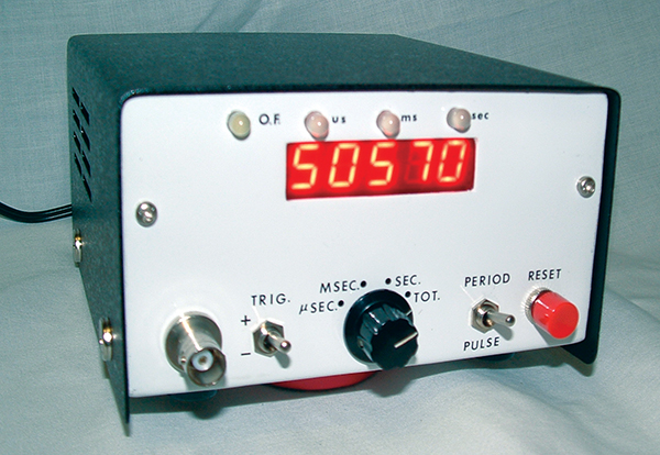
| Front view of the counter. |
For several years now, I have been wanting to design and build a period counter with totalizing function. I finally made time to do just that. My initial design was quite basic, but then I started the what-ifs, and the original design grew to twice its size.
When I finished the first prototype, I sat back and s tudied it. Then I asked myself what would I want to strip to make the design simpler. The answer was, “nothing.” It was very functional the way it stood, and it’s a dandy.
The pleasure and convenience of use in the coming years far outweigh the few extra hours needed in construction. So there: I had what I wanted — another “mighty weapon” to add to my arsenal of bench test equipment. A simplification in design, with a slight loss in overall accuracy, is included near the end of this article for those who prefer to have less wiring to do.
You may be thinking, “Why build a period counter when I already own a frequency counter?” For starters, there are many situations where it’s just more convenient to count electrical signals and read out the actual time (µs, ms, s) rather than frequency. Some frequency counters will also read out the period, but almost all of them fall short for slow repetition rates or long periods between uses. Their lower limit is around 10 Hz.
The counter described here also has additional important features. In addition to its wide range of counts (from one to one billion), it will also capture and display pulse width, either positive or negative. At its extreme range, it will capture and display a single pulse as narrow as 1 µs, even if it only occurred once a day — try doing that with your oscilloscope!
On the other end of its range, it will count rates as slow as 1,000 seconds or as fast as high-speed pulse trains from a function generator’s burst mode of operation. And finally, a totalizing function was incorporated into it to count electrical events and sum them (up to 100,000).
Although operation of counters are similar, they differ in several respects. A frequency counter counts an unknown clock rate of input cycles in a known gate time, usually one second, and displays the count in Hz/sec.
A period counter counts a known clock rate in an unknown gate time (input signal) and displays this as the actual time of occurrence. For this reason, period counters are a little more complex.
This counter will perform the following:
- Period count — One microsecond to 1,000 seconds
- Pulse width — One microsecond to 1,000 seconds
- Totalize — One to 100,000 events
Although measuring pulse width will lose accuracy below one microsecond due to resolution, it can capture and display glitches down to 100 nanoseconds. Totalizing input pulses can be as short as one microsecond or as long as a month. All of the above functions will accept any type of waveform.
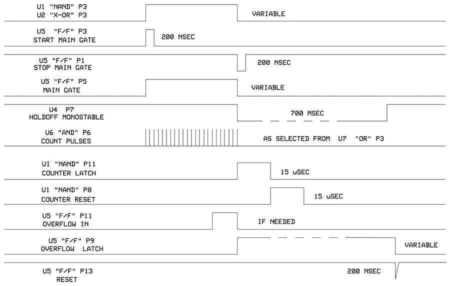
Before we get into construction, I will give a complete theory of operation for understanding circuit operation and eventual troubleshooting, if necessary, upon completion. To aid in this discussion, I am including a timing diagram which will be referred to in the schematic diagram. This will be of use because there is a lot of high-speed sequential edge triggering required in this unit.
 |
| TIMING DIAGRAM |
Theory Of Operation
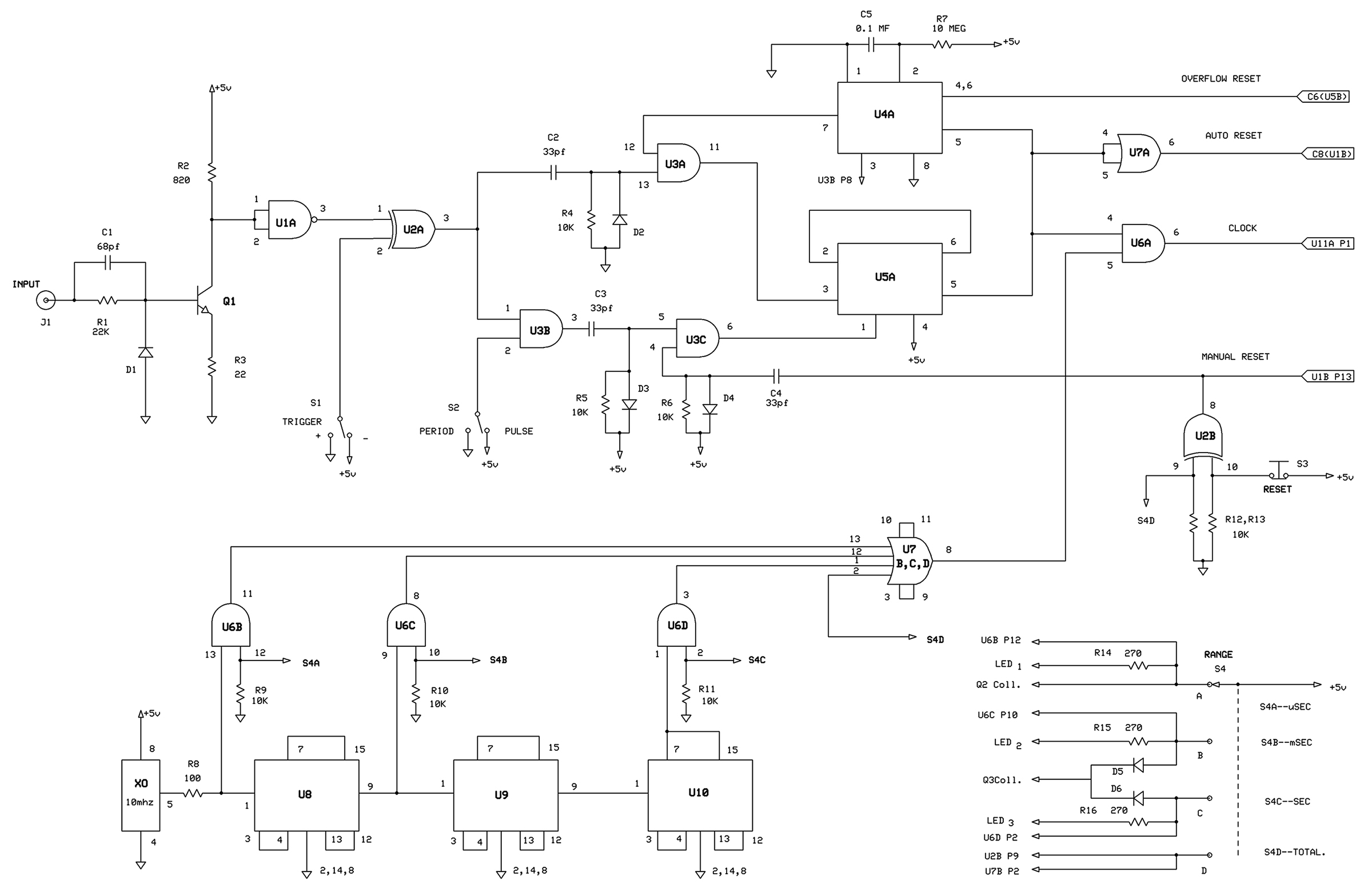
The signal under test enters J1 and is amplified by Q1. R1 limits Q1 base current and C1 aids in high-frequency response. D1 clips negative peaks to protect Q1. This stage has an overall gain of approximately three or four. Its input sensitivity is 1.4 volts peak, which is adequate for all logic families in use today except ECL (0.8 vpp), but that’s beyond the intended use for this design.
The input impedance is 22 kΩ, shunted by less than 50 pF. This circuit produced no noticeable degradation to rise or fall times of the input signal. The input can be of any waveform from 1.4 vp to 50 vp (100 vvp-p). Beyond 50V, you will need an external attenuator. This can be as simple as a resistance divider if extreme speed is not an issue, and it usually isn’t at these high levels.
The output of Q1 drives U1A — a NAND gate with Schmidt-trigger action. The output of U1A is a textbook-perfect rectangular wave, no matter what wave shape or amplitude is input to J1. Only its length will vary, according to the input signal. For this reason, I started the timing diagram at this point.
 |
| SCHEMATIC 1 |
The next stage — U2A — allows for selection of positive or negative edge triggering of the input signal while still maintaining a positive-going pulse as its output, since this is what the circuitry that follows it wants to see. The use of an exclusive OR gate fit the bill perfectly here. A lookup of its simple truth table will bear this out.
The output of U2A is split into two paths: one to start the main gate, F/F, and one to reset the same. Assume for the moment that S2 is switched to period mode of measurement; U3B will block any signals in that path by grounding one of its inputs. The leading edge of the pulse applied to U3A is highly differentiated by C2, R4. This will produce a 200 nanosecond positive pulse to U5A’s clock input (P3). Only the leading rising edges of the input will be seen by this circuit, due to the gate configuration of U3B. U5A is a D type F/F that is wired for toggle operation by connecting P6 to the data input P2.
Now, starting from its reset position, Q (P5) will go high with the first rising edge of the input pulse, low with the next rising edge, and so on. This produces a main gate pulse coincident with the period of the signal under test.
Now, assume S2 is switched to pulse measurement. U5A starts the main gate action — output goes high coincident with the rising edge of the input signal. But now we have to enable U3B by putting a high on one of its inputs. U3C will now perform exactly as the above U3A did, but with one exception — it will output a 200 nanosecond negative pulse only when the input signal is on its falling, trailing edge.
When U5A sees this negative spike at P1, it immediately resets its output to a low, and thereby aborts its toggle operation. Now the output at this point is an exact replica of the input pulse width. Up to this point at U5A P5, we have an exact gating pulse based on either period or pulse width and triggered from either positive or negative edges. Also from this point the gating pulse diverges in three directions:
- It enables main gate U6A for its duration and allows selected master clock pulses to pass through to the counting circuits of U11A and U13.
- It drives U7A to deliver the necessary timing pulses for latching and resetting of the counters. U7A is a leftover OR gate from a quad IC, and is put to good use here as a buffer to drive the high input capacitance (1,000 pF) of the U1B circuit. Without this buffer, some deterioration of the main gate signal would occur.
- Finally, it triggers U4A P5, which is a dual monostable IC. Its role is that of a holdoff circuit. As soon as we complete one cycle of the main gate pulse, the negative edge triggers P5 and produces a low at the P7 output which disables U3A so that U5A cannot operate again until the monostable times out (700 ms). This action immediately blocks any input pulses from entering U5A’s clock input and keeps it that way. When the holdoff times out, U3A is once again enabled and will operate on the next incoming signal pulse, at which time the whole operation will repeat itself. The reason for this holdoff circuit is to latch the count circuit into the display long enough to read it. Without it, the digits would flicker constantly at higher period rates. The holdoff time of 700 ms is arbitrary and may be changed by adjusting the time constant of C5, R7.
At this point, we will switch from analyzing signal flow through the front end and focus on the time base. The accuracy of any unit is that of its time base and is given as:
Time base error in PPM, ± resolution, ± one display count.
I decided to use a packaged oscillator (eight-pin DIP) as it does not cost much more than a lone crystal — $1.70 for this unit. The manufacturer guarantees ±100 PPM, but of the several units I purchased, they were within 5 PPM at room temperature. This accuracy is far beyond what the display can resolve, almost removing it from the equation.
Since we cannot escape the ±1 digit in the display, accuracy depends almost totally on resolution. The lower the display count, the greater the possible error. For example, with a display of 10, due to resolution error, the actual count could be closer to 9 or 11, a possible error of 10 percent. This would be an extreme case. The higher the count, the greater the resolution, hence the greater the accuracy. The only way to get around this is to add more digits to the display. I stopped at five digits, because I felt I was at a point of diminishing returns. I have checked this unit against an expensive laboratory counter at full display, and it was right on the money!
With that said, we will continue with time base and master clock operation. XO is a 10 MHz oscillator (100 ns), which is divided by 100 (10 µs), and by 100,000 (10 ms) through the divider chain of U8, U9, U10. Three clock rates can be input to U7bcd (10 MHz, 100 kHz, 100 Hz). The fourth input is 5 VDC for totalizing. Selection of these inputs is accomplished by S4. Starting at the top A position, 5 VDC is applied to U6B gate, enabling the 10 MHz clock (100 ns) to pass through U7 to the input of U6A. Also Q2’s collector is energized to light the correct decimal point. At the same time, a front panel LED is lit through R14. This would be labeled usec and its count range will be 0-9999.9 µs.
With S4 switched to B position, the U6c gate is enabled, passing the 100,000 kHz (10 µs) clock rate to U6A. Again, R15 lights the appropriate front panel LED. Also Q3’s collector is energized, shifting the decimal point. This is labeled msec and its count range is 0-999.99 ms.
With S4 in position C, U6D is enabled, passing the 100 Hz (10 ms) clock rate U6A. As before, R16 lights the appropriate front panel LED. The same decimal point is lit as in B position. Diodes D5 and D6 isolate these switch positions from inadvertently being energized from backfeeding. This range is labeled sec and its count range is 0-999.99 s.
Finally, with S4 in position D, all clocks are disabled, and a steady high is applied to U6A. Now we can count the actual gate pulse as one digit per pulse for a totalizing function. Also, the manual rest line is pulled low and kept there, thereby enabling the counters to count and display continuously without resetting and allowing totalizing to occur. One word of caution here — S2 must be in pulse mode when totalizing.
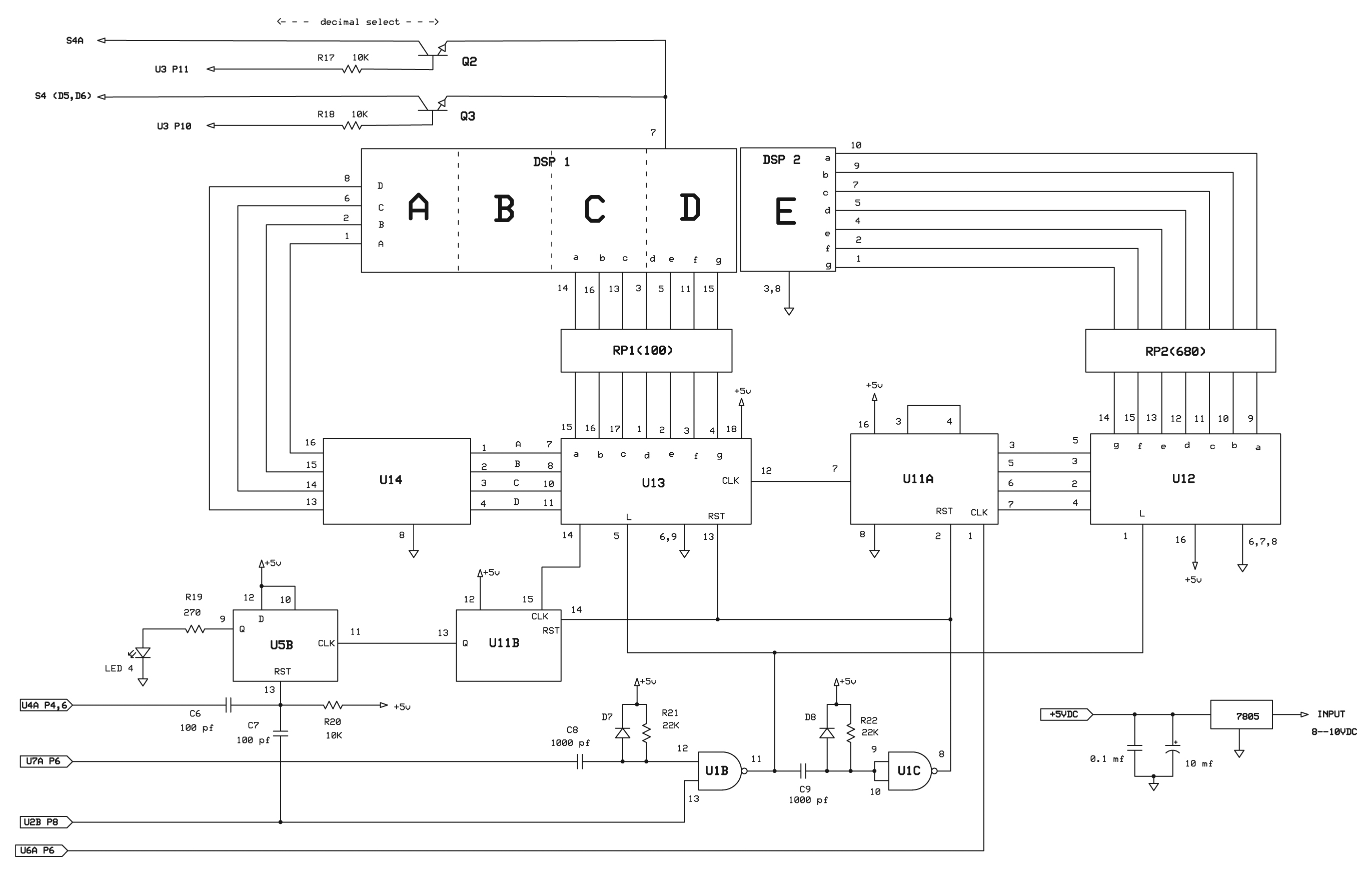
Now we are back to where we left off on the front-end circuitry at U6A. When U6A P4 goes high, the clock rate we have selected will be present at U6A P5 input and passed through to the first counter U11A P1, which is a high-speed decade counter. Its overflow goes to U13, a multiplexed four-digit counter, latch, decoder. When main gate U6A P4 goes low, all counting stops and is stored in the counters. At this point, we have counted a known clock rate in an unknown gate time. When the count state is latched into the display, it will read out the gate time (our input signal under test) in real time.
 |
| The display board. |
For example, let’s say we had selected the S4A µs range and had counted and latched 5,000 clock pulses (10 MHz; 0.1 µs) during the time the main gate was enabled. The display would read 500.0 µs (5,000 times 0.1 µs). This is the period or pulse width from the circuit under test. Backing up just a bit, when U6A P4 went low, the first event to happen was that the counters stopped counting. The same main gate pulse was also coupled through U7A to U1B P12. U1B is a simple one-shot circuit, whose output is dependent on the RC time constant of R21, C8. In this case, it outputs a 15 µs positive pulse when triggered from the trailing negative edge of the main gate pulse. This pulse latches the count state into the display.
 |
| SCHEMATIC 2 |
Also, the trailing negative edge of this pulse triggers an identical circuit, U1C. This is the auto reset circuit. The output of this stage resets the counters to zero and readies them for the next measurement. For manual reset, this line is normally held high. When S3 is depressed, the line goes low, resets the auto reset circuit, and directly clears the main gate F/F through U3C, the holdoff mono. It also clears U5B (overflow latch) through C7. This same latch will also be cleared automatically when the half circuit times out through C6.
As mentioned before, while in a totalizing operation, a constant low is put on the manual reset line by S4 D action. This is needed to continuously latch through the count state from the counter. This presented a problem for manual reset because the reset line was already low! Once again, the exclusive OR gate, U2B, came to the rescue, allowing manual reset to occur regardless of which state that line is in.
There is just one more topic to cover before construction — the overflow circuitry. Without an overflow indicator, ambiguity becomes a problem. When U13 completely loads up the counters and goes into overflow condition, its carryout (P14) sends a signal to U11B, which acts as a sort of decoder. The output of this stage operates a latch {U5B) to light the overflow LED from P9.
One other item that may have piqued your curiosity is the circuit associated with the decimal points. These points on the display are multiplexed with no provision to light them externally. This was quite annoying, and for that reason a decoder had to be added (Q2 and Q3) to light them at the proper time.
Construction
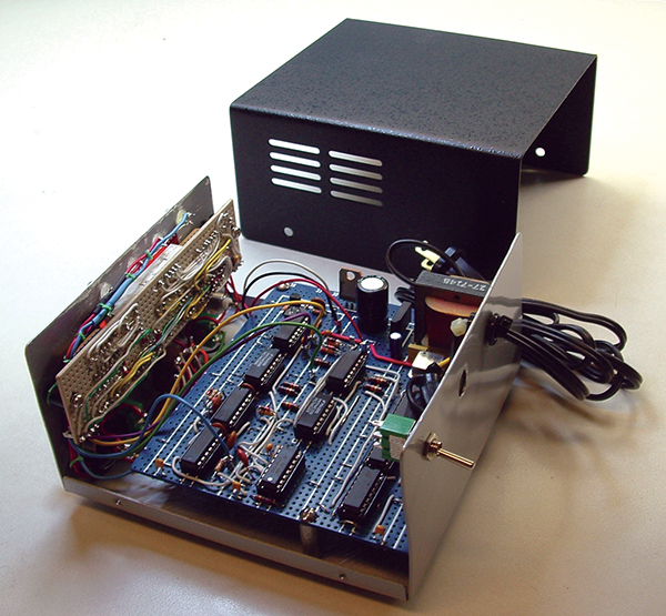 |
| A look at the internal wiring. |
This about covers the theory of operation; now onto construction. I built the display circuitry on a 1-1/4” x 5” perforated board. This board contains both displays, U11, U12, U13, U14, RP1, and RP2. I mounted the board behind the front panel on 3/8” standoffs such that it lined up to a 1/2” x 2-1/2” display window cut into the panel.
The rest of the circuitry, including an AC power supply, was mounted on a 5” x 4-1/4” perforated board, as shown in the internal wiring photo. Everything was installed in the chassis shown in the Parts List. It was a tight fit, and I might opt for the next larger size in this series were I to construct another one. I did not detail a power supply in the schematic, since most constructors use what they have on hand from their junk box.
The properly bypassed, 5V regulator (7805) shown in the print can be driven from any DC source of 7.5-12 VDC. I show the power supply components that I used in the photo on page 48. This was a small 120/7.5 VAC transformer, full-wave bridged into a 1,000 µF ‘lytic to provide an 8V source for the 7805. Power requirements are 5 VDC at 160 mA with all digits lit to 8.
To conserve space, you could use a wallwart type of transformer. Or, if you prefer battery operation, use four AA cells in series with an IN4001 diode. This will give a supply voltage of about 5.5 VDC; no 7805 used here.
Also, for battery operation, you can replace RP1 with a 330 Ω resistor and RP2 with 2,000 Ω. This will cut the current consumption in half (50 mA average) and still give a decent readout. This sort of readout-brightness/current-draw tradeoff comes down to preference, and is thus best determined by the user.
One last item about construction — as mentioned earlier in this text, you can simplify this project (with some loss of overall accuracy) by eliminating U11, U12, RP2, display No. 2, Q2, and Q3. You will end up with a four-digit counter that has no decimal point. The clock input U11A P12 then goes directly to U13 P12. Change the 10 MHz XO to 1 MHz XO, which is shown in the Parts List, and eliminate all front panel LEDs.
The ranges will now be:
- S4A 0-9,999 microseconds
- S4B 0-9,999 microseconds
- S4C 0-9,999 seconds
- S4D Totalize to 9,999 counts
This will require a little more care in use. Without an overflow light, you may have to work down from a slower range to eliminate ambiguity. This modification will also reduce current consumption for battery use. You will also need to change the clock output connections to accommodate these ranges:
- Microseconds — U8 P1 (same)
- Milliseconds — U9 P7
- Seconds — U10 P9
- Totalize — Same
In addition to being a very useful piece of test equipment, this is an interesting and educational project, since it involves many types of logic applications — display circuitry, high-speed sequential timing, etc.
Be sure to ground all unused IC inputs. Take your time wiring it, and double-check your connections (the most common source of errors) as you proceed, and you should have no problems. NV
PARTS LIST
| ITEM |
DESCRIPTION |
ITEM |
DESCRIPTION |
| R1 |
22 kΩ |
U1 |
74HC132 quad NAND gate |
| R2 |
820 Ω |
U2 |
74HC86 quad exclusive OR gate |
| R3 |
22 kΩ |
U3,6 |
74HCo8 quad AND gate |
| R4,5,6 |
10 kΩ |
U4 |
74HC4538 dual monostable |
| R7 |
10 MΩ |
U5 |
74HC74 dual D flipflop |
| R8 |
100 Ω |
U7 |
74HC32 quad OR gate |
| R9,10,11,12,13 |
10 kΩ |
U8,9,10,11 |
74HC390 dual decade counter |
| R14,15,16,19 |
270 Ω |
U12 |
CD14543 four-digit display ctr,dec,drv (Jameco) |
| R17,18,20 |
10 kΩ |
U14 |
ULN2003 npn inverters |
| R21,22 |
22 kΩ |
Xo |
10 MHz ttl osc. (Mouser 520-TCH 1000) |
| |
|
Xo |
1 MHz ttl osc. (Mouser 520-TCH 100) |
| C1 |
68 pF |
S1,S2 |
SPDT toggle switch |
| C2,3,4 |
33 pF |
S3 |
Pushbutton switch NC |
| C5 |
0.1 mF |
S4 |
Rotary switch – four position |
| C6,7 |
100 pF |
RP1 |
14 DIP resistor, 100 Ω |
| C8,9 |
1000 pF |
RP1 |
14 DIP resistor, 680 Ω |
| D1 Thru D8 |
IN914 |
Display #1 |
Four digit, 0.4 inch, multiplexed (Digi-Key 160-1551-5-ND) |
| |
|
|
|
| LED1,2,3 |
10 mA red |
Display #2 |
One digit, 0.4 inch (Digi-Key 160-1533-5-ND) |
| LED4 |
10 mA yellow |
Chasis |
4OUB103 EPD (Mouser) |
| Q1,2,3 |
2N3904 |
|
|