In the midst of all things digital, it seems that the utility of analog mathematical circuits has been shunted aside. This is not surprising. Generally, digital computing has many advantages over analog computing. However, in the realm of microcomputers, some of these calculations are not trivial and can sometimes be downright nasty to implement. So, there are still useful and important applications for analog mathematics in today’s digital world. In fact, the marriage between analog computing and microprocessors (µCs) can be remarkably efficient.
For example, suppose you need to calculate the logarithm of a voltage to stabilize your robot. You could try to perform a direct calculation which would take a lot of time. You could use a look-up table which would use a lot of memory. Alternatively, you could employ some sort of recursive estimation which takes a variable amount of time and fairly complex programming. However, using an op-amp and a transistor you can find the logarithm of your voltage as fast as the op-amp can settle. This article will discuss techniques of analog pre-processing in order to streamline your whole µC system.
Analog Accuracy, Resolution, and Repeatability
The accuracy of a measurement is how close it matches some standard. That is, if the meter reads 1.000 volts the voltage should really be 1.000 volts, not 1.100 volts. Open-ended analog systems usually have an accuracy of a few percent. This initially seems quite bad. But many µC analog-to-digital converters (A/D) use the positive power supply for a reference voltage. This supply can easily vary by a few percent. The situation is much worse if batteries are used. If a voltage reference is employed (a device that provides a precisely defined voltage), then analog and digital accuracy can be about the same (for simple µC systems). However, it is rare for the accuracy of analog systems to be better than about 0.01% (13 bits). More typically, analog accuracies are about 0.1% (10 bits).
Resolution refers to the ability to separate two closely spaced values. Generally, this is defined by the number of digits or bits. An eight-bit A/D has a resolution of 1/256. So, if the A/D reference is 5.000 volts then each bit is 0.0195 volts (5V divided by 256) or about 20 mV. This is pretty bad. Analog systems have “infinite” resolution. That means that there is nothing inherent to the system that limits the resolution. Obviously, no system has true “infinite” resolution. Noise and other factors create a practical limit. But this limit can be very tiny. It is not unreasonable to have analog resolution down to 1 ppm (Part Per Million). This corresponds to about 20 bits in a digital system. (This is seen in ordinary audio recordings. Digital systems of 16 bits are the minimum for Hi-Fi playback. Twenty-four bits and higher are now commonplace.)
Repeatability is the big weakness of analog systems and the big strength of digital systems. Unit to unit repeatability is often limited to a few percent for analog systems (without a reference). Worse, over time and temperature an analog circuit can change by many percent. This is generally the result of component value change. Digital systems do not have this problem.
However, there is a problem associated with analog repeatability when multiple stages are used. In this case, the errors are multiplied by the number of stages (or worse). So, if you are cascading analog math circuits, don’t expect high precision. This is generally not a problem with digital math because the only error associated with multiple operations is the rounding error of half a LSB (least significant bit). If the word length of the numeric values are large enough (16 to 24 bits), this can generally be ignored.
Associated with repeatability is the consideration of noise. Analog systems are susceptible to many sources of noise at all levels. This causes variations in repeatability. Depending on the circuit, this noise may or may not be an important factor. Digital systems are only concerned with noise when it approaches a significant percent of the bit value. Once digitized, noise is rarely a concern. Digital values can be repeated virtually forever without degradation. Analog values (like tape recordings) show a continuous loss of repeatability every time it is reproduced because noise is added every time. However, this repeatability concern is not really a factor here because we are examining analog pre-processing rather than analog reproduction.
Scaling
The simplest analog pre-processing is converting your analog signal to match your A/D. If your A/D has a range of zero to five volts, it will work best if your input signal is in that range. If your input voltage goes from zero to one volt, then 80% of the A/D’s resolution is being wasted. (For convenience and unless otherwise specified, it will be assumed that an eight-bit A/D is available on your µC and that it will operate with an input of zero to five volts and a bit value of 19.5 mV.) This procedure is called scaling. Simple mathematical operations like adding, subtracting, multiplying, and dividing are used.
The simplest scaling problem to solve is when the signal is too large for the A/D. For example, suppose your sensor provides 0 to 10 volts. Here, a simple voltage divider is all that is needed. Figure 1 shows a typical scaling circuit. However, there are a couple of points to address.
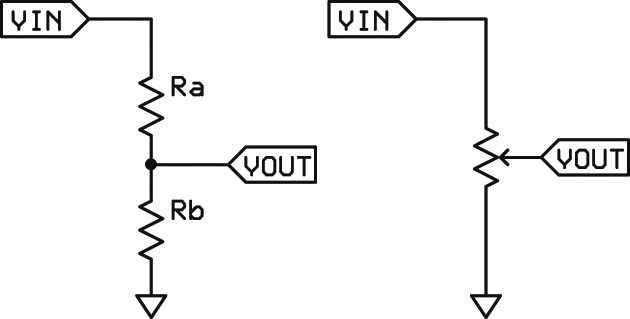
FIGURE 1. A simple voltage divider can be made up of two resistors or a potentiometer. The voltage out is equal to Vin * Rb/(Ra+Rb).
Accuracy depends upon the precision of the resistors. Two 1% resistors can yield a worst-case error of 2%. If the desired divider ratio is not simple, it may not be possible to find exact resistor values (your needs may fall between two standard values). Of course, you can always add additional resistors in series or parallel to obtain exactly what you need. A potentiometer can certainly provide the exact ratio, if you are willing to live with the initial setup effort and the possibility of vibration changing the setting. The formula for determining the resistor ratios is: Vout = Vin * Rb/(Ra+Rb).
More importantly — and more subtly — it’s important to match the resistance values of the divider to that of the sensor and A/D. Most µCs expect to see a fairly low impedance for the A/D input. Typically, this is about 10K. Thus, your divider resistors should be significantly lower than this or else conversion errors can happen. However, your sensor must be able to provide enough drive for the divider resistors (generally a few mA). (Note that if this is a problem with the divider, it is likely there is a problem when directly connected to the A/D, as well.) For added drive, an op-amp can be used to buffer the signal as shown in Figure 2. This allows large resistance values to be used for the divider.
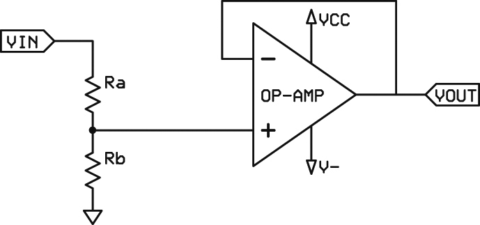
FIGURE 2. Adding an op-amp as a buffer provides more drive to the divider circuit.
Once an op-amp is added, more considerations are necessary. The first is that the input and output range of the op-amp must match the range of the sensor and A/D. Modern rail-to-rail op-amps can come to within one or two bits of zero and Vcc. Normally, this is adequate. Older op-amps may not accept an input value within a volt or so of Vcc (most can accept an input voltage of zero volts) so the maximum input value is reduced. Their output voltages require substantial headroom for both Vcc and ground. For example, consider the popular LM741 op-amp. Its output can’t come closer than two volts to either voltage rail. The LM324’s output can go to as low as 20 mV, but can’t come closer than three volts to Vcc. So, if you are using an LM324 at five volts, the input range is zero to three volts and the output is 0.02 to two volts. (Note this illustrates one of the many reasons why the LM741 and LM324 should never be used for serious work.)
A separate power supply for the op-amp is always useful because it allows you to compensate for headroom problems. Additionally, it can reduce noise that may come from the digital switching in the µC. Figure 3 shows a simple method to isolate the op-amp power from the µC power.
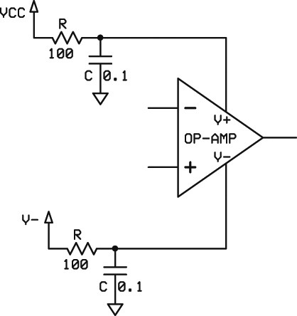
FIGURE 3. Isolating and filtering the power supplies reduces noise to the op-amp. If the op-amp negative supply is ground, then the V- components should be eliminated and the op-amp V- pin should be connected directly to ground.
All of this may seem to be adding more project difficulty than removing it. Proper circuit design demands attention to detail. Examining all the aspects of a circuit is critical for the proper operation of that circuit. It is important to understand the implications of a circuit before implementing it. For example, you know that most µC A/D converters use Vcc as the reference voltage, didn’t you? And that typical three-terminal voltage regulators are accurate to only ±5%. The point is that all the strong and weak issues must be analyzed before you start soldering things together. If you are not familiar with op-amps, it is necessary to explain these points before continuing. This is somewhat similar to examining power-on-reset for a µC before starting a project. There will be no further discussion of op-amp requirements.
Multiplication
Making a signal smaller is easy. But how do you make a signal larger if your input signal is only a little smaller than ideal, say 0 to 3.0 volts instead of 0 to 5.0 volts? There is a very easy method that is available on most mCs. Simply use a lower external voltage reference. Figure 4 shows some methods of doing this.
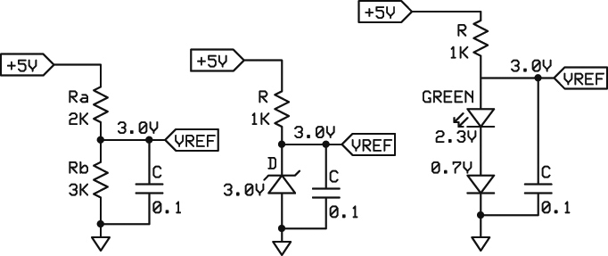
FIGURE 4. Supplying a reference voltage less than Vcc can be done in a number of ways. The best use diodes for better stability. Other methods are also possible.
The value returned by the A/D is the ratio of the input signal to the reference (or input divided by reference). So, if the reference is changed to three volts (instead of Vcc which is five volts), you will be able to use the full range of the A/D. You will need to check on the reference specifications of your particular A/D to see how low you can go. Ideally, you want the reference to equal the maximum input signal.
Note that generally A/D converters are tolerant of input voltages higher than the reference. They usually return a maximum value but are not damaged. However, virtually all A/Ds can be damaged by input voltages higher than Vcc. Using a lower reference voltage provides some safety margin should the input be larger than expected.
If your input is very small, you will need to add a gain circuit which multiplies the signal by some factor. Figure 5 shows a typical non-inverting op-amp gain stage.
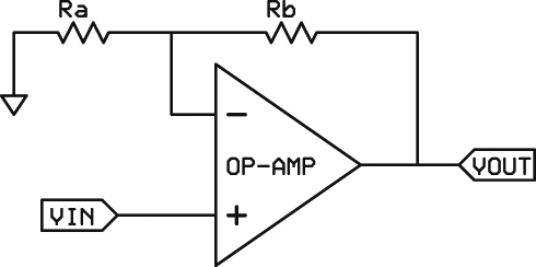
FIGURE 5. A typical non-inverting op-amp. The gain, or multiplication, is defined as: Vout = Vin * (Ra+Rb)/Ra.
The formula for finding the resistor ratios is: Vout = Vin (Ra+Rb)/Ra. High resistor ratios (megohms) can result in noise problems. Low resistor values (100s of ohms) will cause relatively high current consumption. Gain stages of 1,000 to 10,000 are reasonable if the frequencies are low. For higher frequencies, multiple stages will be required because the slew rate (a.k.a., gain bandwidth product) of a single amplifier will be exceeded.
Addition/Offset
Adding or subtracting a voltage from your sensor is not too difficult. Let’s assume your sensor produces an AC wave of ±2.5 volts and you want to see zero to five volts. Basically, you want to add 2.5 volts to the signal so that it will always be positive.
You can sort of do that with just resistors as shown in Figure 6. The result will be positive but not zero to five volts.
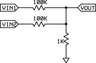
FIGURE 6. Voltage summing is simple. Just be sure that the resistor connected to ground is much less than the input resistors so that it will not limit the current. The input resistors do not have to be the same. If they are different, the voltages will sum proportionately. Note that the output is also divided by the resistor to ground.
Rsum collects all the currents coming from the other resistors and converts it to a voltage. Therefore, Rsum must be much lower than the other resistors so that it will not limit the current and give poor results. Typically, Rsum is about 1% of the other resistors. The second point is that the circuit acts as a voltage divider, as well as a summer. So as diagramed, the output will be about 1% of the input.
The input resistors do not have to be the same. If they are different, the lower-valued input resistor will have a proportionally larger effect on the sum. To determine any individual resistor ratio (see voltage dividers above to calculate the actual voltage), assume all the other input resistors are disconnected.
The incorrect output voltage can be fixed by adding a gain stage as shown in Figure 7.
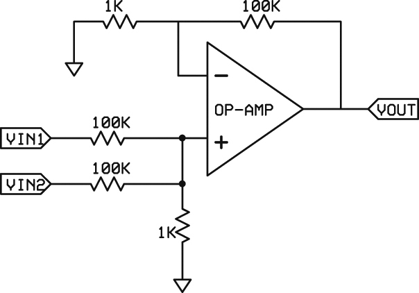
FIGURE 7. By adding a gain stage after the resistor summer, the output can be scaled properly. The op-amp gain setting resistors can be the same ratio as the summing resistors. Many other variations are possible.
The output is the algebraic sum of the two (or more) inputs. Conveniently, the resistor ratios for the feedback circuit are the same as the individual voltage dividers (in this case, 100:1). Different feedback resistor values can be used as long as the ratios are the same. As shown, the ±2.5V signal has been shifted by +2.5 volts so the output is zero to five volts.
You can, of course, use different feedback resistors and the output will be changed accordingly. This is seen as an overall scale factor change or: Vout = (Vin1 + Vin2) * gain. If you used different values for the input summing resistors, you will have to take that into consideration, as well. This is seen as a multiplication/division of an individual input according to the difference in the current supplied to the summing resistor. As you can see, very complicated relationships can be created.
Absolute Value/Rectification
Another way to eliminate the problem of negative input voltages is to simply remove them. The mathematical term rectification is generally associated with removing negative parts of a signal. This can be accomplished with a diode connected in series with the input signal. It’s a quick and dirty solution that also eliminates a positive portion of the signal, as well. Because of the forward voltage drop associated with diodes (typically 0.7 volts), the diode strips off 0.7 volts of the positive part of the signal, as well. This may or may not be a problem. (Losing the bottom 0.7 volts of a signal is equivalent to losing 3.5 bits of resolution in our eight-bit A/D.)
A precision rectifier (Figure 8) puts the diode in the feedback loop of an op-amp.
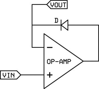
FIGURE 8. A simple precision half-wave rectifier puts the diode in the feedback loop. That eliminates the 0.7 volt forward voltage drop seen with a bare diode. The circuit will properly rectify millivolt signals (or less).
The result is that the 0.7 volt diode drop is eliminated. The whole positive part of the input signal is passed. You should include a negative supply for the op-amp because you should never apply an input signal that is below the negative rail. That being said, most op-amps have protective clamping diodes at the inputs to prevent damage and latch-up from negative voltages. So, if the current is kept very low (<< 1 mA) there is usually no problem for hobbyist-type applications. (Look at the datasheet to verify that there are protective diodes.)
Full-wave rectification is mathematically known as the absolute value of the input signal. You can get the absolute value of an AC signal by applying it to a full-wave rectifier. This is done all the time with power supplies. There is still the problem of the voltage drop associated with the diodes, though. Worse, the signal passes through two diodes, so the signal ±1.4 volts around ground is lost. A typical absolute value circuit is shown in Figure 9A. This eliminates the voltage drop problem associated with the diodes.
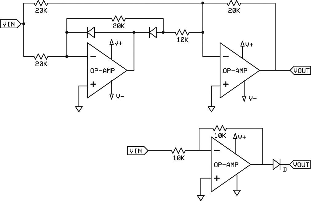
FIGURE 9A. A traditional absolute value circuit is shown on top. It requires a negative power supply. The lower circuit (FIGURE 9B) is much simpler and does not require a negative supply. However, it must be able to tolerate a negative voltage applied to the input.
Note that a negative power supply is required for this circuit.
Some op-amps — like the LMC6282 and family — are designed to allow a negative voltage to be applied to an input as long as it is current limited. This can be used to simplify the absolute value circuit and eliminate the need of a negative supply voltage.
Figure 9B shows this circuit. Note that the input signal and op-amp output are actually joined at the output. When the op-amp is outputting a positive half-cycle, it overwhelms the input portion. When the op-amp output is “off” (because of the reversed-biased diode), the input half-cycle signal passes through the two resistors to the output. This means that the half-cycles have different drive capabilities: high drive from the op-amp and low drive from the input (through the resistors). Therefore, this circuit must be connected to a high impedance load to maintain proper half-cycle amplitudes. Alternatively, it can be buffered with another op-amp.
Integration and Differentiation
Fundamentally, integration is usually not much more than applying the signal to a capacitor. Figure 10 shows a typical integrator.
FIGURE 10. An integrator is easy to implement. The switch is necessary to remove the charge on the capacitor (the resistor limits the discharge current). An electronic switch such as an FET can also be used.
The switch (which can certainly be electronic — like an FET) removes the charge on the capacitor before the integration function starts. Resistor R3 limits the current through the switch during capacitor discharge and is especially necessary for electronic switches. As shown, the output of the circuit will be the sum of the voltage applied to the input times the length of time applied, times 1/R1C. (R1 is the resistor value in ohms and C is the capacitor value in farads.) Use a quality capacitor with low leakage and low dielectric absorption. It is also important to keep R1 and R2 the same so that the bias currents are the same. Otherwise, the output can drift considerably, especially over temperature. The circuit works best with high input resistance op-amps (> teraohm). This circuit can also be characterized as a low pass filter with a corner frequency of 0 Hz.
There are a couple of points to ponder. If the input signal is removed or set to zero, the output voltage remains unchanged. This makes sense when you stop to think about it. Adding a lot of zeros to a sum doesn’t change the sum. In order to reduce the output, a negative voltage must be applied (and a negative power supply should be used for the op-amp, as well).
A reverse or inverted integrator can be created by applying the signal to the inverting input of the op-amp. In this way, a positive input signal will decrease the output. Note that the capacitor must be charged up for this to work, so the switch has to be changed (or better, a signal applied to the non-inverting input to charge the capacitor).
A differentiator is also fairly easy to implement in theory, as shown in Figure 11A.
FIGURE 11A. A theoretical differentiator uses only a resistor and capacitor. A more practical version (FIGURE 11B) uses an extra resistor and capacitor for stability.
However, there are problems. This circuit can be characterized as a high pass filter with the corner frequency at 0 Hz and a positive slope of 6 dB per octave. As such, noise can be a significant problem leading to instability (oscillation) and degraded performance. For that reason, an added RC network (R3, C2) is used to reduce the gain at high frequencies (see Figure 11B). The output of the circuit is the input times R1C1 times d/dt.
An inverted function can be obtained by applying the signal to the inverting input resistor and grounding the non-inverting input (as with the integrator above).
Proportional-Integral-Derivative Controller
Now that you know how to sum, multiply, integrate, and differentiate, you can combine them into a PID (Proportional Integral Derivative) controller. As you can see, it only takes a few parts to create a very sophisticated analog calculator. Analog PIDs can be very fast — as fast as the op-amps and settling times of the capacitors. Often, this is much faster than the µCs. Obviously, the big drawback with the analog system is that it can’t be changed easily. Plus, there is always the concern about component value drift,
especially over temperature. Nevertheless, analog PIDs have been around for decades and can be very effective.
X-Y Multiplication
Previously, we examined multiplication of a value by a constant but suppose you want to multiply two different values together. This is very different. We’ll look at a simple method that is easy to implement. There are more precise and complex circuits that can be built with op-amps, but it makes little sense to do so when you can buy a chip that does it all very cheaply. Analog multipliers/dividers are available for a few dollars. (For example, Analog Devices AD633 costs $7.75 at Jameco. Note that most commercial analog “multipliers” allow you to square and take the square root of a value, too.)
There are three things to mention. The first is about proper sign management. There are four possible combinations of signs (or quadrants) when combining two numbers: +X +Y, +X -Y, -X +Y, and -X -Y. The output should provide the proper sign. Not all circuits perform full “four quadrant” calculations. Often, this is not a circuit necessity. Most often — but not always — the magnitude of the result is correct. The second issue is that the terms multiplication and division often seem to be interchanged. This is because the division by a number greater than one can be represented by the multiplication of a number less than one. Figure 12 is an example of a “multiplier” circuit.
FIGURE 12. Two voltage dividers end up being called a multiplier because multiplying fractions can be the same as dividing by values greater than one.
From the point of view of two fractional numbers, this is true. However, the result is always smaller than the original values so the concept of division is also true. As shown, the output of Figure 12 is the fractional product of the two resistive dividers times the input voltage.
The last issue is that many circuits are not scaled for proper output. Their outputs are proportional to the function specified. Like the simple resistor summing circuit mentioned much earlier, the output is not the true sum of the inputs unless additional scaling operations are employed.
Multiplication
A simple way of multiplying two numbers is to create a variable gain amplifier. This can be accomplished by simply making the feedback resistor changeable. Figure 13A illustrates this.
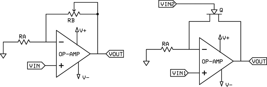
FIGURE 13A. Multiplication can be accomplished by changing the gain of the circuit with a variable resistor. FIGURE 13B does the same thing with an FET that changes its resistance according to the voltage applied to the gate.
The output is the input multiplied by the gain of the amplifier which is (RA+RB)/RA. If your sensor is a variable resistor of some type (like a thermistor), the circuit can be used as-is. If you have a voltage for VIN2, then you can use an FET instead (Figure 13B).
Note that the multiplication is not exactly linear because doubling RB does not exactly double the gain. There are many variations on this theme of gain changing for multiplication. Using a photocell instead of an FET is also practical. Important note: The leads to the variable resistor are inside the feedback loop of the op-amp and are extremely susceptible to noise and can easily cause op-amp oscillation. The leads must not be longer than a couple of inches.
Logs and Antilogs
Most higher function analog mathematics incorporate a log/antilog circuit. This allows you to multiply/divide and exponentiate easily. The procedure is to take the log of the value, perform simple addition/subtraction and/or multiplication/division, and then take the antilog. With this method, adding and subtracting is equivalent to multiplying and dividing. Multiplying and dividing becomes equivalent to raising to a power or extracting a root. So, taking the 3.5th root of a number can be accomplished by taking the log of the number, dividing by 3.5, and taking the antilog of that result.
There is a logarithmic relationship between the emitter base voltage of most silicon transistors. In theory, this allows a simple method to generate logs and antilogs. Figure 14A shows a simple log generator with the measured results. For every factor of 10 increase in the input, there is a “constant” increase of about 55 mV in the output. The error is about 10%. This is not great accuracy, but for feedback systems this may be perfectly adequate. Additionally, the circuit is quite temperature-sensitive, changing about 0.3% per degree C. (The capacitor helps to stabilize the op-amp and the diode protects the transistor from excessive reverse current from the op-amp. Neither is probably absolutely necessary.) Some of this error can be eliminated by a self-calibration routine in software.
The antilog circuit shown in Figure 14B should work but requires considerable effort.
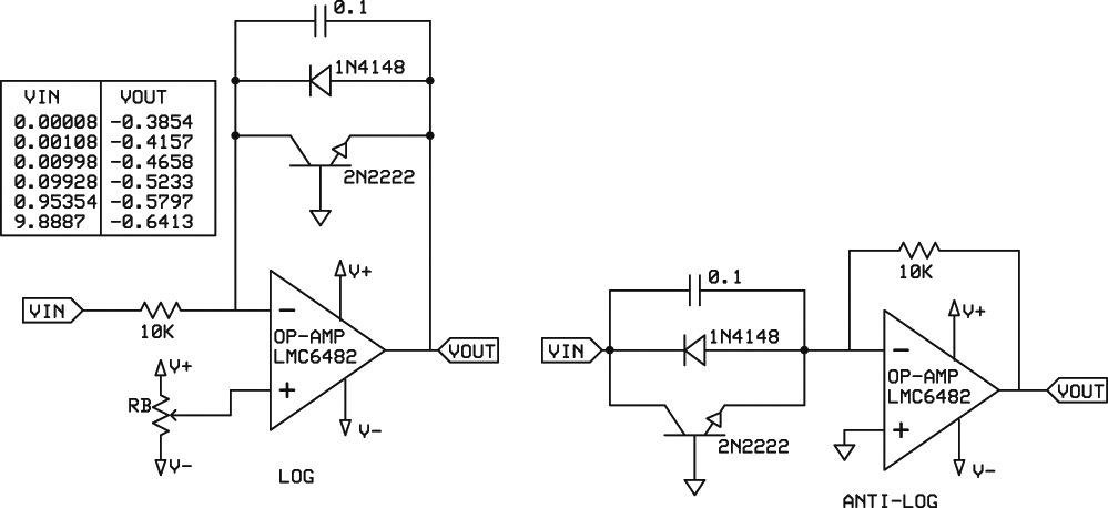
FIGURE 14A. The log circuit on the left is simple and works reasonably well. Actual measures are provided. The anti-log circuit (FIGURE 14B) provided poor results, although others have reported better performance.
It probably isn’t practical. However, it has been reported that with the proper matching of transistors, a log/antilog circuit (connecting Figures 14A and 14B in series) provided reasonable results.
More complex and much more accurate log/antilog circuits can be constructed. Typically, these consist of a couple of op-amps, a half dozen resistors, two transistors, and a special temperature-compensating resistor. The accuracy of these circuits can be very good — about 1% over six to seven decades of operation. However, in practice, these are probably too complex for typical mC applications. (See References for further reading.)
The charging of a capacitor through a resistor also follows a exponential relationship (power of two rather than a power of 10). For every one time constant, the capacitor voltage moves about 63% from where it is towards the supply voltage. I am not aware of any circuit that uses this characteristic for mathematical operation, however it could be useful. (Apply a voltage for a fixed time to a resistor/capacitor network and measure the voltage through the µC’s A/D.)
Conclusion
Analog mathematics can be added to your microcontroller system to streamline your design and make it more efficient. Whether it’s simple scaling or complicated functions, there are many basic circuits that can assist in calculations. This removes some of the burden from your code and can speed up your whole system. (Note that all circuits were built and tested using an National Semiconductor LMC6484 op-amp.) NV
References
National Semiconductor Application Notes: AN-4, AN-20, AN-30 (log converters), AN31, LMC6482 datasheet.
Signetics: “Operational Amplifiers.”
Analog Devices: Analog Multipliers/Dividers (various datasheets).
Forrest Mims: January 1979, February 1979, Popular Electronics.