The bipolar transistor is the most important “active” circuit element used in modern electronics, and it forms the basis of most linear and digital ICs and op-amps, etc. In its discrete form, it can function as either a digital switch or as a linear amplifier, and is available in many low, medium, and high power forms. This opening episode concentrates on basic transistor theory, characteristics, and circuit configurations. The remaining seven parts of the series will present a wide range of practical bipolar transistor application circuits.
BIPOLAR TRANSISTOR BASICS
A bipolar transistor (first invented in 1948) is a three-terminal (base, emitter, and collector), current-amplifying device in which a small input current can control the magnitude of a much larger output current. The term “bipolar” means that the device is made from semiconductor materials in which conduction relies on both positive and negative (majority and minority) charge carriers.
A normal transistor is made from a three-layer sandwich of n-type and p-type semiconductor material, with the base or “control” terminal connected to the central layer, and the collector and emitter terminals connected to the outer layers. If it uses an n-p-n construction sandwich, as in Figure 1(a), it is known as an npn transistor and uses the standard symbol in Figure 1(b).
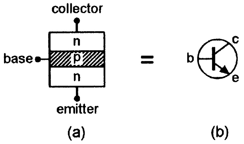
FIGURE 1. Basic construction (a) and symbol (b) of npn transistor.
If it uses a p-n-p structure, as in Figure 2(a), it is known as a pnp transistor and uses the symbol in Figure 2(b).
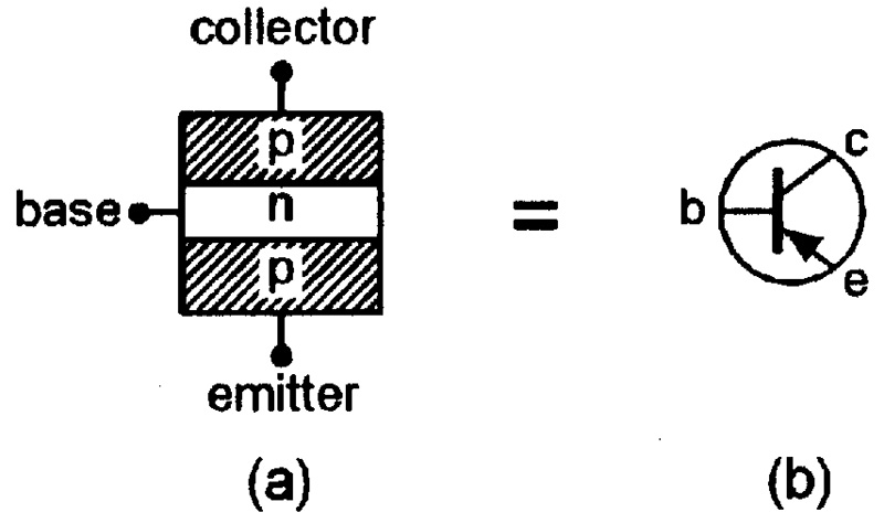
FIGURE 2. Basic construction (a) and symbol (b) of pnp transistor.
In use, npn and pnp transistors each need a power supply of the appropriate polarity, as shown in Figure 3.
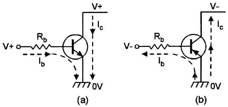
FIGURE 3. Polarity connections to (a) npn and (b) pnp transistors.
An npn device needs a supply that makes the collector positive to the emitter — its output or main-terminal signal current (Ic) flows from collector to emitter, and its amplitude is controlled by an input “control” current (Ib) that flows from base to emitter via an external current-limiting resistor (Rb) and a positive bias voltage. A pnp transistor needs a negative supply — its main terminal current flows from emitter to collector, and is controlled by an emitter-to-base input current that flows to a negative bias voltage.
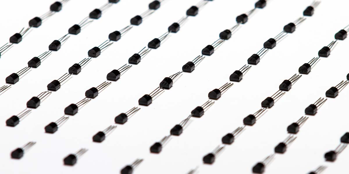
In the early years of bipolar transistor usage, most transistors were made from germanium semiconductor materials. Such devices had many practical disadvantages: they were fragile, excessively temperature-sensitive, electronically noisy, and had very poor power-handling capacities. Germanium transistors are now obsolete. Virtually all modern bipolar transistors are made from silicon semiconductor materials. Such devices are robust, have good power-handling capacities, are not excessively temperature sensitive, and generate negligible electronic noise.
Today, a very wide variety of excellent silicon bipolar transistor types are readily available. Figure 4 lists the basic characteristics of two typical general-purpose, low-power types — the 2N3904 (npn) and the 2N3906 (pnp) — which are each housed in a TO-92 plastic case and have the under-side pin connections shown in the diagram.
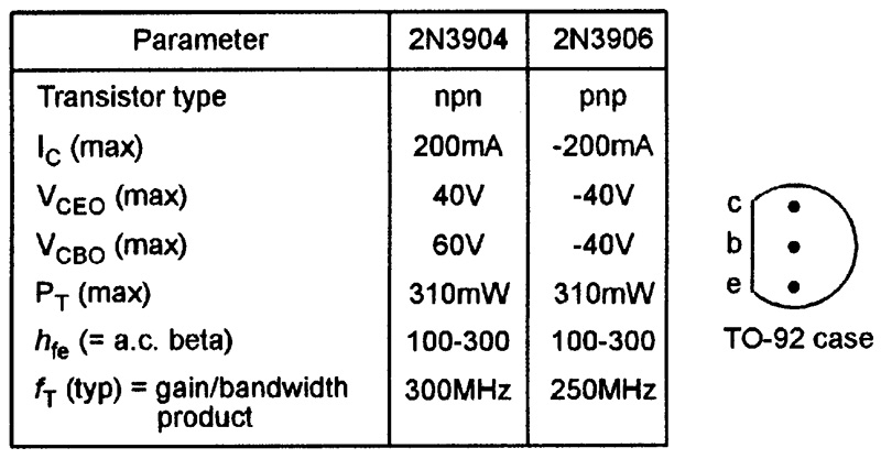
FIGURE 4. General characteristics and outlines of the 2N3904 and 2N3906 low-power silicon transistors.
Note, when reading the Figure 4 list, that VCEO(max) is the maximum voltage that may be applied between the collector and emitter when the base is open-circuit, and VCBO(max) is the maximum voltage that may be applied between the collector and base when the emitter is open-circuit. IC(max) is the maximum mean current that can be allowed to flow through the collector terminal of the device, and PT(max) is the maximum mean power that the device can dissipate, without the use of an external heatsink, at normal room temperature.
One of the most important parameters of the transistor is its forward current transfer ratio, or hfe — this is the current-gain or output/input current ratio of the device (typically 100 to 300 in the two devices listed). Finally, the fT figure indicates the available gain/bandwidth product frequency of the device, i.e., if the transistor is used in a voltage feedback configuration that provides a voltage gain of x100, the bandwidth is 1/100 of the fT figure, but if the voltage gain is reduced to x10, the bandwidth increases to fT/10, etc.
TRANSISTOR CHARACTERISTICS
To get the maximum value from a transistor, the user must understand both its static (DC) and dynamic (AC) characteristics. Figure 5 shows the static equivalent circuits of npn and pnp transistors.
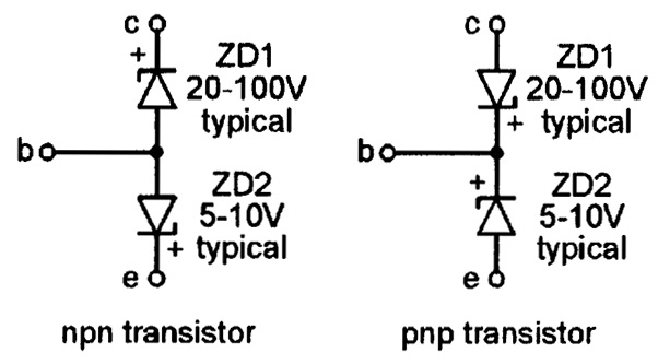
FIGURE 5. Static equivalent circuits of npn and pnp transistors.
A zener diode is inevitably formed by each of the transistor’s n-p or p-n junctions, and the transistor is thus (in static terms) equal to a pair of reverse-connected zener diodes wired between the collector and emitter terminals, with the base terminal wired to their “common” point. In most low-power, general-purpose transistors, the base-to-emitter junction has a typical zener value in the range 5V to 10V — the base-to-collector junction’s typical zener value is in the range 20V to 100V.
Thus, the transistor’s base-emitter junction acts like an ordinary diode when forward-biased and as a zener when reverse-biased. In silicon transistors, a forward-biased junction passes little current until the bias voltage rises to about 600mV, but beyond this value, the current increases rapidly. When forward-biased by a fixed current, the junction’s forward voltage has a thermal coefficient of about -2mV/0C. When the transistor is used with the emitter open-circuit, the base-to-collector junction acts like that just described, but has a greater zener value. If the transistor is used with its base open-circuit, the collector-to-emitter path acts like a zener diode wired in series with an ordinary diode.
The transistor’s dynamic characteristics can be understood with the aid of Figure 6, which shows the typical forward transfer characteristics of a low-power npn silicon transistor with a nominal hfe (current gain) value of 100.
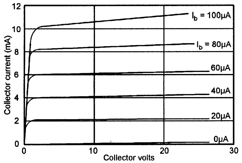
FIGURE 6. Typical transfer characteristics of low-power npn transistors with hfe value of 100 nominal.
Thus, when the base current (Ib) is zero, the transistor passes only a slight leakage current. When the collector voltage is greater than a few hundred millivolts, the collector current is almost directly proportional to the base currents, and is little influenced by the collector voltage value. The device can thus be used as a constant-current generator by feeding a fixed bias current into the base, or can be used as a linear amplifier by superimposing the input signal on a nominal input current.
PRACTICAL APPLICATIONS
A transistor can be used in a variety of different basic circuit configurations, and the remainder of this opening episode presents a brief summary of the most important of these. Note that although all circuits are shown using npn transistor types, they can be used with pnp types by simply changing circuit polarities, etc.
DIODE AND SWITCHING CIRCUITS
The base-emitter or base-collector junction of a silicon transistor can be used as a simple diode or rectifier, or as a zener diode by using it in the appropriate polarity. Figure 7 shows two alternative ways of using an npn transistor as a simple diode clamp that converts an AC-coupled rectangular input waveform into a rectangular output that swings between zero and a positive voltage value, i.e., which “clamps” the output signal to the zero-volts reference point via either the transistor’s internal base-emitter or base-collector “diode” junction.
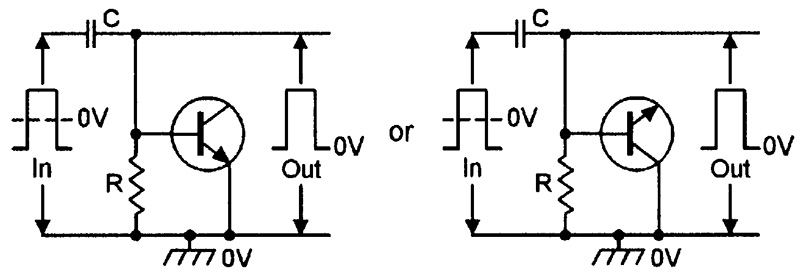
FIGURE 7. Clamping diode circuit, using an npn transistor as a diode.
Figure 8 shows an npn transistor used as a zener diode that converts an unregulated supply voltage into a fixed-value regulated output with a typical value in the range 5V to 10V, depending on the individual transistor. Only the reverse-biased base-emitter junction of the transistor is suitable for use in this application. If the reverse-biased base-collector junction is used, the zener value typically rises into the 30V-100V range, and the transistor may self-destruct (due to over-heating) at fairly low zener current levels.
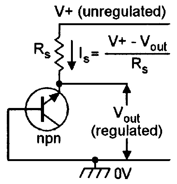
FIGURE 8. A transistor used as a zener diode.
Figure 9 shows a transistor used as a simple electronic switch or digital inverter. Its base is driven (via Rb) by a digital input that is at either zero volts or at a positive value, and load RL is connected between the collector and the positive supply rail. When the input voltage is zero, the transistor is cut off and zero current flows through the load, so the full supply voltage appears between the collector and emitter. When the input is high, the transistor switch is driven fully on (saturated) and maximum current flows in the load, and only a few hundred millivolts are developed between the collector and emitter. The output voltage is thus an inverted form of the input signal.
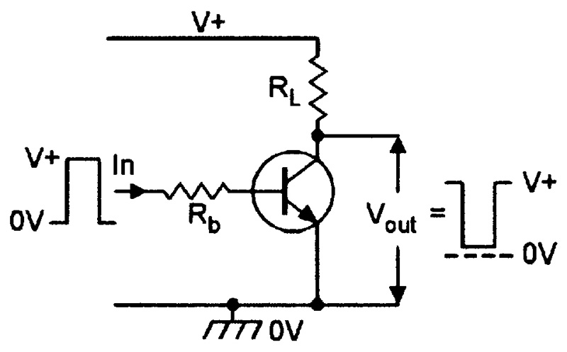
FIGURE 9. Transistor switch or digital inverter.
The basic Figure 9 circuit is intended for use as a simple digital switch or inverter, driving a purely resistive load. It can be used as an electronic switch that drives a relay coil or other highly inductive load (such as a DC motor) by connecting it as shown in Figure 10, in which diodes D1 and D2 protect the transistor from high-value switch-off-induced back EMFs from the inductive load at the moment of power switch-off.
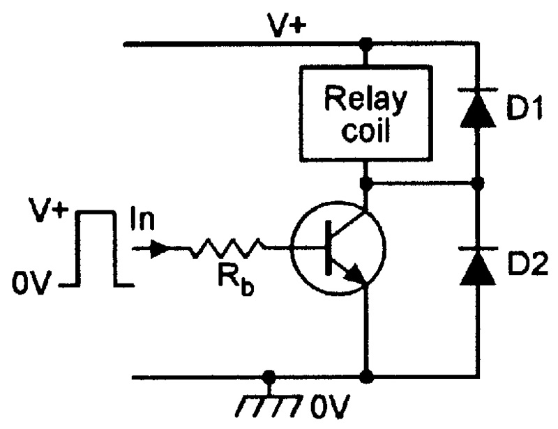
FIGURE 10. Transistor switch (digital inverter) driving a relay coil (or other inductive load).
LINEAR AMPLIFIER CIRCUITS
A transistor can be used as a linear current or voltage amplifier by feeding a suitable bias current into its base and then applying the input signal between an appropriate pair of terminals. The transistor can, in this case, be used in any one of three basic operating modes, each of which provides a unique set of characteristics. These three modes are known as “common-emitter” (Figure 11), “common-base” (Figure 12), and “common-collector” (Figures 13 and 14).
In the common-emitter circuit (which is shown in very basic form in Figure 11), resistive load RL is wired between the transistor’s collector and the positive supply line, and a bias current is fed into the base via resistor Rb, whose value is chosen to set the collector at a quiescent half-supply voltage value (to provide maximum undistorted output signal swings). The input signal is applied between the transistor’s base and emitter via capacitor C, and the output signal (which is phase-inverted relative to the input) is taken between the collector and emitter. This circuit gives a medium-value input impedance and a fairly high overall voltage gain.
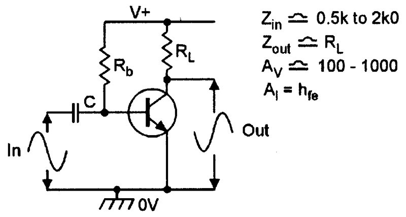
FIGURE 11. Common-emitter linear amplifier.
In the common-base circuit in Figure 12, the base is biased via Rb and is AC-decoupled (or AC-grounded) via capacitor Cb. The input signal is effectively applied between the emitter and base via C1, and the amplified but non-inverted output signal is effectively taken from between the collector and base. This circuit features good voltage gain, near-unity current gain, and a very low input impedance.
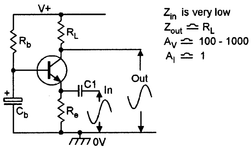
FIGURE 12. Common-base linear amplifier.
In the DC common-collector circuit in Figure 13, the collector is shorted to the low-impedance positive supply rail and is thus effectively at “virtual ground” impedance level. The input signal is applied between base and ground (virtual collector), and the non-inverted output is taken from between emitter and ground (virtual collector). This circuit gives near-unity overall voltage gain, and its output “follows” the input signal. It is thus known as a DC-voltage follower (or emitter follower) and it has a very high-input impedance (equal to the product of the RL and hfe values).
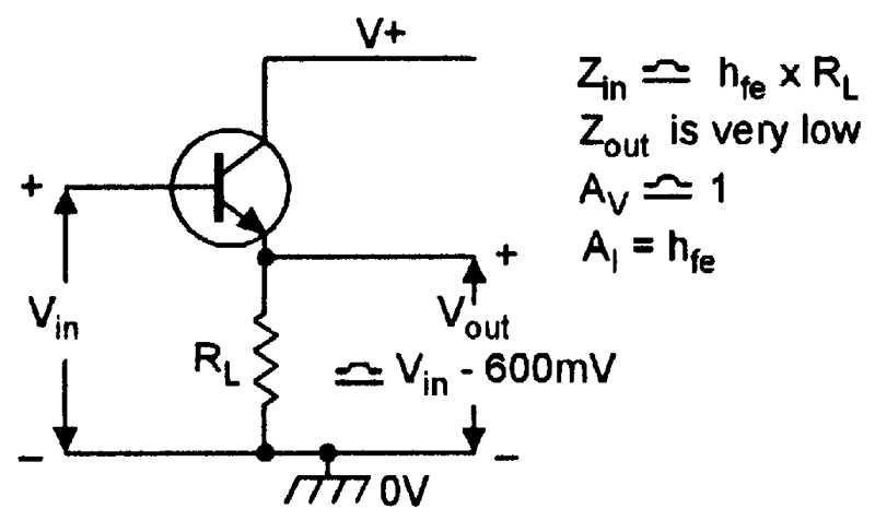
FIGURE 13. DC common-collector linear amplifier or voltage follower.
Note that the above circuit can be modified for AC use by simply biasing the transistor to half-supply volts and AC-coupling the input signal to the base, as shown in the basic circuit in Figure 14, in which potential divider R1-R2 provides the half-supply-voltage biasing.
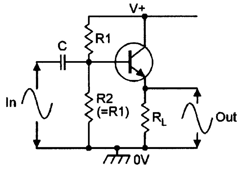
FIGURE 14. AC common-collector amplifier or voltage follower.
The chart in Figure 15 summarizes the performances of the three basic amplifier configurations. Thus, the common-collector amplifier gives near-unity overall voltage gain and a high input impedance, while the common-emitter and common-base amplifiers both give high values of voltage gain, but have medium to low values of input impedance.
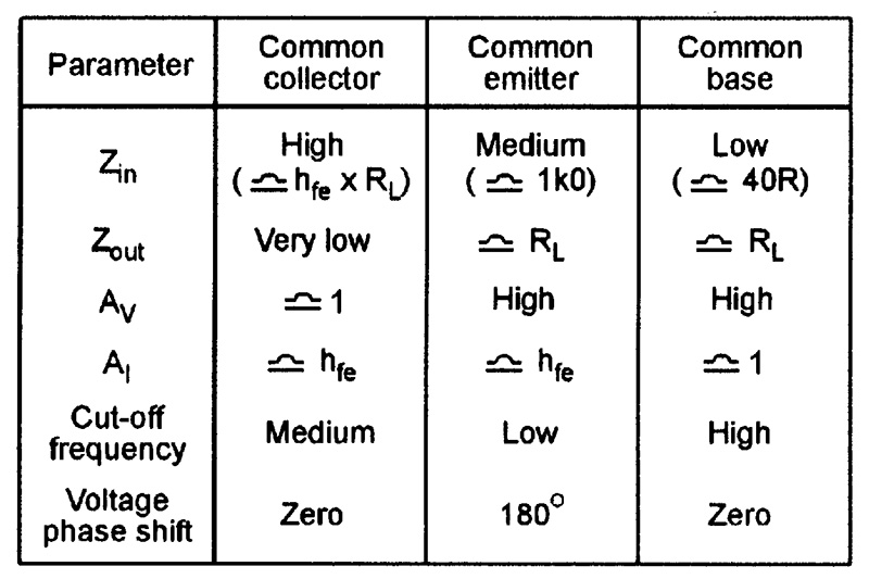
FIGURE 15. Comparative performances of the three basic circuit configurations.
THE DIFFERENTIAL AMPLIFIER
Figure 16 shows — in basic form — how a pair of amplifiers of the basic Figure 11 type can be coupled together to make a “differential” amplifier or “long-tailed pair” that produces an output signal that is proportional to the difference between the two input signals. In this case, Q1 and Q2 share a common emitter resistor (the “tail”), and the circuit is biased (via R1-R2 and R3-R4) so that the two transistors pass identical collector currents (thus giving zero difference between the two collector voltages) under quiescent zero-input conditions.
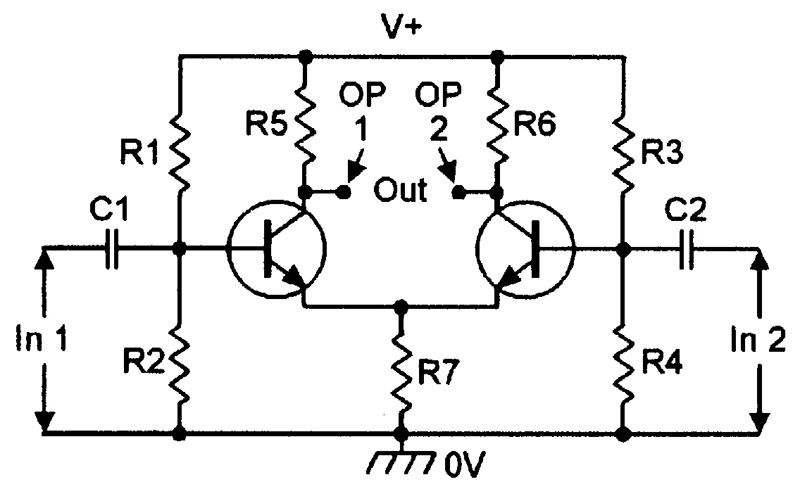
FIGURE 16. Differential amplifier or long-tailed pair.
If, in the above circuit, a rising input voltage is applied to the input of one transistor only, it makes the output voltage of that transistor fall and (as a result of emitter-coupling action) makes the output voltage of the other transistor rise by a similar amount, thus giving a large differential output voltage between the two collectors. If identical signals are applied to the inputs of both transistors, on the other hand, both collectors will move by identical amounts, and the circuit will thus produce a zero differential output signal. The circuit therefore produces an output signal that is proportional to the difference between the two input signals.
THE DARLINGTON CONNECTION
The input impedance of the Figure 13 emitter follower circuit equals the product of RL and the transistor’s hfe values — if an ultra-high input impedance is wanted, it can be obtained by replacing the single transistor with a pair of transistors connected in the “Darlington” or Super-Alpha configuration, as shown in Figure 17. Here, the emitter current of the input transistor feeds directly into the base of the output transistor, and the pair act like a single transistor with an overall hfe value equal to the product of the two individual hfe values, i.e., if each transistor has an hfe value of 100, the pair act like a single transistor with an hfe of 10,000, and the overall circuit presents an input impedance of 10,000 x RL.
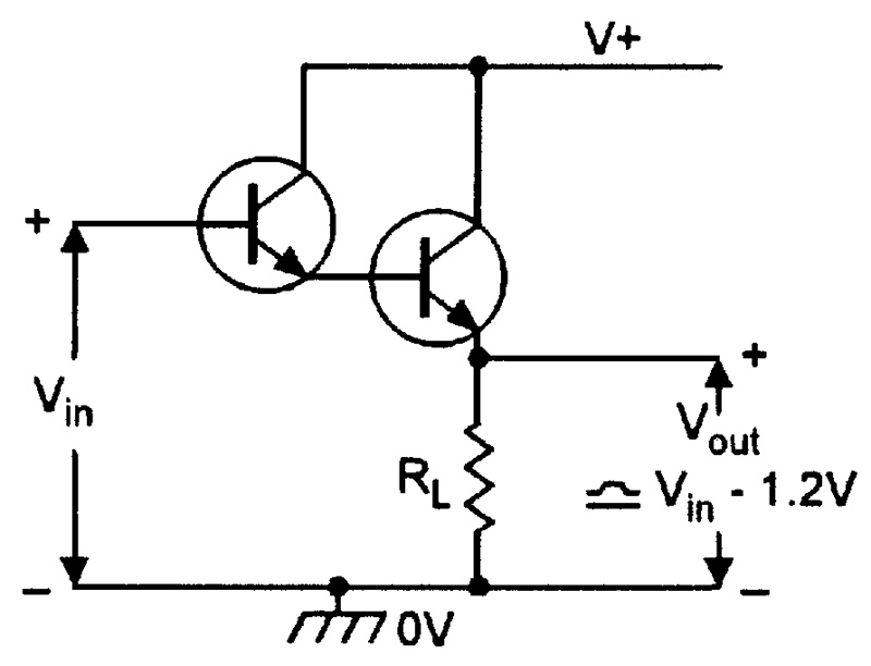
FIGURE 17. Darlington or Super-Alpha DC emitter follower.
MULTIVIBRATOR CIRCUITS
A multivibrator is, in essence, a two-state digital circuit that can be switched from the output-high to the output-low state, or vice versa, via a trigger signal that may be derived from an external source or via an automatic or triggered timing mechanism. Transistors can be used in four basic types of multivibrator circuits, as shown in Figures 18 to 21.
The Figure 18 circuit is a simple, manually-triggered, cross-coupled bistable multivibrator, in which the base bias of each transistor is derived from the collector of the other, so that one transistor automatically turns off when the other turns on, and vice versa.
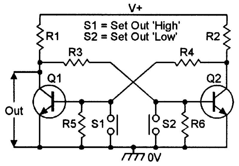
FIGURE 18. Manually-triggered bistable multivibrator.
Thus, the output can be driven low by briefly turning Q2 off via S2, thus shorting Q2’s base-emitter path. As Q2 turns off R2-R4 feed base drive to Q1 base, the circuit automatically locks into this state until Q1 is similarly turned off via S1, at which point the output locks into the high state again, and so on ad infinitum.
Figure 19 shows — in basic form — a monostable multivibrator or one-shot pulse generator circuit. Its output (from Q1 collector) is normally low, since Q1 is normally biased on via R5, but switches high for a preset period (determined by the C1-R5 component values) if Q1 is briefly turned off by momentarily closing push-button “Start” switch S1.
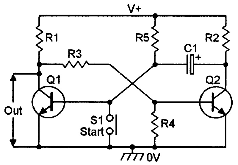
FIGURE 19. Manually-triggered monostable multivibrator.
The actual monostable timing period starts as the push-button “Start” switch is released, and has a period (P) of approximately 0.7 x C1 x R5, where P is in µS, C is in µF, and R is in kilohms.
Figure 20 shows an astable multivibrator, or free-running squarewave generator, in which the on and off periods of the squarewave are determined by the C1-R4 and C2-R3 component values. Basically, this circuit acts like a pair of cross-coupled monostable circuits, which automatically trigger each other sequentially. If the C1-R4 and C2-R3 timing periods are identical, the circuit generates a free-running squarewave output waveform. If the two timing periods are not identical, the circuit generates an asymmetrical output waveform.
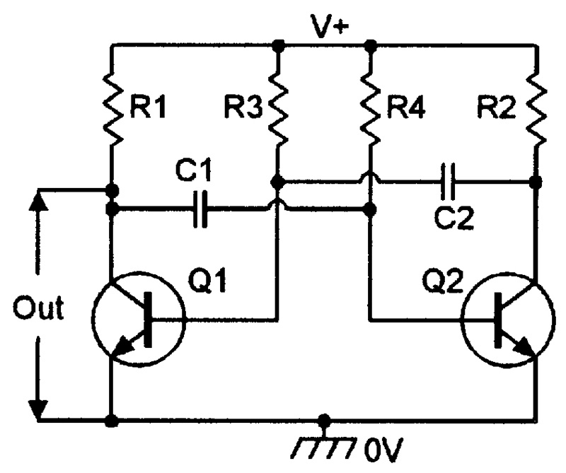
FIGURE 20. Astable multivibrator or free-running squarewave generator.
Finally, Figure 21 shows a basic Schmitt trigger or sine-to-square waveform converter circuit. The circuit action here is such that Q2 switches abruptly from the “on” state to the “off” state, or vice versa, as Q1 base goes above or below pre-determined “trigger” voltage levels.
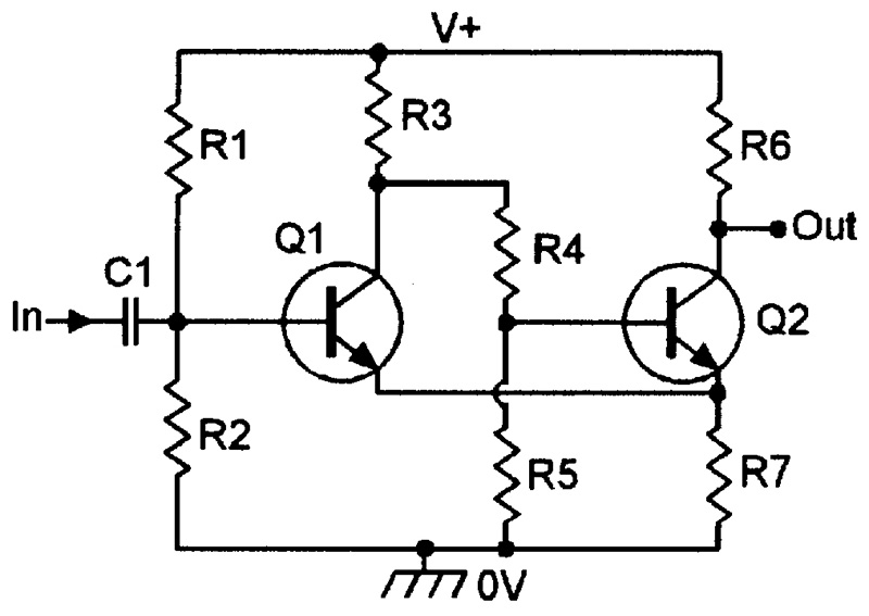
FIGURE 21. Schmitt trigger or sine-to-square waveform converter.
If the circuit’s input is fed with a reasonable-amplitude sinewave input, the circuit thus generates a sympathetic squarewave output waveform. NV