The two most widely used types of transistor waveform generator circuits are the oscillator types that produce sine waves and use transistors as linear amplifying elements, and the multivibrator types that generate square or rectangular waveforms and use transistors as digital switching elements.
Our last installment covered practical circuits of the oscillator type. This time, we describe ways of using bipolars to make practical multivibrator types of waveform generator circuits.
MULTIVIBRATOR CIRCUIT TYPES
Multivibrators are two-state (output high or output low) circuits that can be switched between one state and the other via a suitable trigger signal, which may be generated either internally or externally. There are four basic types of multivibrator (multi) circuits, and they are all useful in waveform generating applications. Of these four, the astable has two quasi-stable states and is useful as a free-running square wave generator. The monostable has one stable and one quasi-stable state and is useful as a triggered pulse generator. The bistable has two stable states and is useful as a triggered stop/go or high/low waveform generator. Lastly, the Schmitt has two stable input-voltage-sensitive states and is useful as a sine-to-square waveform converter or threshold switch.
ASTABLE MULTIVIBRATOR BASICS
Figure 1 shows the circuit and generated waveforms of a simple 1 kHz astable multivibrator, in which the two transistors are cross-coupled (from collector to base) via timer networks C1-R1 and C2-R2. The basic circuit action is such that, at the moment that power is initially switched to the circuit, inevitable differences in the precise characteristics of Q1 and Q2 make one transistor turn on slightly faster than the other, and the cross-coupling then causes a regenerative switching action to take place in which one transistor switches abruptly on and the other switches abruptly off.
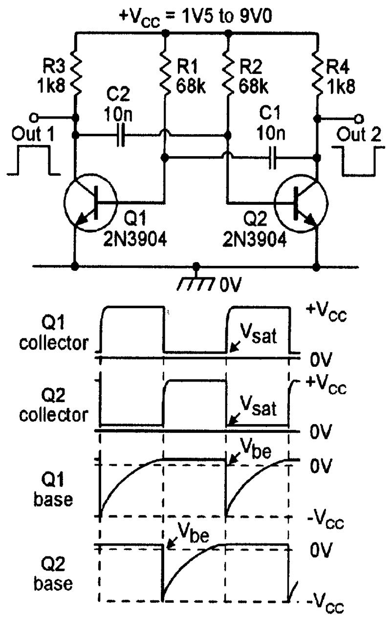
FIGURE 1. Circuit and waveforms of a basic 1 kHz astable multivibrator.
After a delay determined by the C1-R1 or C2-R2 time constant, the off transistor starts to turn on again, and the cross-coupling then causes another regenerative action in which the two transistors abruptly change state again. The whole process then repeats add infinitum. Thus, the basic Figure 1 circuit acts as a self-oscillating regenerative switch in which the on and off periods are controlled by the C1-R1 and C2-R2 time constants. If these time constants are equal (C1=C2=C, and R1=R2=R), the circuit acts as a square wave generator and operates at a frequency of about 1/(1.4CR). The frequency can be decreased by raising the C or R values, or increased by reducing the C or R values, or can be made variable by using twin-gang variable resistors (in series with 10K limiting resistors) in place of R1 and R2.
Outputs can be taken from either collector, and the two outputs are in anti-phase. The Figure 1 circuit’s operating frequency is almost independent of supply-rail values in the range 1.5 V to 9.0 V; the upper voltage limit is set by the fact that, as the transistors change state at the end of each half-cycle, the base-emitter junction of the off one is reverse biased by an amount almost equal to the supply voltage and will zener (and upset the timing action) if this voltage exceeds the junction’s reverse breakdown voltage value (which is typically about 10 V).
This problem can be overcome by wiring a silicon diode in series with the input of each transistor, to raise its effective zener value to that of the diode, as shown in Figure 2.
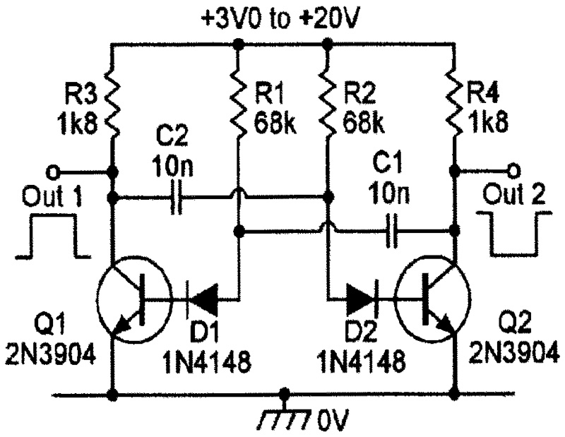
FIGURE 2. Wide-supply-voltage example of a 1 kHz astable multivibrator.
This protected circuit can be used with any supply in the range 3 V to 20 V, and gives a frequency variation of only 2% when the supply is varied from 6 V to 18 V. This variation can be reduced to a mere 0.5% by wiring an additional compensation diode in series with the collector of each transistor, as shown in the circuit of Figure 3.
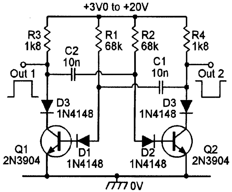
FIGURE 3. High-stability version of the basic Figure 2 1 kHz astable multivibrator circuit.
ASTABLE CIRCUIT VARIATIONS
The basic Figure 1 astable circuit can be usefully modified in several ways, either to improve its performance or to alter the type of output waveform that it generates. Some of the most popular of these variations are shown in Figures 4 through 9.
One weakness of the basic Figure 1 circuit is that the leading edges of its output waveforms are slightly rounded — the larger the values of timing resistors R1-R2 relative to collector load resistors R3-R4, the squarer the edges become. The maximum usable R1-R2 values are, in fact, limited to hfe x R3 (or R4), and one obvious way of improving the waveforms is to replace Q1 and Q2 with Darlington connected pairs of transistors and then use very large R1 and R2 values, as in the Figure 4 circuit, in which R1 and R2 can have values up to 12M, and the circuit can use any supply from 3 V to 18 V.
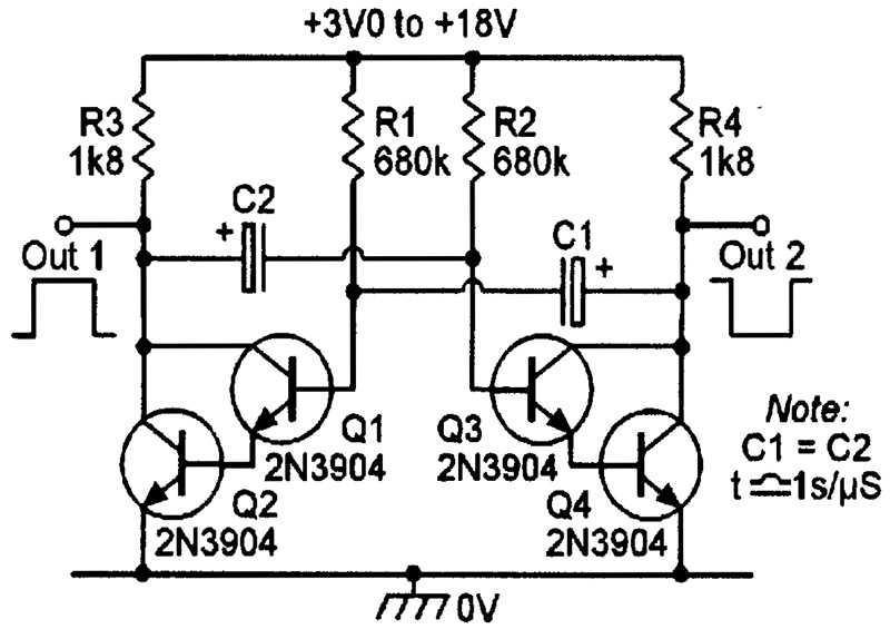
FIGURE 4. Long-period astable multivibrator.
With the R1-R2 values shown, the circuit gives a total period or cycling time of about one second per µF when C1 and C2 have equal values, and gives an excellent square wave output. The leading-edge rounding of the Figure 1 circuit can be eliminated by using the modifications of Figure 5, in which steering or waveform-correction diodes D1 and D2 automatically disconnect their respective timing capacitors from the transistor collectors at the moment of transistor switching. The circuit’s main time constants are set by C1-R1 and C2-R2, but the effective collector loads of Q1 and Q2 are equal to the parallel resistances of R3-R4 or R5-R6.
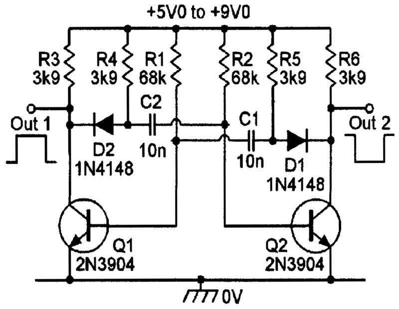
FIGURE 5. 1 kHz astable with waveform correction via steering diodes D1 and D2.
A minor weakness of the basic Figure 1 circuit is that if its supply is slowly raised from zero to its normal value, both transistors may turn on simultaneously, and the oscillator will not start. This snag can be overcome by using the sure-start circuit of Figure 6, in which the timing resistors are connected to the transistor collectors in such a way that only one transistor can be on at a time.
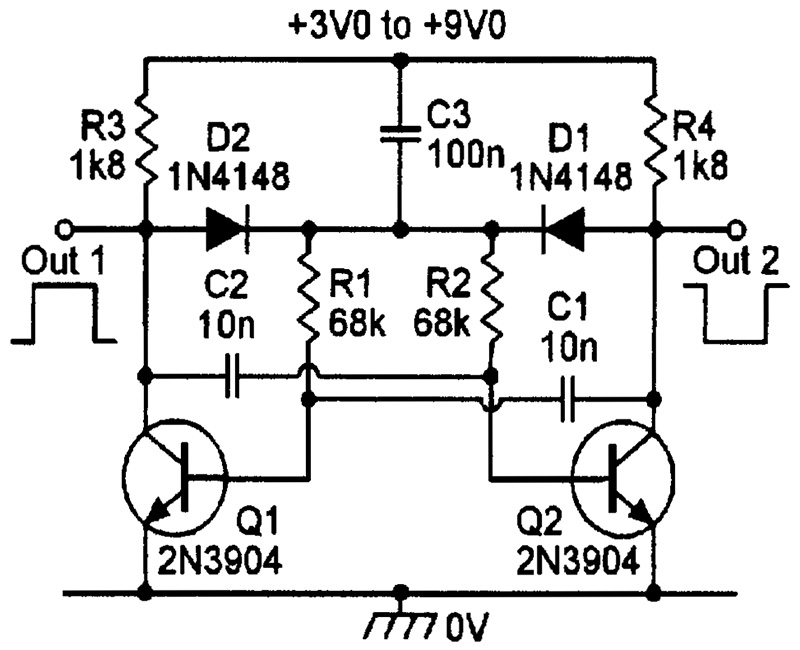
FIGURE 6. 1 kHz astable with sure-start facility.
All astable circuits shown so far give symmetrical output waveforms, with a 1:1 mark/space ratio. A non-symmetrical waveform can be obtained by making one set of astable time constants larger than the other. Figure 7 shows a fixed-frequency (1,100 Hz) generator in which the mark/space ratio is variable from 1:10 to 10:1 via RV1.
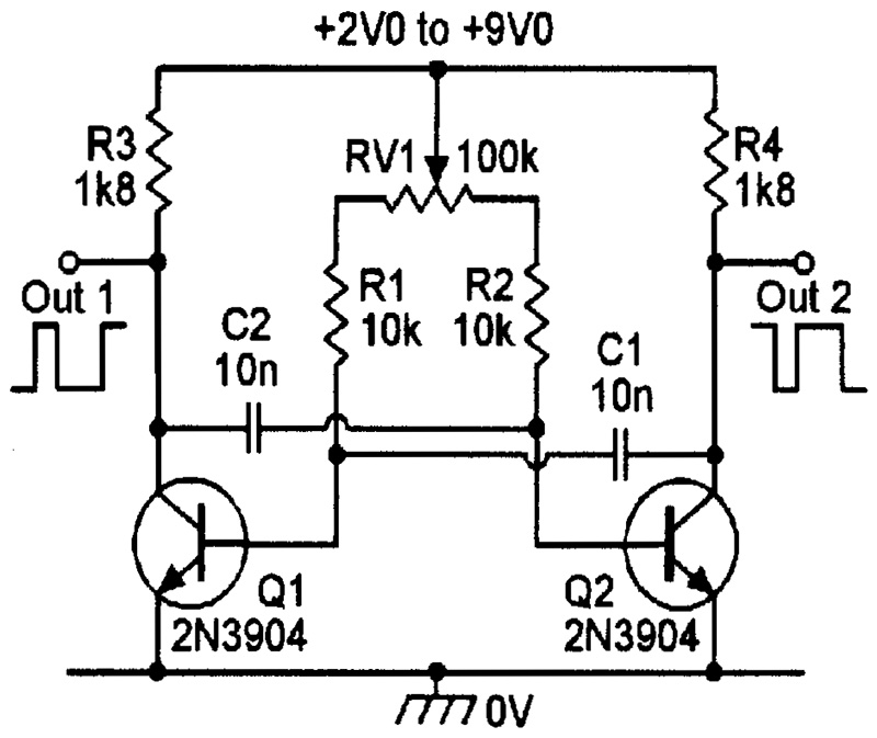
FIGURE 7. Basic 1,100 Hz variable mark/space ratio generator.
The leading edges of the output waveforms of the above circuit may be objectionably rounded when the mark-space control is set to its extreme positions. Also, the circuit may not start if its supply is applied too slowly. Both of these snags are overcome in the circuit of Figure 8, which is fitted with both sure-start and waveform-correction diodes.
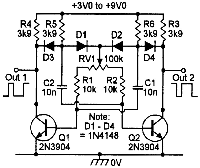
FIGURE 8. 1,100 Hz variable mark/space ratio generator with waveform correction and sure-start facility.
Finally, Figure 9 shows a basic astable circuit modified so that its frequency is variable over a 2:1 range (from 20 kHz down to 10 kHz) via a single pot, and so that its generated waveform can be frequency modulated via an external low-frequency signal. Timing resistors R3 and R4 have their top ends taken to RV1 pot and the frequency is greatest when the pot is at the positive supply line. Frequency modulation is obtained by feeding the low-frequency signal to the tops of R3-R4 via C4; C3 presents a low impedance to the carrier signal, but a high impedance to the modulating one.
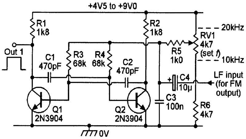
FIGURE 9. Astable with variable-frequency and FM facility.
MONOSTABLE BASICS
Monostable multivibrators are pulse generators, and may be triggered either electronically or manually. Figure 10 shows a circuit of the latter type, which is triggered by feeding a positive pulse to Q2 base via S1 and R6. This circuit operates as follows. Normally, Q1 is driven to saturation via R5, so the output (Q1 collector) is low. Q2 (which derives its base-bias from Q1 collector via R3) is cut off under this condition, so C1 is fully charged. When a start signal is applied to Q2 base via S1, Q2 is driven on and its collector goes low, reverse biasing Q1 base via C1 and thus initiating a regenerative switching action in which Q1 is turned off (and its output switches high) via C1’s negative charge, and Q2 is driven on via R1-R3 after S1 is released. As soon as the switching is complete, C1 starts to discharge via R5, until its charge falls to such a low value that Q1 starts to turn on again, thus initiating another regenerative action in which the transistors revert to their original states and the output pulse terminates, completing the action.
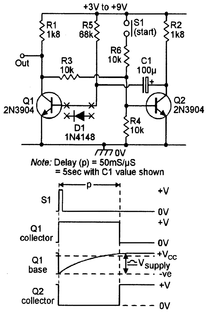
FIGURE 10. Basic manually-triggered monostable pulse generator.
Thus, a positive pulse is developed at the Q1 output each time an input trigger signal is applied via S1. The pulse period (P) is determined by the R5-C1 values, and approximates 0.7 x R5 x C1, where P is in mS, C is in µF, and R is in kilohms, and equals about 50mS/µF in the example shown. In practice, the Figure 10 circuit can be triggered either by applying a negative pulse to Q1 base or a positive one to Q2 base (as shown). Note that the base-emitter junction of Q1 is reverse biased by a peak amount equal to VSUPPLY during the operating cycle, thus limiting the maximum usable supply voltage to about 9 V. Greater supply voltages can be used by wiring a silicon diode in series with Q1 base, as shown by D1 in the diagram, to give the same frequency correction action as described earlier for the astable circuit.
LONG DELAYS
The value of timing resistor R5 must be large relative to R2, but must be less than the product of R1 and Q1’s hfe value. Very long timing periods can be obtained by using a Darlington or Super-Alpha pair of transistors in place of Q1, thus enabling large R5 values to be used, as shown in the Figure 11 circuit, which gives a pulse period of about 100 seconds with the component values shown.
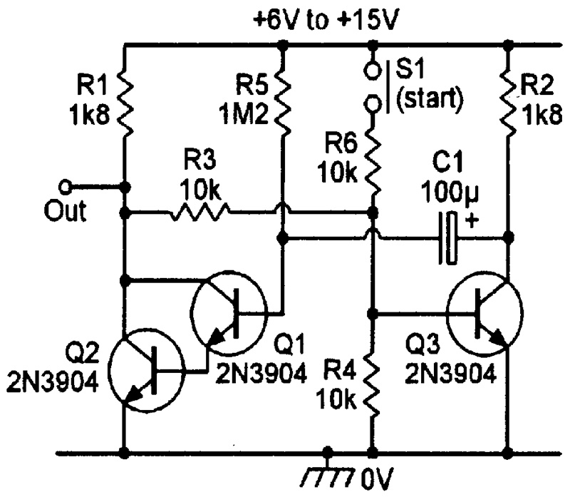
FIGURE 11. Long-period (100 second) monostable circuit.
An important point to note is that the basic Figure 10 circuit actually triggers at the moment of application (via S1 and R6) of a positive-going pulse to the base of Q2. If this pulse is removed before the monostable completes its natural timing period, the pulse will end regeneratively in the way already described, but if the trigger pulse is not removed (via S1) at this time, the monostable period will end non-regeneratively and will have a longer period and fall-time than normal. This problem can be eliminated by using electronic (rather than manual) triggering, as described in the next section.
ELECTRONIC TRIGGERING
Figures 12 and 13 show alternative ways of applying electronic triggering to the monostable pulse generator. In each case, the circuit is triggered by a square wave input with a short rise time. This waveform is differentiated by C2-R6, to produce a brief trigger pulse. In the Figure 12 circuit, the differentiated input signal is discriminated by D1, to provide a positive trigger pulse on Q2 base each time an external trigger signal is applied. In the Figure 13 circuit, the differentiated signal is fed to Q3, which enables the trigger signal to be quite independent of Q2. Note in the latter circuit that speed up capacitor C3 is wired across feedback resistor R3 to help improve the shape of the circuit’s output pulse.
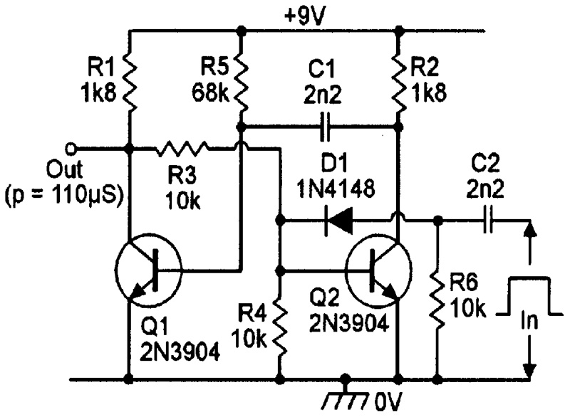
FIGURE 12. Electronically triggered monostable.
The Figure 12 and 13 circuits each give an output pulse period of about 110 mS with the component values shown. The period can be varied from a fraction of a millisecond to many seconds by choice of the C1-R5 values. The circuits can be triggered by sine or other non-rectangular waveforms by feeding them to the monostable input via a Schmitt trigger or similar sine/square converter circuit (see Figure 20).
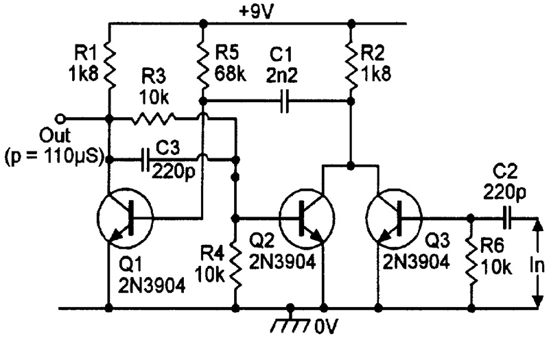
FIGURE 13. Monostable with gate-input triggering.
BISTABLE CIRCUITS
Bistable multivibrators make good stop/go waveform generators, and Figure 14 shows a basic manually-triggered version of such a circuit, which is also known as an R-S (Reset-Set) flip-flop. Its output can be set to the high state by briefly closing S1 (or by applying a negative pulse to Q1 base via a current-limiting resistor), thus turning Q1 off (and simultaneously turning Q2 on via the R3 cross-coupling), and the circuit then latches into this state until it is reset to the low state by briefly closing S2 (or by applying a negative current-limited pulse to Q2 base), thus turning Q2 off and therefore turning Q1 on via the R4 cross coupling. The circuit then latches into this new state until it is set again via S1, and so on.
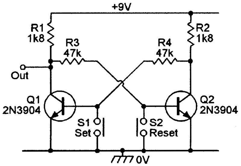
FIGURE 14. Basic manually-triggered R-S bistable multivibrator.
The latching action of the basic Figure 14 circuit relies on the fact that the saturation voltage (typically 200 mV) of the ON transistor is significantly lower than the base-biasing voltage (typically 600 mV) of the opposing device. In practice, these ideal conditions may not be met if the transistor is not a good-quality silicon type, or if it operates at an excessive temperature or with a low-value collector load. In cases of doubt, the circuit’s reliability can be greatly enhanced by using the modifications shown in the improved circuit of Figure 15, in which resistors R5 and R6 act as simple potential dividers with R3 and R4, respectively, thus reducing the undesirable effects of high saturation voltages, etc.
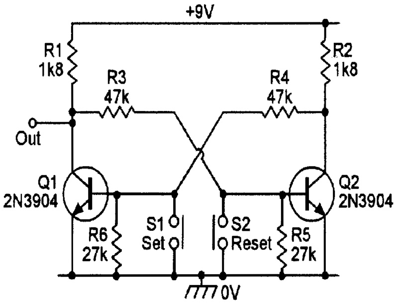
FIGURE 15. Improved manually-triggered R-S bistable multivibrator with switch-low triggering.
The circuits of Figures 14 and 15 both give a switch-low triggering action, in which the circuit changes state when an ON transistor is turned OFF by pulling its base low via a switch or by applying a negative pulse to its base.
Figure 16 shows an alternative version of the basic manually-triggered bistable, in which the circuit gives a switch-high action in which the circuit changes state when an OFF transistor is turned ON by pulling its base high via a switch or by applying a positive current-limited pulse to its base.
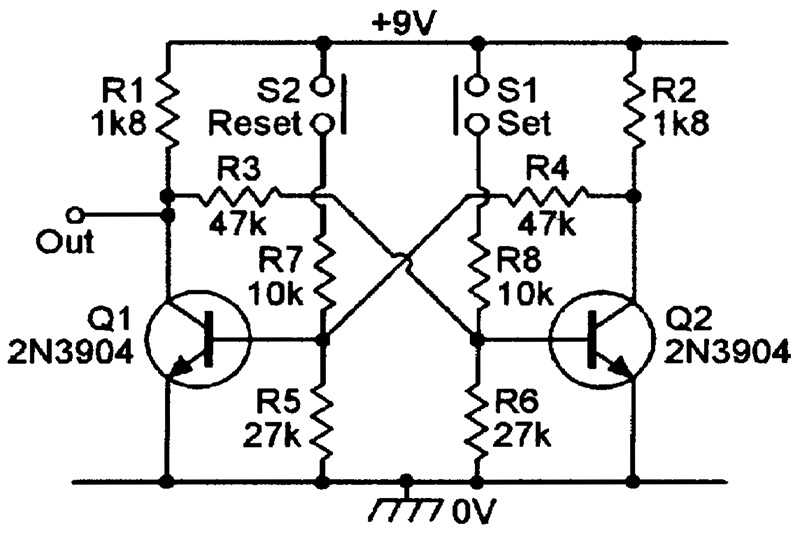
FIGURE 16. Manually-triggered R-S bistable with switch-high triggering.
Note that when power is initially applied to the basic Figure 14 to 16 circuits, the output initially settles into a randomly-determined state that depends on the relative characteristics of the two transistors and their associated passive components.
If desired, the basic circuit can be made to automatically switch into a desired initial power up state by automatically feeding a suitable switch-on trigger pulse to the base of one or the other of the two transistors, as shown in Figure 17, which shows the basic Figure 15 circuit modified (via R7-C1 and current-limiting resistor R8) so that the circuit automatically switches into the set (Q1 output high) state at power-up.
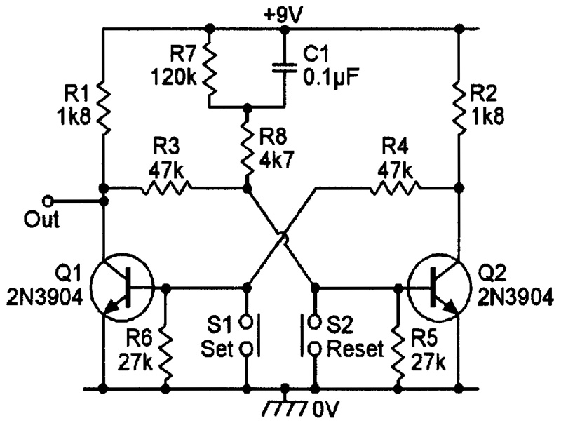
FIGURE 17. Basic Figure 15 circuit modified to give SET action at initial power-up.
One of the most useful applications of the basic bistable multivibrator is as a push-button-controlled timer circuit, in which the output automatically goes high at power-up or on the closure of a push-button start switch, but goes low again automatically after a pre-set delay. Figure 18 shows the basic Figure 17 circuit modified to give such action. Here, the Q1 output automatically goes high (via R7-C1 and R8) at the moment of initial power-up, thereby activating (via emitter follower Q3) an adjustable delayed-pulse generator, which automatically feeds a reset pulse to Q1 base via D1-R9 at the end of the desired delay period, thereby completing the circuit’s operating cycle.
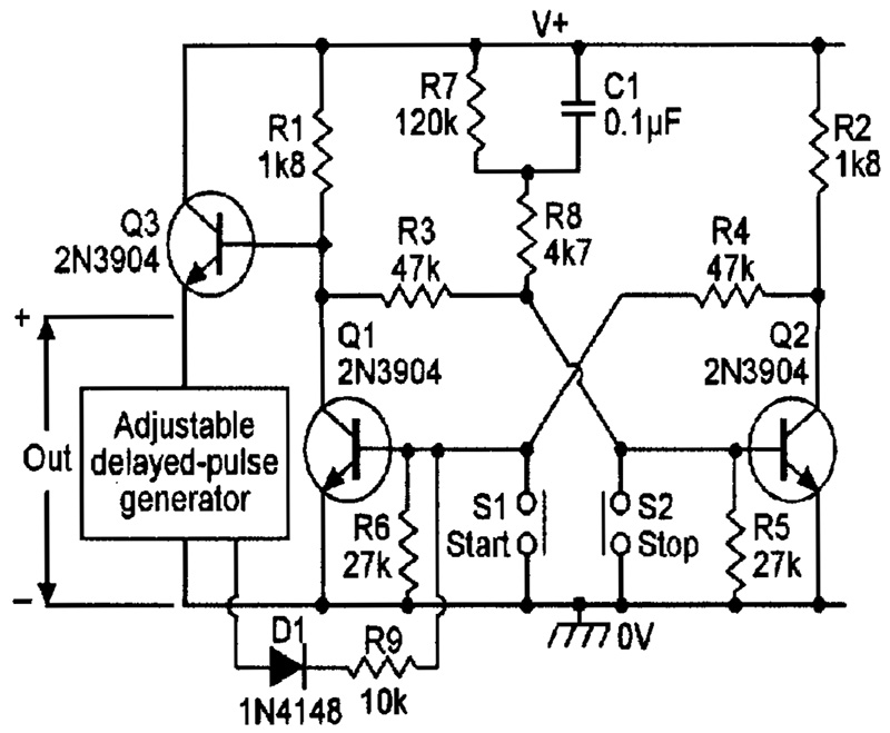
FIGURE 18. Basic circuit of a manually-triggered bistable multivibrator with timed auto-reset action.
Finally, before leaving the basic bistable multivibrator circuit, note that it can, by connecting two steering diodes and associated components as shown in Figure 19, be modified to give a divide-by-two or counting action in which it changes state each time a negative-going trigger pulse is applied. The circuit generates a pair of anti-phase outputs, known as Q and not-Q (denoted by a bar over the Q sign in the diagram). In practice, greatly improved versions of this counting type of circuit are readily available in CMOS or TTL digital IC form.
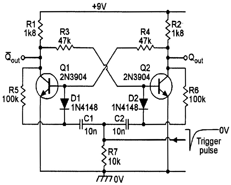
FIGURE 19. Divide-by-two bistable circuit.
THE SCHMITT TRIGGER
The final member of the multivibrator family is the Schmitt trigger. This is a voltage-sensitive bistable switching circuit that changes its output state when the input goes above or below pre-set upper and lower threshold levels; to complete this month’s discussion, Figure 20 shows a simple Schmitt trigger circuit used as a sine-to-square waveform converter that gives a good performance up to a few hundred kHz and needs a sine wave input signal amplitude of at least 0.5V RMS.
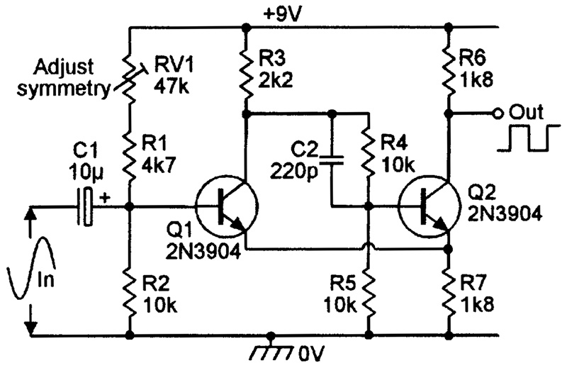
FIGURE 20. Schmitt sine/square converter.
The output signal symmetry varies with input signal amplitude; RV1 should be adjusted to give best results. Next month, we’ll describe a variety of audio power amplifier circuits and associated gadgets. NV