One of the most popular applications of transistors is in audio power amplifiers. This month we describe the operating principles of various circuits of this type and present a selection of practical audio power amplifier circuit designs. The installment concludes by presenting a practical 'scratch and rumble' filter circuit, which can be used to eliminate these unwanted sounds when playing old-fashioned records/discs through any type of audio power amplifier system.
POWER AMPLIFIER BASICS
A transistor power amplifier's job is that of converting a medium-level medium-impedance AC input signal into a high-level low-impedance state suitable for driving a low-impedance external load. This action can be achieved by operating the transistor(s) in either of two basic modes, known as 'class-A' or 'class-B.'
Figure 1(a) shows a basic class-A audio amplifier circuit; Q1 is a common-emitter amplifier with a loudspeaker collector load, and is so biased that its collector current has a quiescent value halfway between the desired maximum and minimum swings of output current, as shown in Figure 1(b), so that maximal low-distortion output signal swings can be obtained. The circuit consumes a high quiescent current, and is relatively inefficient; 'efficiency' is the ratio of AC power feeding into the load, compared with the DC power consumed by the circuit, and at maximum output power is typically about 40%, falling to 4% at one tenth of maximum output, etc.
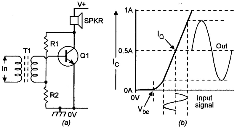
FIGURE 1. Basic circuit (a) and transfer characteristics (b) of a class-A amplifier.
Figure 2 shows an example of a low-power (up to a few dozen milliwatts) high-gain general-purpose class-A amplifier that draws a quiescent current of about 20 mA and is suitable for driving a medium impedance (greater than 65Ω) loudspeaker or headset. Q1 and Q2 are wired as direct-coupled common-emitter amplifiers, and give an overall voltage gain of about 80 dB. Q1's base bias is derived (via R2) from Q2's emitter, which is decoupled via C3 and thus 'follows' the mean collector voltage of Q1. The bias is thus stabilized by DC negative feedback. Input pot RV1 acts as the circuit's volume control.
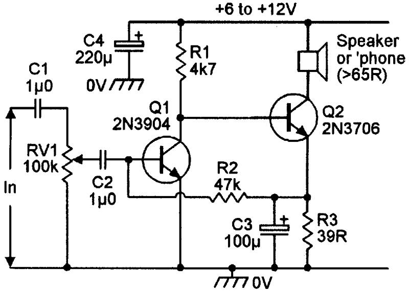
FIGURE 2. General-purpose high-gain low-power audio amplifier.
A basic class-B amplifier consists of a pair of transistors, driven in anti-phase but driving a common output load, as shown in Figure 3(a). In this particular design, Q1 and Q2 are wired in the common-emitter mode and drive the loudspeaker via push-pull transformer T2, and the anti-phase input drive is obtained via phase-splitting transformer T1. The essential features of this type of amplifier are that both transistors are cut off under quiescent conditions, that neither transistor conducts until its input drive signal exceeds its base-emitter 'knee' voltage, and that one transistor is driven on when the other is driven off, and vice versa. The circuit consumes near-zero quiescent current, and has high efficiency (up to 78.5%) under all operating conditions, but it generates severe cross-over distortion in the amplifier's output signal, as shown in Figure 3(b). The basic class-B circuit must thus be modified if it is to be used as a practical audio power amplifier; the modified circuit is known as a 'class-AB' amplifier.
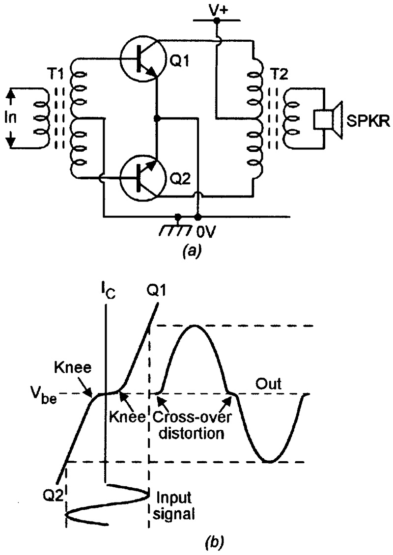
FIGURE 3. Basic circuit (a) and transfer characteristics (b) of a class-B amplifier.
CLASS-AB BASICS
The cross-over distortion of the class-B amplifier can be eliminated by applying slight forward bias to the base of each transistor, as shown in Figure 4, so that each transistor passes a modest quiescent current. Such a circuit is known as a class-AB amplifier. Circuits of this type were widely used in early transistor power amplifier systems but are now virtually obsolete, since they require the use of transformers for input phase-splitting and output loudspeaker driving, and must have closely matched transistor characteristics if a good low-distortion performance is to be obtained.
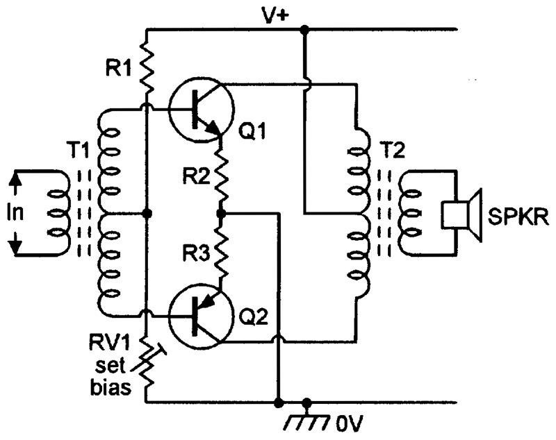
FIGURE 4. Basic circuit of a class-AB amplifier.
Figure 5 shows the basic circuit of a class-AB amplifier that suffers from none of the snags mentioned above. It is a complementary emitter follower, and is shown using a split (dual) power supply. Q1 and Q2 are biased (via R1-RV1-R2) so that their outputs are at zero volts and zero current flows in the loudspeaker load under quiescent conditions, but have slight forward bias applied (via RV1), so that they pass modest quiescent currents and thus do not suffer from cross-over distortion problems. Identical input signals are applied (via C1 and C2) to the bases of both emitter followers. This circuit's operation was described in Part 2 of this 'Cookbook' series.
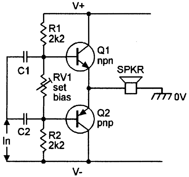
FIGURE 5. Basic class-AB amplifier with complementary emitter follower output and dual power supply.
The basic Figure 5 circuit does not require the use of transistors with closely matched electrical characteristics, and gives direct drive to the speaker. It can be modified for use with a single-ended power supply by simply connecting one end of the speaker to either the zero or the positive supply rail, and connecting the other end to the amplifier output via a high-value blocking capacitor, as shown in Figure 6.
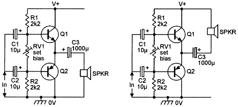
FIGURE 6. Alternative versions of the class-AB amplifier with a single-ended power supply.
The basic Figure 5 and 6 circuits form the basis of virtually all modern audio power amplifier designs, including those in IC form. Many modifications and variations can be made to the basic circuit.
CIRCUIT VARIATIONS
The Figure 5 circuit gives unity overall voltage gain, so an obvious circuit modification is to provide it with a voltage-amplifying driver stage, as in Figure 7. Here, common emitter amplifier Q1 drives the Q2-Q3 complementary emitter followers via collector load resistor R1 and auto-biasing silicon diodes D1 and D2 (the function of these diodes was explained in Part 2 of this series). Q1's base bias is derived from the circuit's output via R2-R3, thus providing DC feedback to stabilize the circuit's operating points, and AC feedback to minimize signal distortion. In practice, a pre-set pot is usually wired in series with D1-D2, to enable the Q2-Q3 bias to be trimmed; low-value resistors R4 and R5 are wired in series with Q2 and Q3 emitters to prevent thermal runaway, etc.
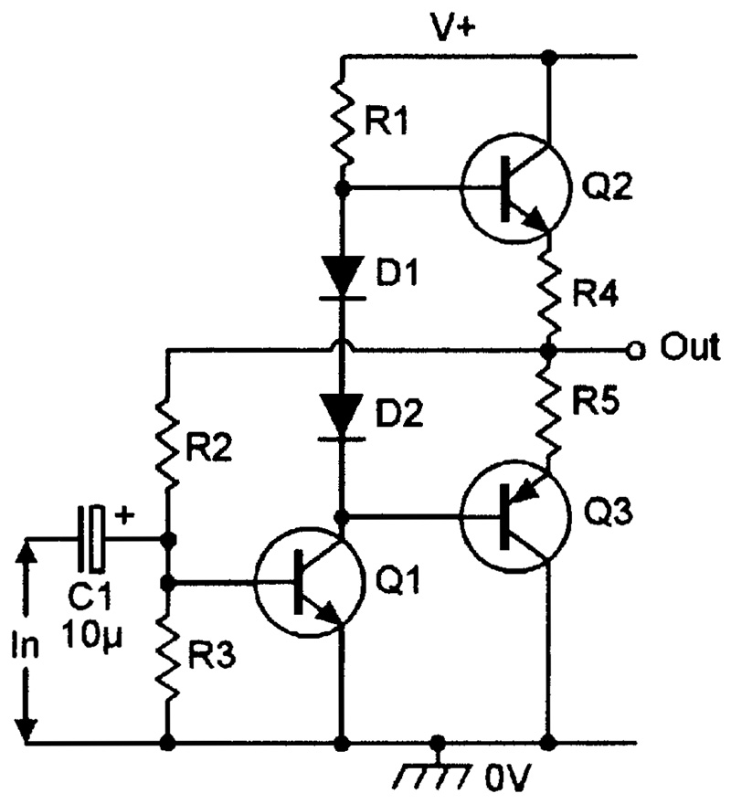
FIGURE 7. Complementary amplifier with driver and auto-bias.
The input impedance of the basic Figure 5 circuit equals the product of the loudspeaker load impedance and the hfe of Q1 or Q2. An obvious circuit improvement is to replace the individual Q1 and Q2 transistors with high-gain pairs of transistors, to increase the circuit's input impedance, and enable it to be used with a driver with a high-value collector load. Figures 8 to 10 show three alternative ways of modifying the Figure 7 circuit in this way.
In Figure 8, Q2-Q3 are wired as a Darlington NPN pair, and Q3-Q4 as a Darlington PNP pair; note that four base-emitter junctions exist between Q2 base and Q4 base, so this output circuit must be biased via a chain of four silicon diodes.
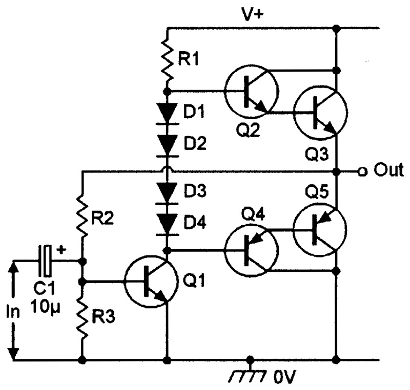
FIGURE 8. Amplifier with Darlington output stages.
In Figure 9, Q2-Q3 are wired as a Darlington NPN pair, but Q3-Q4 are wired as a complementary pair of common-emitter amplifiers that operate with 100% negative feedback and provide unity voltage gain and a very high input impedance. This design is known as a 'quasi-complementary' output stage, and is probably the most popular of all class-AB amplifier configurations; it calls for the use of three biasing diodes.
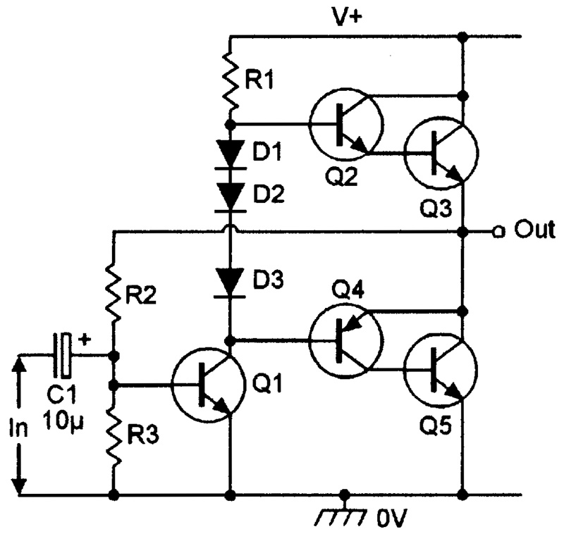
FIGURE 9. Amplifier with quasi-complementary output stages.
In Figure 10, both Q2-Q3 and Q4-Q5 are wired as complementary pairs of unity-gain common-emitter amplifiers with 100% negative feedback; they are mirror images of each other, and form a complementary output stage that needs only two biasing diodes.
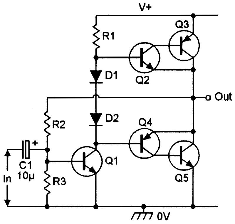
FIGURE 10. Amplifier with complementary output stages.
The circuits of Figures 7 to 10 all call for the use of a chain of silicon biasing diodes. If desired, each of these chains can be replaced by a single transistor and two resistors, wired in the 'amplified diode' configuration described in Part 2 of this series and repeated here, in very basic form, in Figure 11.
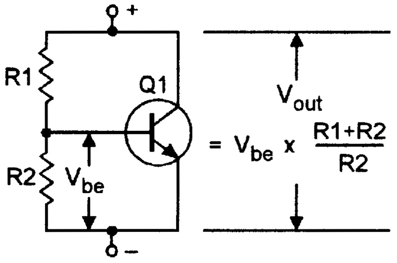
FIGURE 11. Fixed-gain amplified diode circuit.
Thus, if R1 is shorted out, the circuit acts like a single base-emitter junction diode, and if R1 is not shorted out, it acts like (R1+R2)/R2 series-wired diodes. Figure 12 shows the circuit modified so that it acts as a fully adjustable amplified silicon diode, with an output variable from 1 to 5.7 base-emitter junction voltages.
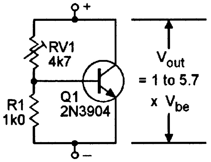
FIGURE 12. Adjustable amplified diode circuit.
In Figure 13, the Q1 collector load comprises R1 and R2 in series, and the circuit's output signal (which also appears across SPKR), is fed back to the R1-R2 junction via C2, thus bootstrapping R2's value so that its AC impedance is boosted by (typically) a factor of about 20, and the circuit's voltage gain is boosted by a similar amount.
FIGURE 13. Amplifier with bootstrapped driver stage.
Another useful modification that can be made to the basic Figure 7 circuit is to add bootstrapping to its R1 collector load, to boost its effective impedance and thus raise the circuit's overall voltage gain (the 'bootstrapping' technique was also described in Part 2 of this series). Figures 13 and 14 show examples of bootstrapped class-AB power amplifier circuits.
Figure 14 shows a version of the circuit that saves two components; in this case, the SPKR forms part of Q1's collector load, and directly bootstraps R1.
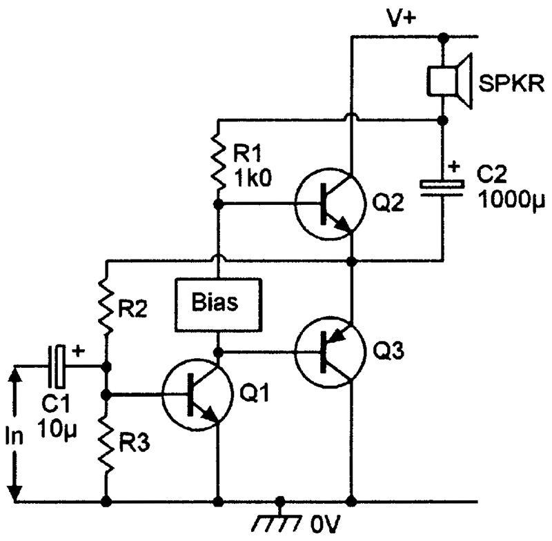
FIGURE 14. Alternative amplifier with bootstrapped driver stage.
PRACTICAL CLASS AB AMPLIFIERS
The easiest way to build a class-AB audio amplifier is to do so using one of the many readily-available audio ICs of this type. In some cases, however, particularly when making 'one off' projects, it may be cheaper or more convenient to use a discrete transistor design, such as one of those shown in Figures 15 or 16.
Figure 15 shows a simple class-AB amplifier that can typically drive 1W into a 3Ω speaker. Here, common-emitter amplifier Q1 uses collector load LS1-R1-D1-RV2, and drives the Q2-Q3 complementary emitter follower stage. The amplifier's output is fed (via C2) to the LS1-R1 junction, thus providing a low impedance drive to the loudspeaker and simultaneously bootstrapping the R1 value so that the circuit gives high voltage gain. The output is also fed back to Q1 base via R4, thus providing base bias via a negative feedback loop. In use, RV1 should be trimmed to give minimal audible cross-over distortion consistent with low quiescent current consumption (typically in the range 10 mA to 15 mA).
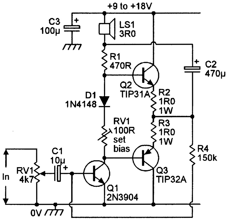
FIGURE 15. Simple 1 watt amplifier.
Figure 16 shows a rather more complex audio power amplifier that can deliver about 10W into an 8Ω load when powered from a 30 V supply.
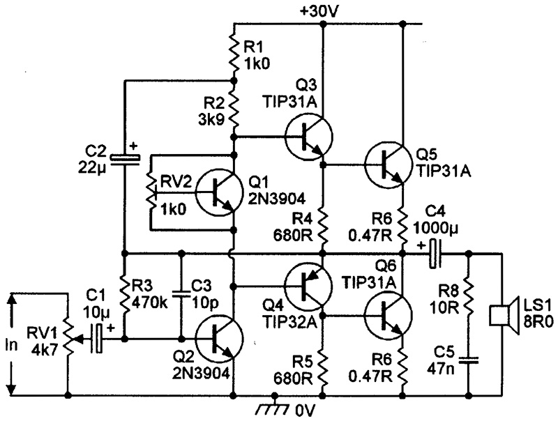
FIGURE 16. 10 watt audio amplifier.
This circuit uses high-gain quasi-complementary output stages (Q3 to Q6) and uses an adjustable amplifier diode (Q1) as an output biasing device. The Q2 common emitter amplifier stage has its main load resistor (R2) bootstrapped via C2, and is DC biased via R3, which should set the quiescent output voltage at about half-supply value (if not, alter the R3 value). The upper frequency response of the amplifier is restricted via C3, to enhance circuit stability, and C5-R8 are wired as a Zobel network across the output of the amplifier to further enhance the stability. In use, the amplifier should be initially set up in the way already described for the Figure 15 circuit.
ALTERNATIVE DRIVERS
In the basic Figure 7 circuit, the Q1 driver stage uses parallel DC and AC voltage feedback via potential divider network R2-R3. This circuit is simple and stable, but suffers from fairly low gain and very low input resistance, and can be used over only a very limited range of power supply voltages. A simple variation of this circuit is shown in Figure 17. It uses current feedback via R1-R2, thus enabling the circuit to be used over a wide range of supply voltages.
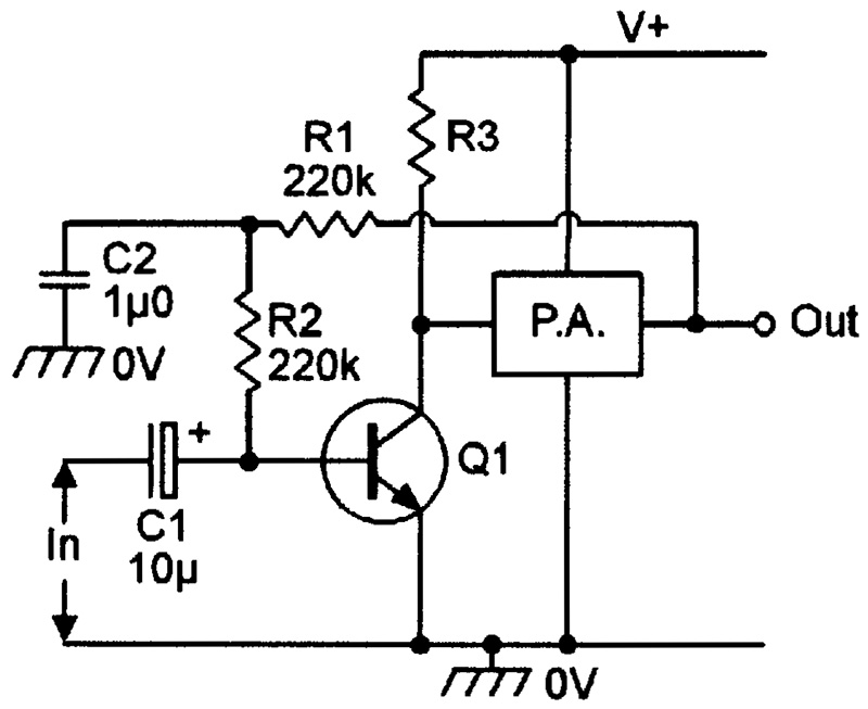
FIGURE 17. Driver stage with decoupled parallel DC feedback.
The feedback resistors can be AC-decoupled (as shown) via C2 to give increased gain and input impedance, at the expense of increased distortion. Q1 can be a Darlington type, if a very high input impedance is required.
Figure 18 shows an alternative configuration of driver stage. This design uses series DC and AC feedback, and gives greater gain and input impedance than the basic Figure 7 circuit, but uses two transistors of opposite polarities.
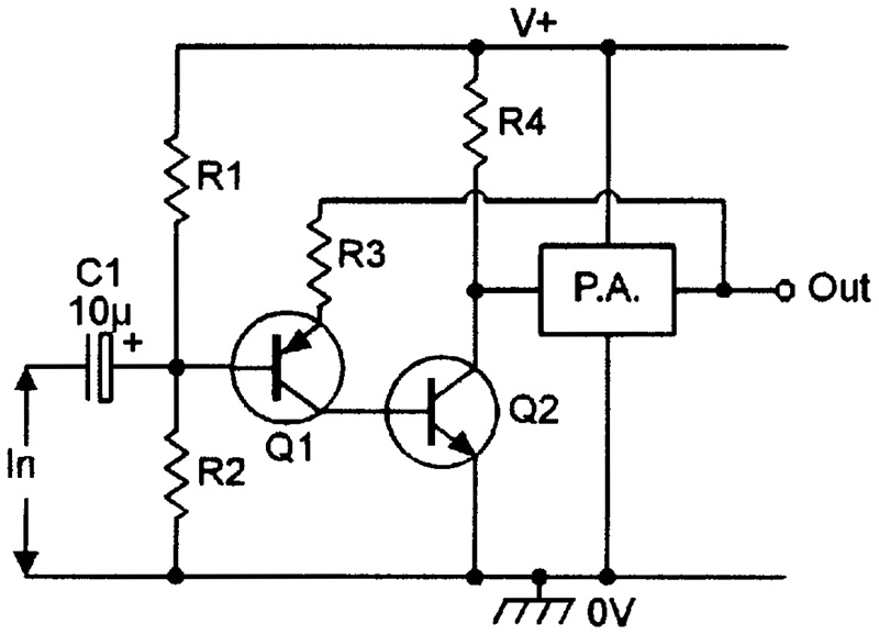
FIGURE 18. Driver stage with series DC feedback.
Finally, to complete this look at audio power amplifiers, Figure 19 shows a circuit that has direct-coupled ground-referenced inputs and outputs, and uses split power supplies. It has a long-tailed pair input stage, and the input and output both center on zero volts if R1 and R4 have equal values. The circuit can be used with a single ended power supply by grounding one supply line and using AC coupling of the input and output signals. This basic circuit forms the basis of many IC power amplifier designs.
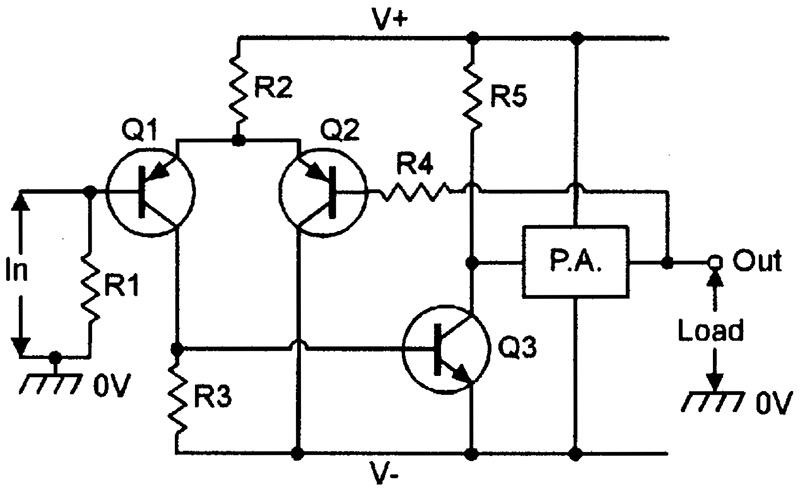
FIGURE 19. Driver stage with long-tailed pair input.
SCRATCH/RUMBLE FILTERS
A common annoyance when playing old records (discs) through audio power amplifiers is that of scratch and/or rumble sounds. The scratch noises are mainly high-frequency (greater than 10 kHz) sounds picked up from the disc surface, and the rumbles are low-frequency (less than 50 Hz) sounds that are mostly caused by slow variations in motor-drive speed.
Each of these noises can be greatly reduced or eliminated by coupling the player's audio signals into the audio power amplifier input via a filter that rejects the troublesome parts of the audio spectrum. Figures 20 and 21 show suitable circuits.
The high-pass rumble filter of Figure 20 gives unity voltage gain to signals above 50 Hz, but gives 12dB per octave rejection to those below this value, i.e., it gives 40dB of attenuation at 5 Hz, etc. Emitter-follower Q1 is biased at half-supply volts from the R1-R2-C3 low-impedance point, but has negative feedback applied via the R3-C2-C1-R4 filter network. The circuit's frequency turn-over point can be altered by changing the C1-C2 values (which must be equal); thus, if the C1-C2 values are halved (to 110nF), the turn-over frequency doubles (to 100 Hz), etc.
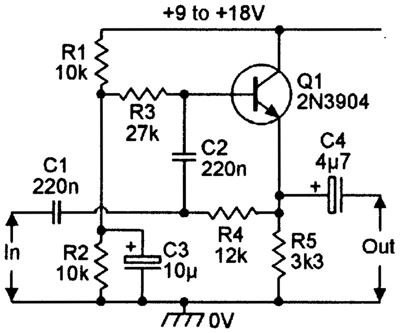
FIGURE 20. 50 Hz rumble or high-pass filter.
The low-pass scratch filter of Figure 21 gives unity voltage gain to signals below 10 kHz, but gives 12dB per octave rejection to those above this value.
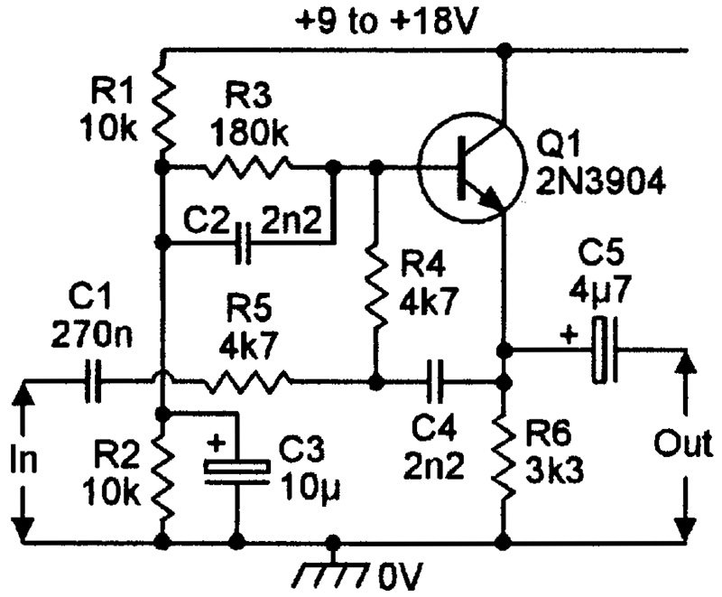
FIGURE 21. 10 kHz scratch or low-pass filter.
This circuit is similar to that of Figure 20, except that the positions of the resistors and capacitors are transposed in the C2-R4-C4-R5 filter network. The circuit's turn-over frequency can be altered by changing the C2-C4 values, e.g., values of 3.3nF give a frequency of 7.5 kHz.
The Figure 20 and 21 circuits can be combined to make a composite scratch and rumble filter, by connecting the output of the high-pass filter to the input of the low-pass filter; if desired, the filters can be provided with bypass switches, enabling them to be easily switched in and out of circuit, by using the connections of Figure 22.
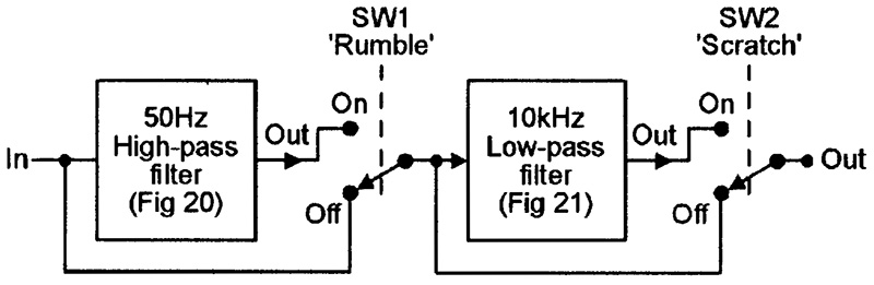
FIGURE 22. Complete scratch/rumble filter, with switching.
Note that if the Figure 20 and 21 designs are to be built as a single unit, a few components can be saved by making the R1-R2-C3 biasing network common to both circuits.
The next, (and final) installment will describe a miscellaneous collection of useful transistor circuits and gadgets. NV