INTRODUCTION
In many modern battery-powered electronic circuits, a DC supply is needed that is of either a larger voltage value than that of the main battery, or is of reverse polarity; a circuit that is powered from a six-volt battery may, for example, incorporate a single op-amp stage that needs +12V and -6V supply lines. In such cases, the required voltages may be generated via one or more special DC voltage converter circuits.
Most electronic DC voltage converters operate in one or another of four basic ways and use a DC-powered oscillator to drive either a simple diode-capacitor ‘voltage multiplier’ network, or a step-up transformer and rectifier network, or a ‘flying capacitor’ voltage converter, or a ‘diode-steered charge pump,’ which produces the desired final DC output voltage or voltages.
This article explains the operating principles of — and shows practical examples of — each of these four basic types of circuits.
DC ‘VOLTAGE MULTIPLIER’ CIRCUITS
BASIC PRINCIPLES
Conventional DC ‘voltage multiplier’ types of voltage converter circuits are based on a simple two-section diode-capacitor type of rectifier network that was originally designed way back in the 1930s for use in high-value AC-to-DC voltage conversion applications, and is still widely used today.
To understand this circuit’s basic operation and terminology (which can sometimes be rather confusing), it is necessary to start off by looking at a simple AC-to-DC power conversion circuit, as follows:
The simplest AC-to-DC power conversion circuit is the basic half-wave rectifying type shown in Figure 1, which depicts a circuit that uses a transformer with a secondary voltage value of 250V rms.
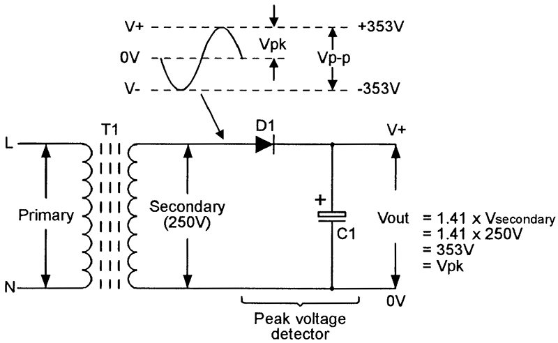
FIGURE 1. Basic details of a simple 250V half-wave rectified DC power supply.
Here, the AC voltage applied to the input of rectifier D1 swings alternately above and below the 0V value, rising to a positive Vpeak (Vpk) value +353V in the positive half-cycle, and falling to a negative Vpeak value of -353V in the negative half-cycle.
D1 is forward-biased during each positive half-cycle and thus charges capacitor C1 to a peak value of (ignoring D1’s forward volt drop) +353V, but is reverse-biased during each negative half-cycle, which thus has no practical effect on the circuit.
This circuit produces a positive output voltage, but can be made to generate a negative output voltage by simply reversing the polarities of D1 and C1.
The really important thing to note about the Figure 1 half-wave rectifier circuit is that D1 and C1 act together as a peak-voltage detector that makes the circuit give an output equal to the positive peak value of T1’s secondary voltage.
The same basic action occurs in all conventional full-wave rectifier circuits, which also give an output equal to the peak value of the transformer’s secondary voltage.
During the early 1930s, engineers needed a cheap, reliable, and safe way of generating high-value low-power DC voltages from low-cost non-lethal transformers, and devised a simple two-section ‘voltage multiplier’ circuit to do this job. Figure 2 shows such a circuit, driven from the secondary winding of a 250V transformer.
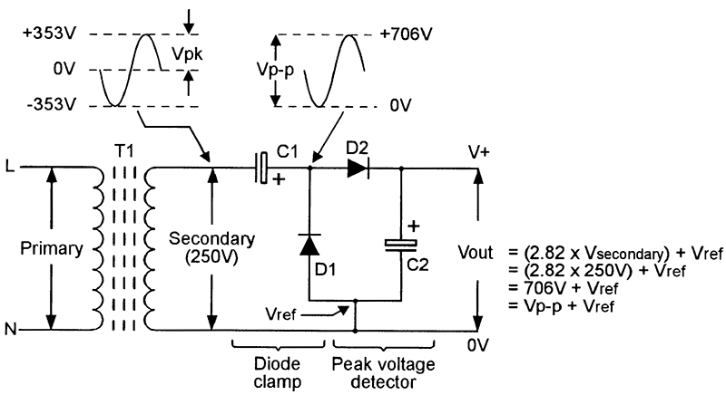
FIGURE 2. Basic details of a transformer-driven ‘voltage-doubling’ voltage multiplier circuit.
Here, the C1-D1 section acts as a diode clamp that, when fed with a normal AC input that swings symmetrically about the 0V value, produces an output waveform that is of identical shape, but has its peak negative point clamped to the 0V ‘reference’ value, as shown in the diagram.
This waveform’s peak output value equals the peak-to-peak (Vp-p) value of the AC input voltage, and is fed directly into the input of the simple D2-C2 peak voltage detector section, which thus produces a DC output voltage equal to the Vp-p value (rather than the peak value) of the AC input voltage.
This circuit thus gives twice as much output voltage as a conventional half-wave or full-wave rectifier circuit, and is thus known as a ‘voltage-doubling’ voltage multiplier.
The circuit can be made to generate a negative (rather than positive) output voltage by simply reversing the polarities of C1-D1 and D2-C2.
One very important point to note about the basic Figure 2 circuit is that its output voltage actually equals Vp-p plus the common ‘reference’ voltage (Vref) of D1-C2, which in this particular example is 0V. Thus, if this circuit is modified so that Vref is somehow raised to (say) +1000V, the 706V output of C2 will be added to that of Vref to give a final output voltage of 1,706V, and so on.
The heart of the Figure 2 circuit is the actual C1-D1-D2-C2 voltage doubler network. Figure 3(a) shows the conventional diagram of this network and Figure 3(b) shows it redrawn as a ‘standard’ voltage-doubling voltage multiplier section.
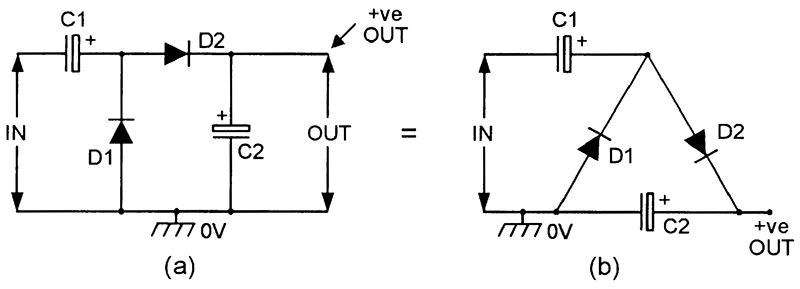
FIGURE 3. (a) Conventional voltage-doubler diagram, and (b) the circuit redrawn in ‘standard’ form.
A major feature of the voltage-doubler is that numbers of ‘doublers’ can easily be interconnected to give various values of voltage multiplication, and such circuits are best drawn by using the standard Figure 3(b) representation.
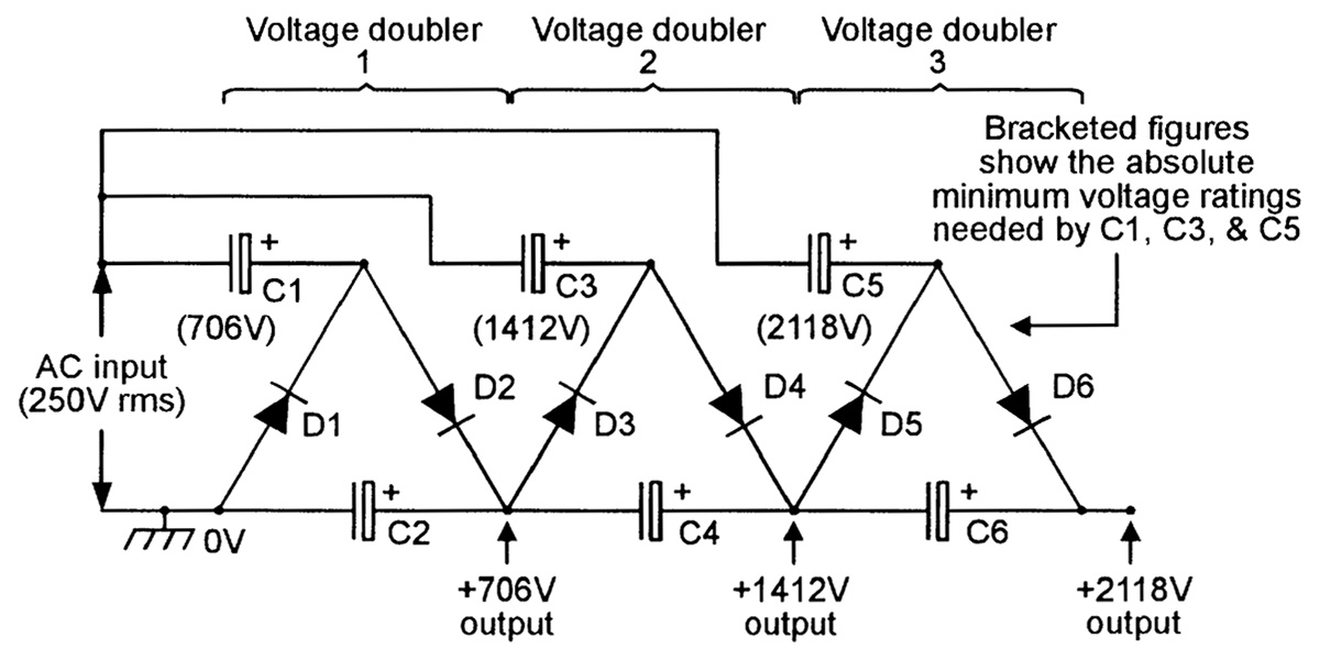
Figure 4, for example, shows three of these ‘doubler’ stages interconnected to give a voltage sextupler action in which the final output voltage is six times greater than the peak value of the original 250V rms input voltage.
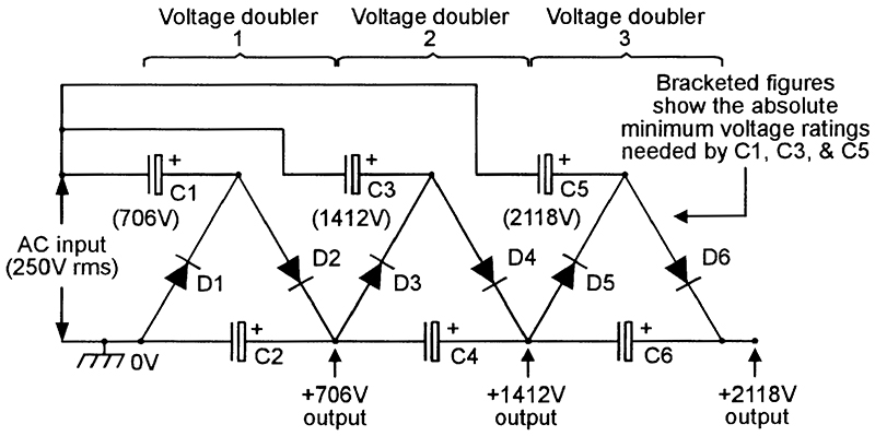
FIGURE 4. Three ‘doublers’ interconnected to give x6 voltage multiplication.
Here, each ‘doubler’ section generates an individual output (across its C2, C4, or C6 capacitor) of 706V, but the output of the first doubler acts as the Vref point of the second doubler, and the output of the second doubler acts as the Vref point of the third doubler, the net effect being that the three individual output voltages add together to give a final DC output of +2118V from the 250V AC input.
Note in the Figure 4 circuit that the input capacitor of each section is fed directly from the AC input voltage, and needs an absolute minimum voltage rating equal to that section’s output-to-ground voltage, e.g., C5 needs a minimum rating of 2118V.
In the mid 1930s a modified version of the voltage multiplier was designed to overcome this snag. Known as the Cockcroft-Walton voltage multiplier, it uses standard voltage-doubler stages interconnected in the manner shown in Figure 5.

FIGURE 5. This three-stage Cockcroft-Walton circuit gives x6 voltage multiplication.
This circuit is similar to that of Figure 4, except that the input of each doubler (except the first) is fed from the ‘clamped’ AC voltage point of the preceeding doubler.
Consequently, the ‘minimum voltage rating’ requirement of each component used in each doubler stage equals the peak-to-peak value of the original AC input voltage.
A weakness of the Cockcroft-Walton voltage multiplier is that its output impedance is rather high (it is proportional to the sum of the impedances of the various input capacitors), and it can thus supply only small output currents.
In practice, this type of voltage multiplier was originally designed simply to generate a very high (up to about 30KV) accelerator voltage on the final anode of cathode-ray tubes, an application which requires very little energizing current.
Note that a 10-stage circuit of this type — when driven by a 500V AC input — generates a DC output of over 14KV, but the components used in each stage have minimum voltage rating requirements of less than 1.5KV.
PRACTICAL CIRCUITS
A DC voltage can easily be converted into one of greater value or of reversed polarity by using the DC supply to power a free-running 1KHz to 30KHz squarewave generator that has its output fed to a voltage multiplier of one of the basic types already described, which thus provides the desired ‘converted’ DC output voltage. Figure 6 shows a practical demonstration circuit of this type.
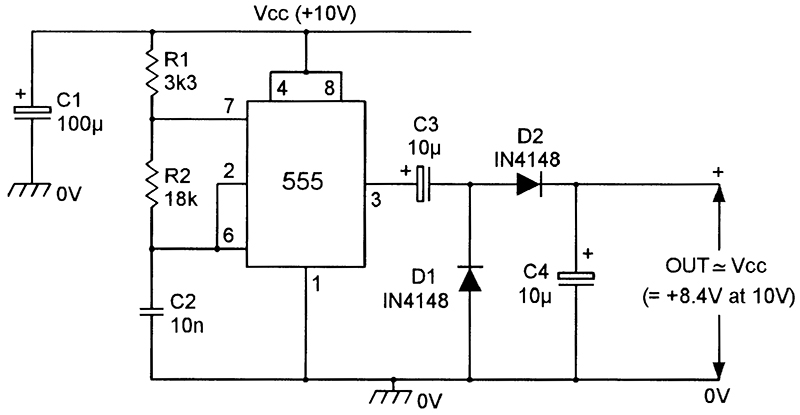
FIGURE 6. Basic ‘voltage doubler’ demonstration circuit.
The Figure 6 circuit uses a type-555 ‘timer’ IC (which can supply fairly high output currents) as a free-running squarewave generator that operates at about 3KHz (determined by the R1-R2-C2 values), and directly drives the C3-D1-D2-C4 ‘doubler’ stage, which (ideally) produces a DC output equal to the peak-to-peak output of the squarewave, which (ideally) equals the Vcc value.
In practice, the squarewave’s peak-to-peak value is slightly less than Vcc, and the ‘doubler’ loses another 1.2V in volt-drops in D1 and D2, the net result being that the actual output (when very lightly loaded) is about 1.6V less than Vcc, e.g., 8.4V with a 10V supply. The circuit can use any supply in the range 5V to 15V.
Figure 7 shows a far more useful version of the basic Figure 6 ‘voltage-doubler’ circuit.

FIGURE 7. DC voltage-doubling circuit.
In this version, the C3-D1-D2-C4 ‘doubler’ is tied to the positive (rather than 0V) supply line, and its output voltage is thus added to that of the supply line, thus giving a DC output voltage (when lightly loaded) of almost two times Vcc.
In practice, the prototype circuit gives an output of almost 19V when using a 10V supply.
Figure 8 shows the Figure 7 circuit modified for use with a cascaded pair of ‘doubler’ stages, in a configuration that is known (because it generates a DC output four times greater than a basic peak AC input voltage) as a ‘voltage quadrupler.’
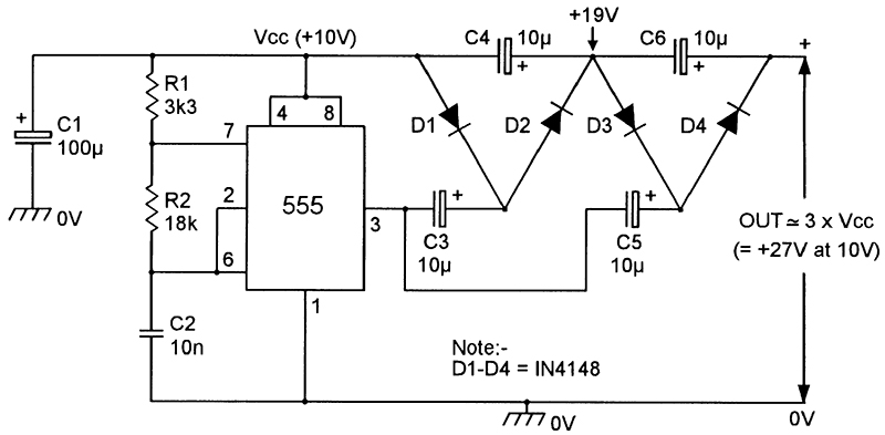
FIGURE 8. Cascaded ‘voltage doubler’ circuit.
Here, the output of the new C5- D3-D4-C6 ‘doubler’ stage (which is a couple of volts less than Vcc) is added to that of the basic Figure 7 circuit, thus giving a DC output voltage (when lightly loaded) of almost three times Vcc.
In practice, the prototype circuit gives an output of 27V when using a 10V supply.
Figure 9 shows a particularly useful type of voltage multiplier circuit that generates a negative output voltage that (ideally) is almost equal in amplitude, but opposite in polarity to that of the IC’s supply line, thus providing a split-supply output from a single-ended input.
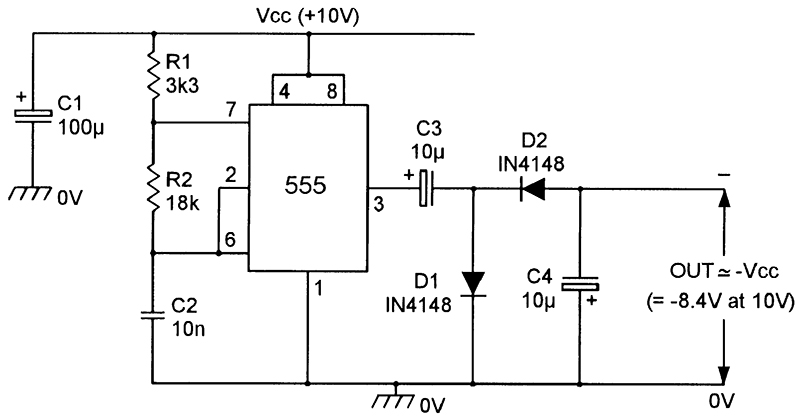
FIGURE 9. DC negative voltage generator.
The circuit is similar to that of Figure 6, but has its D1-D2-C4 ‘doubler’ polarities reversed, so that its output voltage is negative to the 0V line.
In practice, the prototype circuit gives an output of -8.4V when using a 10V supply. (Note: two of these ‘doubler’ stages, when cascaded, give an output of -17.5V when using a 10V supply.)
A HIGH-VOLTAGE GENERATOR CIRCUIT
The ‘voltage multiplier’ method of generating increased values of DC output voltage is usually cost-effective only when multiplier ratios of less than six are needed.
In cases where very large step-up ratios are required (as, for example, when hundreds of volts must be generated via a 6V to 12V supply), it is often better to use the output of a low-voltage oscillator or squarewave generator to drive a step-up voltage transformer, which then provides the required high-value voltage (in AC form) on its secondary (output) winding; this AC voltage can easily be converted back to DC via a simple rectifier-filter network. Figure 10 shows a practical low-power high-voltage generator circuit of this type.

FIGURE 10. 9V to 300V DC-to-DC converter.
The Figure 10 circuit acts as a DC-to-DC converter that generates a 300V DC output from a 9V DC power supply.
Here Q1, and its associated circuitry, act as a Hartley L-C oscillator, with the low-voltage primary winding of 9V-0-9V to 250V mains transformer T1 (or a transformer with a similar turns ratio) forming the ‘L’ part of the oscillator, which is tuned via C2.
The supply voltage is stepped up to about 350V peak at T1 secondary, and is half-wave rectified and smoothed via D1-C3. With no permanent load on C3, the capacitor can deliver a powerful, but non-lethal ‘belt.’
With a permanent load on the output, the output falls to about 300V at a load current of a few milliamps.
‘FLYING CAPACITOR’ DC VOLTAGE CONVERTERS
One very efficient way of obtaining good +ve to -ve low-voltage conversion is to use the so-called ‘flying capacitor’ technique, which is used by the popular ICL7660 dedicated voltage converter IC (and its SI7660, LMC7660, etc., equivalents) and by several similar devices.
The ICL7660 is housed in an eight-pin DIL package as shown in Figure 11(a), and is designed to be powered from a single-ended DC supply that is connected between pins 8 (V+) and 3 (GND or 0V), and to generate an equal-value negative output on pin 5 (-Vout), i.e., if powered from a +5V supply, it generates a -5V output on pin 5, thus making double the supply voltage (i.e., 10V) available between pins 8 and 5.
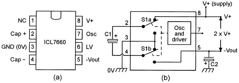
FIGURE 11. (a) Outline and pin notations and (b) simplified basic usage circuit of the ICL7660 voltage converter IC.
The IC can thus be used as either a negative-voltage generator or as a voltage doubler.
The ICL7660 can be used with any +1.5V to 10V DC supply, consumes a typical quiescent current of 170µA at 10V, and has a typical +ve to -ve voltage conversion efficiency of 99.9 percent when its pin 5 output is not loaded.
When the IC’s output is loaded, it acts (at 10V) like a voltage source with an output impedance of about 70R, and can supply maximum output currents of about 40mA; the output impedance is inversely proportional to the supply voltage, and is typically about 330R at 2.5V.
The ICL7660 uses the ‘flying capacitor’ method of voltage conversion that is illustrated in Figure 11(b). The IC houses a CMOS squarewave generator that operates at a basic frequency of about 10KHz and has a symmetrical half-frequency output (available on pin 2) that repeatedly toggles built-in CMOS two-pole change-over switch S1, which is connected to ‘flying’ external capacitor C1.
The circuit action is such that, when S1 is toggled high, C1 is connected directly between the ground and V+ lines (as shown in the diagram) and thus charges up to the full positive supply voltage value.
On the next clock cycle, however, S1 toggles low and, under this condition, C1 is connected — in reverse polarity — directly across external output capacitor C2, thus generating an output voltage of V- across C2. This toggling sequence repeats continuously, at half of the clock-generator frequency.
Note that, since the ICL7660 uses CMOS rather than bipolar semiconductor switches in its ‘conversion’ circuitry, the IC operates with very high-voltage conversion efficiency.
The ICL7660 is an easy device to use, but none of its terminals must ever be connected to a voltage greater than V+ or less than GND (0V).
If the IC is to be used with supplies in the range 1.5V to 3.5V, the pin 6 ‘LV’ terminal (which controls an internal voltage regulator) should be grounded; at supply values greater than 3.5V, pin 6 must be left open circuit. At supply values greater than 6.5V, a protection diode must be wired in series with OUTPUT pin 5.
The circuits of Figures 12 to 20 show a selection of practical designs in which these rules are applied.
ICL7660 CIRCUITS
The most basic applications of the ICL7660 are as a simple negative-voltage generator or as a voltage doubler, and Figures 12 to 14 show three simple circuits of this type; in each case, C1 is a ‘flying’ capacitor and C2 is a smoothing/storage capacitor and each have a value of 10µF.
The Figure 12 voltage converter is intended for use with 1.5V to 3.5V supplies, and requires the use of only two external components.
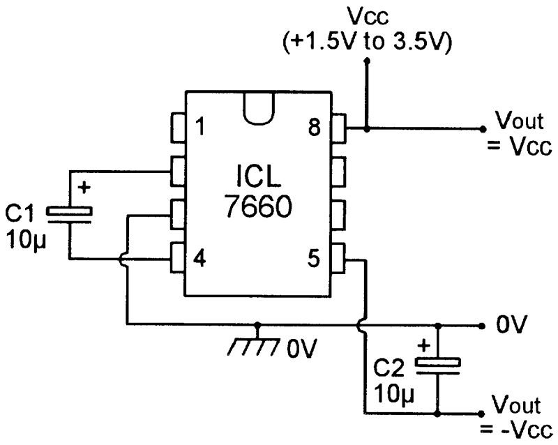
FIGURE 12. DC negative-voltage generator or voltage doubler using 1.5 to 3.5V supply.
The Figure 13 circuit is similar, but is meant for use with supplies in the 3.5V to 6.5V range and thus has pin 6 grounded.
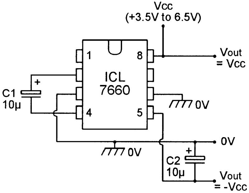
FIGURE 13. DC negative-voltage generator or voltage doubler using 3.5V to 6.5V supply.
Finally, the Figure 14 circuit is meant for use with supplies in the range 6.5V to 10V, and thus has diode D1 wired in series with output pin 5, to protect it against excessive reverse-biasing from C2 when the power supplies are removed.
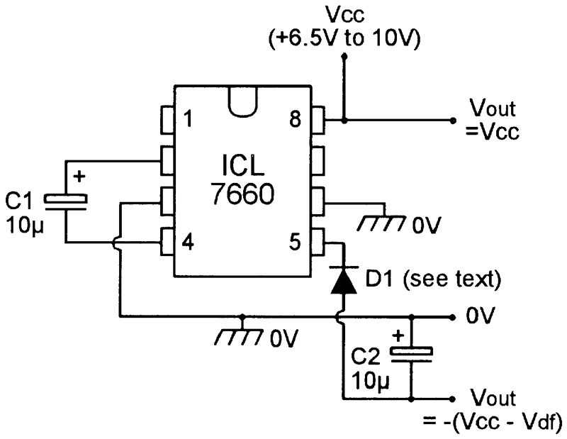
FIGURE 14. DC negative-voltage generator or voltage doubler using 6.5 to 10V supply.
The presence of this diode reduces the available output voltage by Vdf, the forward volt drop of the diode; to keep this volt drop to minimum values, D1 should be a germanium or Schottky type.
A useful feature of the ICL7660 is that numbers of these ICs (up to a maximum of 10) can be cascaded to give voltage conversion factors greater than unity. Thus, if three stages are cascaded, they give a final negative output voltage of -3Vcc, etc. Figure 15 shows the connections for cascading two of these stages; any additional stages should be connected in the same way as the right-hand IC of this diagram.
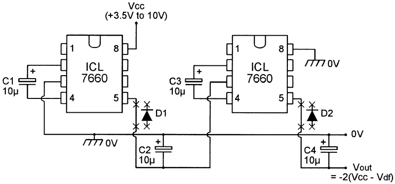
FIGURE 15. Cascading ICs for increased negative output voltage.
It has already been pointed out that a single ICL7660 IC can be used as a highly efficient voltage doubler that can, for example, generate a centre-tapped 10V output when powered from a single-ended 5V input.
Figure 16 shows how two of these ICs can be cascaded to generate a centre-tapped 12V output when the circuit is powered from a single-ended 3V source (e.g., from two series-connected 1.5V cells).
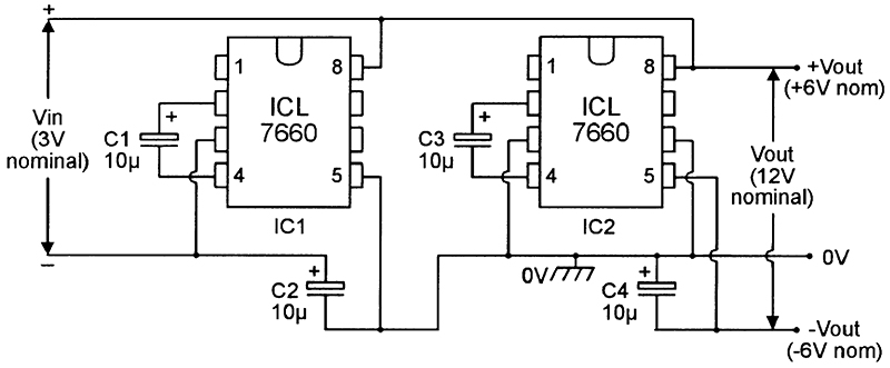
FIGURE 16. Cascaded ICs giving a centre-tapped 12V output from a 3V supply.
Here, IC1 is used as a basic voltage doubler, powered from a 3V source connected between pins 3 and 8, and its 6V output (from between pins 5 and 8) is used to power IC2 via pins 3 and 8, and IC2 thus generates an output (between pins 5 and 8) of 12V when very lightly loaded. This 12V output has a source impedance of about 500R, and falls by about 0.5V per mA increase in load current (most of this volt drop is reflected from the -ve output of IC1, which operates at a current level two times greater than the IC2 output, as explained below).
It is important to note that the supply (battery) current consumed by any voltage multiplier circuit is inevitably at least n times greater than the circuit’s loaded output current, where n is the circuit’s ‘multiplier’ value. Thus, if a voltage doubler is powered from a 5V supply and generates a 10V x 10mA (= 100mW) output, it follows that the supply current must be at least 20mA (= 100mW/5V).
The circuit’s output impedance is also proportional to the n value.
In some applications, the user may want to reduce the oscillator frequency of the ICL7660 IC; one way of doing this is to wire capacitor Cx between pins 7 and 8, as in Figure 17; Figure 18 shows the relationship between the Cx and frequency values; thus, a Cx value of 100pF reduces the frequency by a factor of 10, from 10KHz to 1KHz; to compensate for this 10:1 frequency reduction and maintain the circuit efficiency, the C1 and C2 values should be increased by a similar factor (to about 100µF each).
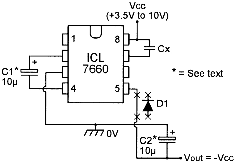
FIGURE 17. Method of reducing oscillator frequency.
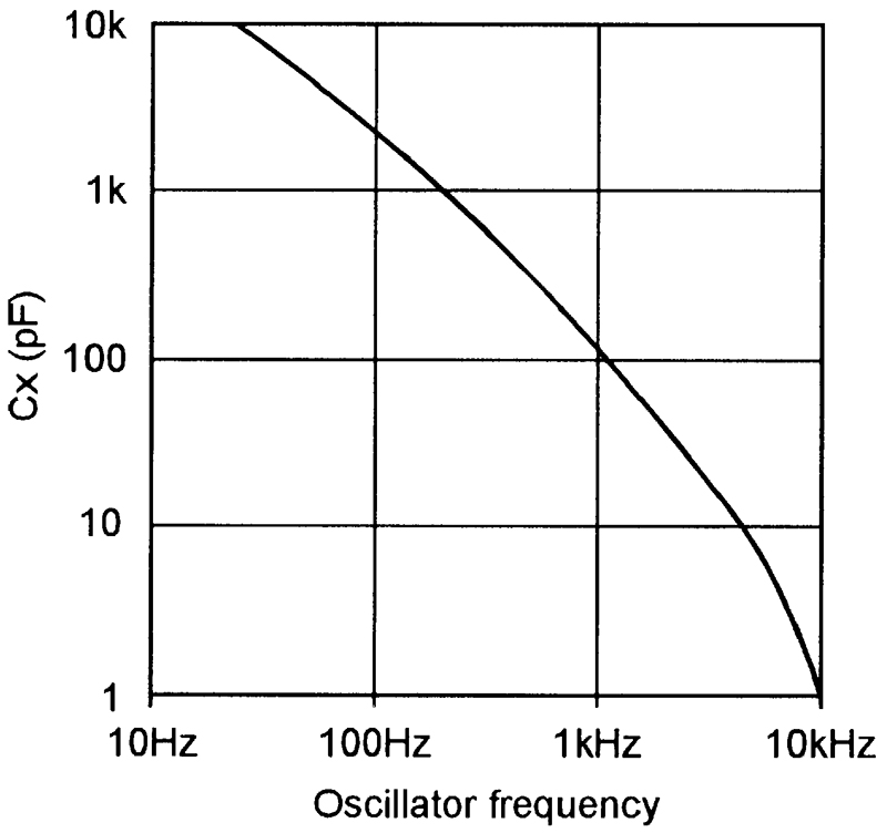
FIGURE 18. Cx versus oscillator frequency graph.
Another way of reducing the oscillator frequency is to use pin 7 to over-drive the oscillator via an external clock, as shown in Figure 19.
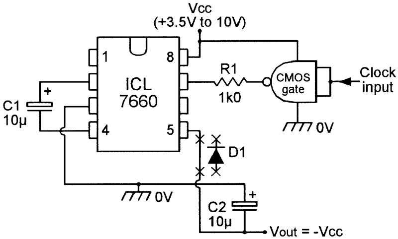
FIGURE 19. External clocking of the ICL7660.
The clock signal must be fed to pin 7 via a 1K0 series resistor (R1), and should switch fully between the two supply rail values; in the diagram, a CMOS gate is wired as an inverting buffer stage, to ensure such switching.
DIODE-STEERED CHARGE PUMP CIRCUITS
So far, this article has described three of the four most widely used types of DC voltage conversion circuit.
The fourth type of converter is sometimes known as a ‘diode-steered charge pump’ circuit, and Figure 20 shows an example of one of these ‘pumps’ used in conjunction with an ICL7660 IC to make a converter that gives a positive output voltage of almost double the original supply voltage value.

FIGURE 20. Diode-steered charge pump type of voltage doubler.
The pump consists of D1-C1-D2-C2, and is driven by the low-impedance squarewave output of pin 2 of the IC. The circuit action is very simple, as follows:
When the pin 2 output of the ICL7660 is switched low, it connects the low end of C1 to the 0V line, so C1 charges to almost the full Vcc value via forward-biased diode D1. When the pin 2 output switches high again, it pulls the low end of C1 up to Vcc, thus driving the top end of C1 up to almost double the Vcc value, thus reverse-biasing D1 and forward-biasing D2, and forcing C1 to dump its excess charge into C2, which thus charges up to almost double the Vcc value.
This process repeats continuously, with C1 automatically replacing any charge currents that are withdrawn from C2 by external loading circuitry. In practice, diodes D1 and D2 reduce the available output voltage by an amount equal to their combined forward volt drops, so they should ideally be low-loss germanium or Schottky types.
This ‘charge pump’ type of circuit is far more powerful than a conventional capacitor-diode voltage-doubler circuit, and can easily supply 10s of milliamps of output current.
Finally, to complete this look at DC voltage converter circuits, Figures 21 to 23 show three useful variants of the basic ‘charge pump’ circuit.
Figure 21 shows how the charge pump circuit of Figure 20 can be combined with the standard ICL7660 negative-voltage generator circuit of Figure 13 or 14 to make a combined positive voltage multiplier and negative voltage converter that provides dual output voltage rails from a single-ended input supply.
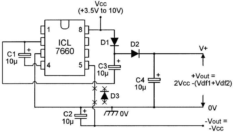
FIGURE 21. Combined +ve voltage doubler and -ve voltage converter.
Figure 22 shows how two of the Figure 20 type diode-steered charge pumps can be cascaded to make a voltage trebler that gives a positive output voltage that has an unloaded value equal to three times the Vcc voltage, minus the value of the series-connected diode volt drops. Typically, the circuit gives an output of about 27V when powered from a 10V supply.
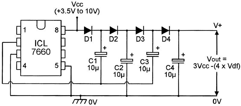
FIGURE 22. Charge pump type of voltage trebler.
Additional D3-C3-D4-C4 stages can be cascaded by wiring the low end of each odd-numbered capacitor to pin 2 of the IC, and the low end of each even-numbered capacitor to the 0V line; each new stage increases the available output voltage by Vcc minus two diode volt drops.
Finally, Figure 23 shows a diode-steered charge pump negative-voltage generator circuit, in which diode and capacitor polarities are simply reversed and referenced to the 0V line.
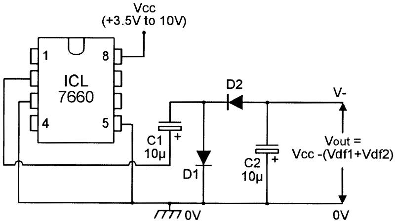
FIGURE 23. Diode-steered charge pump negative-voltage generator.
This circuit (when using ordinary silicon diodes) gives a typical unloaded output voltage of only -8.8V when powered from a 10V supply, but gives far better voltage regulation than a conventional ICL7660 negative voltage generator circuit. NV