Recap
In our last episode, we got a little shifty and learned about the 74HC595 and 74HC597 shift registers, wrote some software SPI (Serial Peripheral Interface) code, and built a new and improved (twice the eyes!) Cylon Eyes project. All that was in preparation for learning about hardware SPI so that we can use it to communicate with external Flash EEPROM memory. So now, we're ready to create a library with hardware SPI functions. We will use the library with the built-in 4-Mbit DataFlash on the Atmel AVR Butterfly shown in Figure 1.
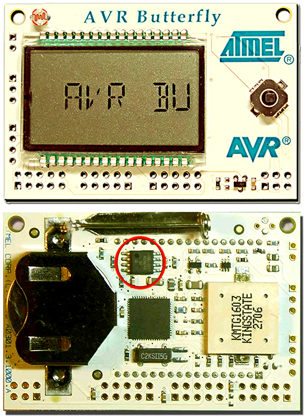
FIGURE 1. Four-Mbit DataFlash on Atmel AVR Butterfly.
The hardware used for the demonstration and the AVR Butterfly are available in the C Programming Book and Projects Kit combination that you can get from the Nuts & Volts webstore.
AVR SPI Library
This time, we will create, document, and share a library of some AVR software and hardware SPI functions. To help keep things simple, we will only look at the SPI master mode — but the general principles apply to both master and slave modes so if you need your AVR to be a slave, you should be able to figure out how to implement this from the supplied code.
In Workshop 28, we learned how to bit-bang (you control each pin state) a software SPI bus so that we could theoretically use any available AVR 4 I/O pins to create an SPI link. We wrote the code to simplify the process of creating multiple SPI links and for compiling the code for multiple AVR devices (ATmega169, ‘328, ‘644). Now, let's extend that code and put it into a library of source code modules.
With software SPI, we are only limited in number of SPI devices by the number of available I/O pins. However, with the hardware SPI we have only a single SPI – but it requires that we generate our own slave select line, thus allowing us to have many slaves as shown in Figure 2.
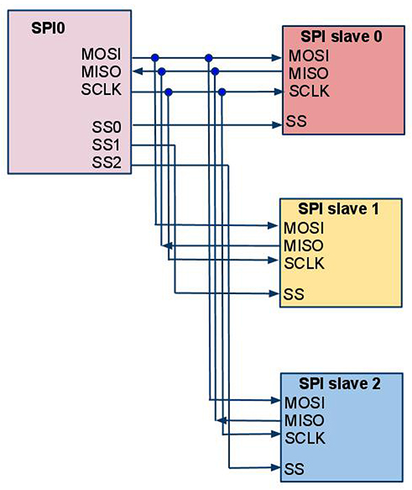
FIGURE 2. Multiple slaves.
The slaves will only pay attention if their SS pin is held low, so by simply holding the other slave SS lines high, we get them to ignore us. We can also expand the number of slaves by daisy-chaining them as shown in Figure 3.
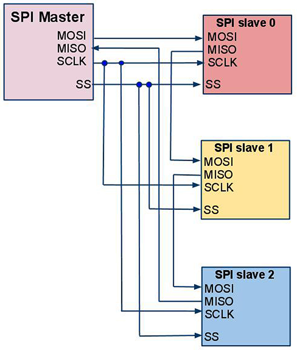
FIGURE 3. Daisy-chained slaves.
The difference in using these two is that for the first, we have to select only one device at a time; in the second, we select all the devices at once, but must transfer all the data for each device at once (in the case shown, it would be three bytes).
Hardware SPI
Even after all these years, I still cringe when I open the datasheets for a device. Atmel does as good a job as any, but it is still a daunting task to figure out among all the choices given, what subset to select for use in my particular application. SPI is one of the simplest peripherals that you can imagine, but look at the datasheet for any of the ATmegas we will use and skim the SPI section. Good grief! Lucky for you, though, I’ve selected a nice little subset that works well with the shift registers we looked at last time, and the DataFlash that is resident on the Butterfly.
Let me insert a special note here: The hardware slave select line /SS is not controlled by the hardware SPI, but must be controlled by the user. This confused me for a minute since it really doesn’t make sense that they designate a /SS line when you can actually use any I/O line for /SS.
But then it does make sense because if you are using the hardware SPI in slave mode, then you must use the designated /SS line. We won’t be doing the slave mode but at least now you know why it is provided.
One Size Fits All — Yeah, Right ...
In order to make the library flexible, we are using some preprocessor commands that let us define items that we want compiled and ignore items we won’t be using. We discussed doing this last time when we showed how we could write code that could be compiled for either the Butterfly, the Arduino, or the BeAVR40 by simply removing the comment ‘//’ directive from a line:
#define Butterfly<br />
//#define Arduino<br />
//#define BeAVR40
Later in the code:
#if defined (BeAVR40)<br />
    // This section will be compiled only if<br />
    // BeAVR40 is defined<br />
#elif defined (Arduino)<br />
    // This section will be compiled only if<br />
    // Ardino is defined<br />
#elif defined (Butterfly)<br />
    // This section will be compiled only if<br />
    // Butterfly is defined<br />
#else<br />
    // This line prints as an error if you<br />
    // forget to define a board<br />
    #error “No board defined”<br />
#endif
While this is a very handy concept, it does tend to junk up the appearance of the code and make it harder to read. For our SPI library, we will allow the user to define multiple numbered SPI links such as SPI0, SPI1, … SPIx. For each of these links, the user can define it as either software or hardware by defining either SPI_SOFT or SPI_HARD. I’ve written and tested the code for SPIO for both SPI_SOFT and SPI_HARD modes. If the user wants additional SPI links, then it is a ‘simple’ matter of copying the SPI0 code and changing the 0 to whatever number is desired, then going through and carefully assigning new I/O pins if you are using the software version or new hardware SPI pins if hardware. When you look at the code, it might take a few moments to figure out what I’m doing with all the defines, but bear with this since it will help create some very useful software concepts for making code easier to use with more than one device.
Setting Up the SPI Registers
For similar reasons, we will use aliases for register and port names that vary between devices. For instance, the slave select data direction register is DDB4 for the Butterfly (ATmega169); DDB2 for the Arduino (ATmega328); and DDB6 for the BeAVR40 (ATmega644). By using the gcc compiler preprocessor, we can let it decide which one of these registers to use by using the #define preprocessor directive to define the device, then let the compiler select from the list of #ifdef – if defined – so that it uses the correct register for the device we are using. You can see all the SPI registers for each device in the source code in Workshop29.zip available from Nuts & Volts. Since we are using the Butterfly in this example, the registers are:
#if defined (Butterfly)<br />
#define MOSI_HARDWARE_PIN PORTB2<br />
#define MOSI_HARDWARE_DDR DDB2<br />
#define MISO_HARDWARE_PIN PORTB3<br />
#define MISO_HARDWARE_DDR DDB3<br />
#define SCLK_HARDWARE_PIN PORTB1<br />
#define SCLK_HARDWARE_DDR DDB1<br />
#define SS_HARDWARE_PORT PORTB<br />
#define SS_HARDWARE_PIN PORTB4<br />
#define SS_HARDWARE_DDR DDB4
If we had hardwired (used the register name instead of the defined alias) these registers in the software, then if we built it first for the Butterfly and later wanted to port it to the Arduino board we’d have to hunt down every place where each of the nine registers differ and change it. The SPI is about the simplest peripheral on an AVR so, again, this ‘one size fits all’ technique becomes even more important for creating libraries that you want to use with more than one AVR device.
An example of this usage is shown next in the spi0_hard_init_master() function. Since we have gone to the trouble of providing aliases such as MISO_HARDWARE_PIN, we only have to change from Butterfly to Arduino one place in the header to convert the function from working on the Butterfly to the Arduino.
void spi0_hard_init_master(void)<br />
{<br />
    PORTB |= (1<< MISO_HARDWARE_PIN) \<br />
             | (1<< MOSI_HARDWARE_PIN) \<br />
             | (1<< SCLK_HARDWARE_PIN) \<br />
             | (1<< SS_HARDWARE_PIN);
    //Set MOSI, SCK AND SS to outputs<br />
    DDRB |= (1<< MOSI_HARDWARE_DDR) \<br />
            | (1<< SCLK_HARDWARE_DDR) \<br />
            | (1<< SS_HARDWARE_DDR);
    // Set Miso to input<br />
    DDRB &= ~(1<<MISO_HARDWARE_DDR);
    // SPE - SPI Enable<br />
    // MSTR – Master\Slave Select<br />
    // SPRO - Fosc/16<br />
    SPCR = ( 1 << SPE ) | ( 1 << MSTR ) | ( 1 << SPR0 );<br />
}
SPCR — SPI Control Register
There are also too many choices for the SPCR register. You’ll have to carefully read the datasheet if you want your SPI to be different from this one. In our case, we chose to set the bits as follows:
- SPE – SPI Enable: A write to 1 enables the SPI.
- MSTR – Master/Slave Select: A write to 1 selects the master mode.
- SPR0: The clock bits default to 0 so setting this bit to 1 selects an SCLK rate of 1/16 the AVR oscillator speed. In our case, 16000000/16 = 1 MHz.
We just leave the other SPI control bits at their default 0 state which selects for the desired options.
Using Our SPI Library
Using the SPI couldn’t be simpler (or rather, I couldn’t make it simpler). First, you select the device you are writing to by setting its slave select (/SS) pin low, then load the data you want to send into the SPDR (SPI Data Register), then wait for the SPIF flag in the SPSR to be set. Then, finally load the data received from the SPDR register. (Note that the data goes out of and into the same register — as shown in Figure 4.)
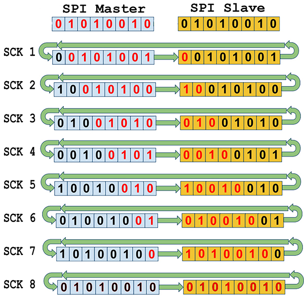
FIGURE 4. SPI shift.
This is shown in the spi_hard_master_rw8 function below:
// Simultaneously sends a byte to the slave<br />
// and receives a byte from the slave<br />
uint8_t spi0_hard_master_rw8(uint8_t to_slave)<br />
{<br />
    uint8_t from_slave;
    // select slave<br />
    spi_hard_set_ss();
    // Put byte in SPI data register<br />
    SPDR = to_slave;
    // Poll SPIF-flag until transfer complete    <br />
    while(!(SPSR & (1<<SPIF)));
    // Get the SPI data reg.<br />
    from_slave = SPDR;
    // deselect slave<br />
    spi_hard_clear_ss();<br />
                            <br />
    //return it<br />
    return from_slave;<br />
                            <br />
}
Rather than go into a lot more detail about the SPI source code, I invite the reader to look at the two applications in this episode’s Workshop29.zip: one for Chaser Lights and one for testing the DataFlash.
Atmel DataFlash
Figure 5 is a block diagram of our DataFlash. The Atmel DataFlash family has from 1 to 128 Mbit (500 Kbyte to 16 Mbyte) SPI serial memory ICs that come in small packages and require only four pins for access. They use on-board SRAM, small page sizes, and flexible opcodes to facilitate data access. Atmel claims this is the ‘world’s number one selling serial interface Flash family’ and that they make the ‘world’s fastest serial Flash’ (go to www.Atmel.com for more exciting marketing hyperbole).
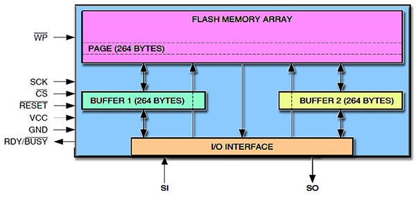
FIGURE 5. DataFlash block diagram.
With 100K guaranteed write cycles, it is unlikely that we are going to wear out the Butterfly DataFlash, but please note that for serious — as in commercial — use of the Atmel DataFlash you should carefully read the datasheets and get the Atmel DataFlash Sofware Suite (you have to ask them for it from Atmel) to increase a device’s life span. Also, to keep from killing it immediately it is important to remember that on the AVR Butterfly the DataFlash is restricted to 2.7 to 3.6 volts, but the ATmega169 is rated up to 5.5 volts. So some folks use a five-volt supply and then fry their DataFlash. This kind of error is called: ‘You din’a RTFM!’
The AT45DB041B has 26 opcode commands that control its actions. These commands provide a variety of functions but as usual we will only look at a useful subset of the myriad of possibilities. We will learn how to read the device status, read and write data to the 264-byte SRAM buffers, tell it to write a buffer to a Flash page, and tell it to read a Flash page into a buffer.
Talking to DataFlash
Much of the DataFlash low level software was adapted from the Martin Thomas gcc port of the original Butterfly software available at www.siwawi.arubi.uni-kl.de/avr_projects/. However, a lot has been changed to fit into my evolving coding style and we will use our SPI library.
Read the Status Register
The simplest thing we can do is read the DataFlash Status register. This is a relatively straightforward use of SPI. We send the opcode 0x57 for ‘read the status register’ to the DataFlash; then we send a dummy byte while reading the byte returned which is the status byte.

FIGURE 6. The DataFlash status register.
Figure 6 shows the bits in the status register. Bit 7: RDY/BUSY reads 1 if the device is ready to write a buffer page to a Flash page and 0 if it is busy. Bit 6: COMP is for the most recent Main Memory Page to Buffer Compare operation; it is 0 if they are the same and 1 if there is any difference. Bits 5–2 provide device memory size information. The lowest two bits aren’t used.
Our df_read_status function reads the status register and uses the device information bits with a lookup table to determine the value of the df_page_bits and df_page_size variables that may be used in other functions.
uint8_t df_read_status (void)<br />
{<br />
    uint8_t result,index_copy;<br />
    <br />
    // Toggle SS to reset DataFlash command<br />
    // decoder<br />
    spi0_hard_SS();<br />
    <br />
    // Send opcode to read the status<br />
    // register<br />
    result = spi0_master_rw8(StatusReg);<br />
    // Send a dummy byte to receive the<br />
    // results<br />
    result = spi0_master_rw8(0x00);<br />
    <br />
    // Get the size information<br />
    index_copy = ((result & 0x38) >> 3);
    // Get the number of page address bits<br />
    // from the lookup table<br />
    df_page_bits = pgm_read_byte(&df_<br />
    page_bits_array[index_copy]);<br />
    // Get the size of the page (in bytes)<br />
    df_page_size = pgm_read_word(&df_<br />
    page_size_array[index_copy]);
    // Return the status register value<br />
    return result;<br />
}
Test Read/Write Status Register and SRAM Buffers
For our first test, we will read the status register and show the bits in the status register, along with the value of the page bits and size variables.
void show_status()<br />
{<br />
      char status = 0;<br />
    char array[] = {0,0,0,0,0,0,0,0,0,0,0};<br />
    <br />
    // Get the status<br />
    status = df_read_status();
    uart_send_string(“\rStatus:\r”);<br />
    show_bits(status);
    uart_send_string(“\rdf_page_bits: “);<br />
    itoa((int16_t)df_page_bits,array,10);<br />
    uart_send_string(array);<br />
    uart_send_string(“\rdf_page_size: “);<br />
    itoa((int16_t)df_page_size,array,10);<br />
    uart_send_string(array);<br />
    uart_send_byte(‘\r’);<br />
}
The show_status() function sends out the following on our serial port:
Status:<br />
10011100<br />
>—————<<br />
df_page_bits: 9<br />
df_page_size: 264
This tells us that since bit 7 is 1, the device is not busy, that it has nine page bits, and that each page is 264 bytes.
For testing the buffer read\writes, we use the DataFlash library functions df_buffer_write_string and df_buffer_read_string. These two functions are very similar so we will show only the write function.
The parameters are:
df_buffer_no - Select buffer 1 or 2.
df_int_page_adr - Selects Flash page address.
No_of_bytes – Sets number of bytes to be written.
*BufferPtr - Provides the address of the buffer for copy of bytes.
df_buffer_write_str (uint8_t df_buffer_no, \<br />
uint16_t df_int_page_adr, \<br />
uint16_t No_of_bytes, \<br />
uint8_t *BufferPtr)<br />
{<br />
    uint16_t i;
    // Toggle slave select<br />
    spi0_hard_SS();<br />
    <br />
    // Write to buffer 1<br />
    if (1 == df_buffer_no) //write byte(s)<br />
    to buffer 1<br />
    {<br />
        // Send buffer 1 opcode<br />
        spi0_master_rw8(Buf1Write);<br />
    }<br />
    else if (2 == df_buffer_no)// Write to<br />
    Buffer 2    <br />
    {<br />
        // Send buffer 2 opcode<br />
        spi0_master_rw8(Buf2Write);<br />
    }
    //Send dummy<br />
    spi0_master_rw8(0x00);<br />
    // Send upper part of buffer address<br />
    spi0_master_rw8((uint8_t)<br />
    (df_int_page_adr>>8));<br />
    // Send lower part of buffer address<br />
    spi0_master_rw8((uint8_t)<br />
    (df_int_page_adr));<br />
        <br />
    for( i=0; i<No_of_bytes; i++)<br />
    {<br />
        // Write byte pointed at by<br />
        // *BufferPtr<br />
        spi0_master_rw8(*(BufferPtr));<br />
        // Point to next byte<br />
        BufferPtr++;        <br />
    }<br />
}
We test the buffer read\write with the buffer_test() function by using two arrays: one with “Hello, World!” and the other with “Goodbye ya’ll.” We first verify that these arrays show what they are supposed to, then we write the first array to buffer 1, read buffer 1 into the second array, and show them again to verify that the first array was sent to the buffer and then read back into the second array. Since we are running short on space we’ll just show the results of these tests in Figure 7.
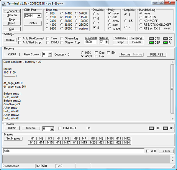
FIGURE 7. Output on Bray’s Terminal.
The code we’ve shown here should be enough to introduce the principles we used to create both the SPI hardware and the DataFlash libraries. We test these libraries in the DataFlashTest project in Workshop29.zip. We will use these libraries next time to create a Butterfly Data Logger. NV
Corrections
The Figure 2 diagram that appeared in the PRINT edition of Nuts & Volts was incorrect. The web version that is shown here has the correct diagram.