Why would I want to concentrate on designing a circuit board that's a piece of cake to build? Isn’t that for the manufacturer to worry about? When they have a list of things to do, they just make the next board in line, right? Well, yes and no. You see, there are small behind-the-scenes decisions made every day. Some boards are put at the top of the “to do” list and some are put at the bottom. Even if you aren’t making a microwave communications array for NASA’s next exploratory rover, someone else is. While your board might not cause problems in the shop, you still want to make sure your project stays on schedule while there's a redo on someone else’s.
In this article, I’ll talk about a typical two-sided board and some of the things you can do to make it easier to manufacture. Some like to call it DFM — Designed For Manufacturing. I like to call it designing a “big, dumb board:” big holes, big traces, big pads — any "dummy" could make it. While I won’t be discussing any specifics about a multi-layer board (they already have a complex design by default), many of the same principles apply.
When reading the design rules specified by your manufacturer, remember that these are the maximums, not guides. Just as you wouldn’t test the 60-0 MPH stop time on your car at every light, don’t push the manufacturer to the limit with your design if you don’t have to.
You have direct control over three steps of the circuit board making process:
- Drilling
- Imaging
- Screening
In drilling, we’ll discuss just that — drilling — more specifically, hole sizes. Imaging will include resist imaging, plating, and etching. Screening is the white character screen that makes your board look so professional.
Drilling
Drilling is pretty self-explanatory. You are poking holes in copper. What many people probably don’t know is just what the capabilities and limitations are regarding typical circuit board drills. The drill spindles are very unique and come in two basic styles: ball bearing and air bearing. The type that your manufacturer has won’t matter to you. Simply understand that these spindles have high end speed ranges. Their lowest speed is either 14K or 20K RPM — depending on whether they are air bearing or ball bearing — and the upper range is from 80K to 120K. To put that into perspective, your car’s engine probably red lines at about 6,000 rpm.
Don’t specify too small or too large of a hole.
To drill a .250” hole, the ideal speed would need to be about 7,500 rpm. This is not possible, so the minimum speed is set and drill bits dull fast. Large bits are good for about 1/4 the number of holes as smaller sizes. At the other end of the scale, you probably don’t want to specify a hole that is smaller than about .028” or so. Holes as small as .001” are possible in some of the more advanced shops, but .028” seems to be a “magic” number. Any smaller than this and anything that can go wrong, will. Namely, small bits break more often — much more often. Specifying a .008 inch hole is a sure fire way to slow things down. Try to keep component hole sizes in the .030’s and .040’s and mounting holes around .125”. Most manufacturers would probably prefer to keep the hole size .250” or less.
Don’t make 14 different hole sizes.
While we are talking about holes, you are the one who specifies the hole sizes. Many cad/cam programs will output a drill file that you might send to the manufacturer without even looking at it and the hole sizes are included in that file. It can be large and intimidating, but it is really quite simple. It is a text file and, basically, the header gives the drill sizes. Following that is the X,Y coordinate of each hole. By looking at the header, you can see how many different hole sizes there are and what they are.
If you see many hole sizes that are similar (.034, .036, .039), consolidate them into the larger hole size. If you are worried about accuracy, remember that the manufacturer will “bump” this size up .005” or .006” anyway to account for the plating that occurs inside the hole. Since plating varies across the panel, so will the hole sizes (by .001” or so). If you don’t feel comfortable manipulating your drill file yourself, tell your manufacturer it is okay for them to do it.
Imaging
Your standard two-sided circuit board will go through many standard steps during its construction. After drilling, the holes will be deposited or coated with a small amount of copper. Then they will be imaged. After that, they will be plated, building the traces up and making the copper in the holes thicker. Next, they are etched, removing the excess copper and leaving your traces. Then they will have the solder mask (green) and character (white labeling) silk screened on. Finally, they go to routing and the individual boards are cut out of the panel. There are some more steps and this is simplified, but this gives us a good base of understanding.
Don’t specify too small of a trace.
The entire imaging and plating area is a group of two- and three-dimensional processes that come together to make a product that was designed with two dimensions in mind. To a cad program, that trace is a line that is X-number of inches wide. To a circuit board manufacturer, that is a trace that has to be built up and etched away. It has to be made tall enough and has to start out wide enough to account for etch back and light undercutting. It has to be built to the specified height in plating. Also, the ratio of how wide it is to how tall it is must be enough to withstand all of the variations that can come into play.
The first part of creating the traces is the actual imaging process. First, the board is laminated with a photo sensitive film. A two dimensional photo image is laid on the board and the image is exposed onto the film. The film is then developed, essentially washing away what will be the circuit and leaving “grooves” to be plated up. This is the first three-dimensional process that can create a headache with a thin line. If any light creeps under the edge of the photo, it will reduce the size of the trace. If the trace is thin to begin with, it may disappear all together. The developed image must be a three-dimensional “canyon” that has straight walls and matches the photo in size and shape when viewed from the top.
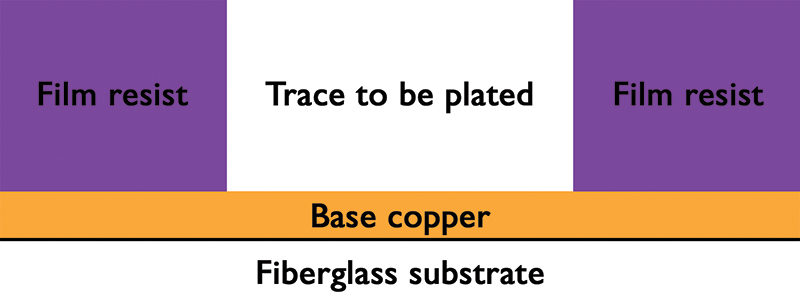
Illustration showing cross section of film after developing.
These grooves are deep. They are so deep that you can actually run your finger across the board and feel the image. This is no accident. The boards are going to go through some harsh environments and you want your plating resist to survive. The resist also has to be thicker than — or at least as thick as — the plating will be. It is going to be the “mold” that contains and shapes the electrical plating.
After imaging, the boards are electrically plated. The little canyons are filled with copper during the plating process. The holes also get plated at the same time, making them strong enough to withstand stuffing a component into them, melting solder into it, and even removing a component, if necessary. On top of the copper, an etch resist is plated — either tin or tin/lead, depending on the shop and what kind of finish the board will have. After that, the film is stripped off and it is on to etching.
Etching is another three-dimensional process necessary to produce a two-dimensional result. Not only does the copper around a trace get etched away, but so does the side of a trace. While a trace may only be .002” tall, it can easily lose as much as .002” off both sides at its base. That means that, if you had a trace that was only .004” wide, the base could be completely etched away and the trace would physically lift from the panel.
Thin traces take special handling and special handling can drop you a couple of notches on the “to do” list. Consider keeping your trace size to a minimum of .010”. If you have the room, .030” is a no-brainer for the shop. A .030” trace will survive if every process in the shop has a problem. A .010” trace will survive as long as everything does what it is supposed to. A .005” trace will only survive if everything goes just right. Smaller traces can be done if necessary, but that hardly qualifies as big or dumb.
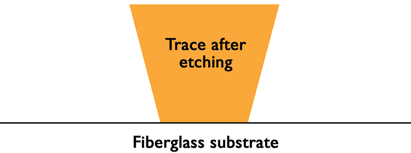
Illustration showing cross section of trace after etching.
Make sure your pad is big enough.
The same photo process that made the traces will also make the pads at the same time. The pads are what will actually be used to line up the board. If you get a board that is aligned off to one side, many people would say the holes were drilled wrong when, in actuality, it was the pads and traces that were put in the wrong place.
The film stretches and shrinks with changes in heat and humidity. If you specify a pad size that is .012” bigger than the hole, that is a small pad. If the manufacturer steps the hole size up .006”, you now have .006” left over. That is a .003” annular ring — the space between the edge of the hole and the edge of the pad. If the drill was off by as little as .001” and the film stretched by as little as .002” across an 18” section, you would suddenly not have any pad left along one side of a hole. That is called “breakout” and it happens enough with close-tolerance boards that there is a specification as to how much is allowed.
Make sure your pads are .035” bigger than the holes. That may sound like a lot, but remember that the hole size will be stepped up .005” to .006”. Subtract the hole size from the pad size, remove the .005” that was stepped up, divide by two to get the annular ring size, and you will be left with a .015” annular ring. Grab a pair of calipers and take a look at what .015” looks like. It isn’t a lot.
If your board has through-plated holes, make sure they are all plated through.
Sometimes, someone will only need some of their holes plated through and that is fine. Where it runs into trouble, though, is when you have holes that aren’t plated through and have a pad on the bottom side for a component without a matching pad on the top side. Light travels down from the top of the board when it is exposed with the circuit. It goes through the hole without a pad and hits the back side of the pad on the bottom of the board. That makes a “dot” the size of the hole that will literally float around in developing.
These “dots” like to land back on the board and attach themselves where there should be a continuous trace. That means there is no plating and a break in the trace. Again, this is a problem that is usually found late in the process — well after it is too late to fix it — and another redo is needed.
Through–plated holes make soldering easier. The solder will “wick” from the bottom side to the top and you will get a stronger connection. You can tell at a glance if you have a good solder joint by looking at the top of the board. Your board will have a truly professional look. It is one of those things that you can’t put your finger on, but it makes one project look better than another. In addition, your board will be easier to manufacture and you have a better chance of getting it on time. Just simply place a pad on top every place you have a pad on the bottom and the holes will be plated-through.
Check your design for errors (opens).
Make sure you zoom in and zoom out on your design while giving it the final once-over. While a space or clearance might look good on the screen, it can be impractical in real life. Keep your spaces to .010” or more and be realistic about physical limitations. I have seen where someone placed mounting holes .010” away from the edge of the board. It looked good on the screen until you zoomed out. When you looked at the board actual size, the .010” couldn’t be accurately displayed on the screen. If this sliver of material had survived, it would have been brittle and flimsy, not good for a mounting hole. While you are at it, print your circuit out on paper. If your printer is having trouble accurately displaying the image, your job probably won’t be classified as a piece of cake.
While routing your traces, make sure you have the “snap to” function turned on. This will ensure that all of your traces actually terminate into pads and that two joining traces actually connect together. Sometimes, if you zoom in to a pair of traces, you will see where they don’t actually connect. The same thing happens where a trace meets a pad. If you don’t catch it before the film is printed, it might not be caught before the board is being manufactured. All too often, these errors are caught in Quality Control, the last step before a board is sent out. That means a redo and a long wait on a board that should have been done already.
Be realistic about your silk screen characters.
One last area that seems to be often overlooked and consistently specified incorrectly is the character silk screen. The process that you might have used to make T-shirts in art class back at summer camp is almost the same process that is used to put the white labeling (the character screen) on your board. First, a film is exposed and developed with the image of your characters. Next, it is fixed to the silk screen. Then, a squeegee is used to push ink through the screen and film and onto your board. If the size of the opening is too small, the ink will dry in the screen and won’t go through. It doesn’t take long — only a few seconds. If you have ever gotten a board with skips in the character, that is what happened.
You will want to specify an aperture width of .010” to .012”. That means that, while your characters will possibly survive if they are as little as .040” or .050”, you will probably want them to be .070” tall or taller. When you print your circuit, play around with a pair of calipers and see how tall you can make the characters and still have the board look good.
Illustration showing 5 mil annular ring, 10 mil traces, and 40 mil character.
In Conclusion
You have direct control over your design and, therefore, you are responsible for how easy your board is to build. Many times, what could be a “big, dumb board” is turned into a “nightmare board” just because it is ill–designed. Follow these rules and your board should be a piece of cake to build:
- Keep your hole sizes in the .030” to .040” range. Keep mounting holes .250” or less.
- Specify six or fewer hole sizes.
- Make your traces at least .030” if possible.
- Make your pads at least .035” bigger than the hole size.
- If some holes are plated-through, they all should be plated–through.
- Make your silk screen characters .070” tall or taller.
- Print your circuit on paper and see what it actually looks like.
If you have some tolerances that are tighter than others, let your shop know. If they know that a board is just there to connect electricity, instead of a microwave board with onboard capacitors, they can widen traces and increase pad size as necessary. If you can, arrange to take a tour of your circuit printing shop. I guarantee that you will be surprised as to what actually happens during the manufacture of a circuit board. NV