Before solid-state electronics, vacuum tubes were used for everything — from high volume consumer radios and televisions to exotic one-of-a kind military and scientific applications. A lot of the old and interesting glass is still around to be found at hamfests, estate sales, and online auction sites. It’s fun to collect and experiment with forgotten technology! But, you’ll need a stable high voltage power supply to get started.
Safety Warning!
Anyone attempting to construct and use this module should be aware of high voltage safety. Although the energy is limited, there are high voltages on the PCB, components, and connectors. Capacitors may store some energy after the power is removed. Remember, high voltage circuits bite fools!
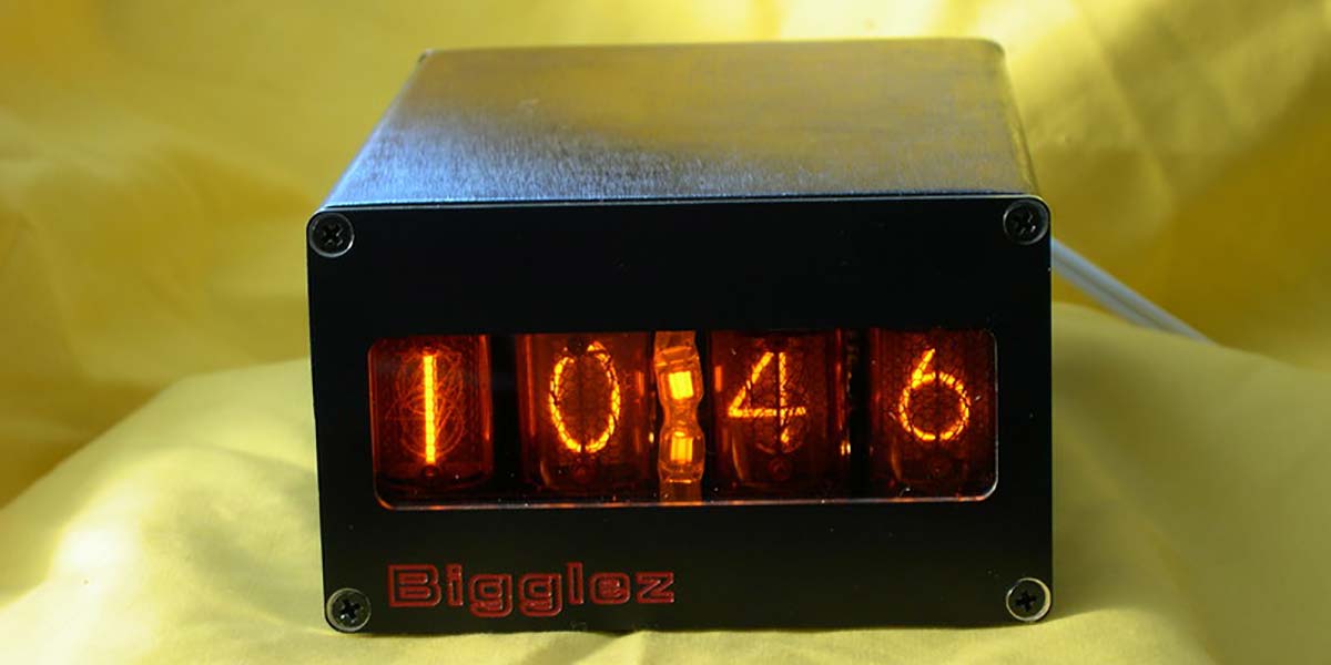
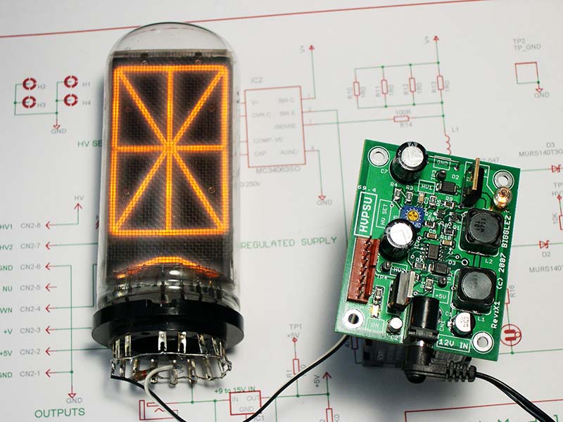
I needed a couple of hundred volts to operate some Nixie tubes (see the sidebar to find out why), so I created a circuit. The prototype was so handy that I reworked it into a self-contained high voltage power supply unit (HVPSU) that I’m presenting here (Figure 1).
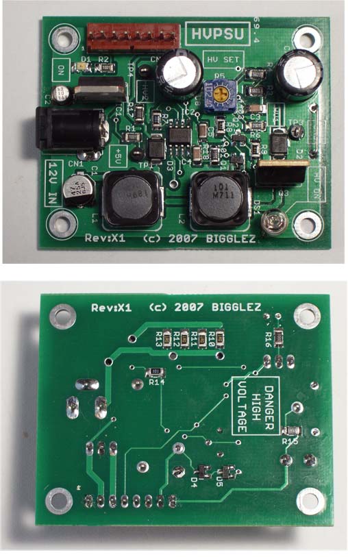
FIGURE 1. Photo of completed module.
The HVPSU can be built into other projects as a module with a 0.1 inch grid and 0.1 inch pitch header, and can be connected with a wiring harness or mounted directly on perfboard for those projects not ready for a PCB (printed circuit board) commitment. The DC power jack mates with a wall-wart brick, and an LED power on and neon high voltage active indicators complete the design. Table 1 is the target specification and Table 2 shows the performance measured.
Physical Size:
Double sided PCB 63 mm (2.5”) x 51 mm (2.0”) x 23 mm (0.88”)
Input:
12V DC nominal (10V to 15V).
Outputs:
HV1: Regulated 175V to 200V DC, 0 to 15 mA.
HV2: Unregulated (zener clamped) 60V DC nominal, 0 to 5 mA.
LV1: Pass through of DC input voltage (aids in wiring or piggy-back assembly).
LV2: Regulated 5.0V ±5% DC, 0 to 100 mA.
Control Input: (optional)
TTL (0-5V) compatible HV shutdown: Used to turn off HV and save tubes, while keeping 5V and the DC pass through active. Defaults to HV on, connect to 5-15V to shut down.
Indicators:
DC Input: LED (Yellow).
HV Output: NE2 Neon.
Adjustments:
HV Set single turn potentiometer. Covers approx. 175-200V.
Mounting:
Four 3.3 mm (0.130” #4 clearance) mounting holes.
Connector: Molex KK-100 header eight-position header.
Output Limits:
Maximum current in regulation: 15 mA (enough for six medium to large tubes).
TABLE 1. Specifications.
| V In |
I In |
P In |
V Out |
R load |
I load |
P Out |
Eff |
| 13.3 |
280 mA |
3.72W |
184V |
15,520 |
11.86 mA |
2.18W |
58% |
| 12.2 |
416 mA |
5.12W |
212V |
15,520 |
13.66 mA |
2.89W |
56% |
Using Digi-Key T983-P5P-ND DC supply or equivalent.
TABLE 2. Measured performances.
Circuit Description
Look at Figure 2.
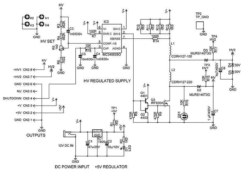
FIGURE 2.
To better understand the operation of the flyback circuit, see the sidebar on Flyback Theory of Operation.
The low voltage section provides a 5V DC output from a linear regulator, IC1. LED, D1 is a power on indicator fed from the 5V supply via R2. IC1 — a TO-220 type — does not require a heatsink for power dissipation of one watt or less. With a 12V DC, input we are limited to 140 mA, and the spec was arbitrarily set for 100 mA max (IC1 dissipates about 700 mW).
The project uses a mix of through-hole (TH) power components and SMT to conserve PCB space, but I discovered (the hard way!) that test probes can be a hazard. To reduce the likelihood of shorting out power circuits with a careless slip of the probe, the test points are isolated with resistors (1K for low voltages and 10K for high voltages). TP1 monitors the 5V DC output.
DC input power is from a 2.1 mm coaxial jack, CN1, which mates to several commercially-made brick power supplies. All other connections are made through CN2, which can be a locking header (on the component side of the PCB) to mate with a wiring harness or an SIP header (on the solder side of the PCB) to allow the module to be piggy-backed on another PCB, a 0.1 inch perfboard, or a solderless breadboard.
Generating a 200V main output along with a second output of approximately 60V DC requires only one flyback converter stage. This was accomplished by tapping the inductor into “one third and two thirds” sections so that the 60V output can be derived from the tap. A commercial tapped inductor was not found, and homemade ones worked well but are messy, so two readily available inductors are used in series.
In any SMPS design, the components in the basic loop (see sidebar again) are under a lot of stress. Component types were carefully selected for the positions of D2, D3, L1, L2, and Q3 — please do not substitute! Ordinary rectifier diodes can’t be used for the HV outputs; the type specified is a fast recovery diode.
Most of the work is done by a DC-DC converter control ASSP (Application Specific Standard Product), IC2. The MC34063 has been on the market for a couple of decades and is sourced by several vendors (and costs less that one dollar in hobby quantities!). As the IC was conceived in the days of power bipolar junction transistors — which are current-driven switches — this circuit requires another stage (Q1, Q2, R8, and R9) to drive the gate of a modern voltage driven PMOS FET transistor.
The main output (HV1) is controlled by a feedback loop that monitors the voltage developed on C7 and at TP3 through a resistor divider chain (R3, R4, R5, and R6). By making R5 a single turn potentiometer, the output voltage can be adjusted over a 15% range. C3 is included to improve stability, and the feedback resistor chain uses two resistors (R3, R4) to limit the voltage stress on each resistor (as I have found high value resistors to drift over time under high voltage stress).
Internally, IC2 generates a 1.25V reference, and this is compared to the voltage from the R5 wiper. Increased output demand lowers the voltage on C7 and the voltage at the wiper of R5, causing IC2 to increase the duration of the drive pulses to Q3. With greater energy stored in the inductor, the output rises to equilibrium again. When the output load is reduced, the opposite action occurs. Shorting or overloading the output is detected by the current limit circuit and the output voltage is allowed to safely fall.
Capacitor C4 controls timing of the internal ramp generator in IC2 at about 35 kHz. I discovered that if the voltage on this capacitor is taken slightly higher than normal, the IC will shut down with no risk of damage to it or other components. So, we have a simple way to shut down the HV using a 5V (or greater) signal on CN2 pin 4.
C5 and R16 filter any noise from the control line. When shut down, there is still a DC path through the inductor and diodes to the outputs, so the lowest output voltage is really that of the DC input supply (12V, in this case), which is true of all inductor based flyback designs.
Output from IC2 is applied to Q1 and Q2 to ensure that Q3 switches quickly and cleanly. Failure to turn Q3 on hard when the inductor is charging can lead to overheating in Q3 due to I2R loss in the device. On the other hand, not turning Q3 off quickly can cause additional power loss in Q3. The parasitic capacitance from drain to gate in Q3 can cause the FET to turn on again mid cycle, usually with destruction of the device! Unused energy from the inductor oscillates with stray capacitance and Q3 drain, causing ringing (see Figure 3).
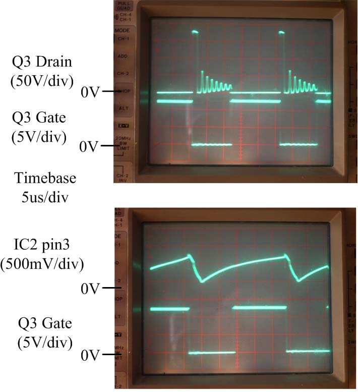
FIGURE 3. Scope waveforms.
Q2 clamps the gate to near ground during the off cycle, and Q1 sources current into the gate capacitance during the on cycle. Q3 lives a hard life with both high voltage stress when off and high current stress when on. This lowers overall circuit efficiency along with core and winding losses in the inductors. Q3 does not require a heatsink, will not get warm at all, and is rated at 5A and 500V.
AC pulses on the drain of Q3 drive a small neon bulb, DS1, via R16, to indicate that high voltage is present. When the module output is unloaded, IC2 will operate in DM (discontinuous mode) and the neon may flicker, which is normal.
The main output (HV1) is from C7, charged through diode D2 and monitored by TP3. The second high voltage output (HV2) is from C8 and TP4, charged by D3 from the inductor ‘tap’ and approximately one third of HV1. It will climb slightly when HV1 is loaded (due to the feedback loop around HV1), so Zener diodes D4 and D5 clamp the HV2 output at 60V nominal (57V to 63V); I used two diodes to spread the dissipation in these tiny SOT23 size parts.
Inductor current is monitored by a low value resistor at the top end and the sawtooth waveform is fed back to IC2 by R14. Because low value SMT resistors are expensive, I used a parallel network of several one ohm 1206 size resistors. Luckily, a partially used reel of “1R0, 1206, Qty 5,000” was found at the local surplus emporium for a couple of dollars and will last me for a lifetime!
PCB Assembly
A PCB is recommended for construction, although I built prototypes on perfboard using mostly TH parts. Layout is not critical but it aids in getting good performance and reliable operation of high voltage circuits. Care is required in directing ground currents around Q3 and the inductors, to keep the high voltage pulses out of the sensitive feedback loop near IC2.
The recommended PCB has both TH and SMT parts; the PCB design files are available in the downloads. SMTs can be hand-soldered, just like the TH parts, and a few components are installed on the ‘solder side,’ so do these first and continue with the other SMTs on the component side next. Leave Q3 off until after initial testing. I’m switching over to SMT parts for hobby projects and discovered that brand new SMT resistors (above 10 ohms) are so cheap that 1% tolerance parts are economical, hence the unfamiliar values on some resistors. The ground test point is fashioned from a piece of tinned copper wire (possibly salvaged from a TH resistor), and makes a great way to hold the mini croc-clips on scope probes.
Power Up Testing
Leave Q3 off the PCB to allow the low voltage regulator to be tested first. If a scope is placed on the Q3 gate pad, a clean square ware drive will confirm that IC2 and related circuits are working correctly. Until Q3 is installed, no high voltage will be generated. Check the 5V output with a DMM (it should be 4.75V to 5.25V).
Install Q3 and check HV1. Adjust R5 over the full range and confirm it covers approximately 175V to 200V. Finally, check HV2 which should be no more than 63V, and typically a little less until the HV1 output is loaded up.
For a regulation check, use a dummy load of 18K 2W on the HV1 output. Or, use a chain of eight 1/4W 18K resistors in series and parallel if high power resistors are not available. Finally, take CN2 pin 4 to 5V and confirm that the HV shuts down. (Remember, photos of the typical scope waveforms are shown in Figure 3.)
Other Uses
The circuit and layout presented here are my “Mark III” design as the two earlier versions paved the way. Areas of interest to me are increasing the switching frequency (from 35 kHz to, say, over 100 kHz) and experimenting with current-mode feedback that should offer better transient load regulation than the voltage mode used by the MC34063 IC. Several modern ASSPs are available for the control loop.
For tube experiments where a heater supply is needed, the 5V regulator (IC1) can be replaced with a 6.0V type, which slightly under runs a standard 6.3V heater at 95%. A heatsink will be required for IC1, and a stronger AC power brick. The output voltage can be changed by using a different value for the pot (R5) and R6, respectively. The main feedback resistor chain (R3, R4) should be kept at approximately one megohm (1,124K with specified components); the upper limit is the breakdown voltage of D2, D3, and Q3, so stick to 250V or lower. Use the following formula to calculate a new output voltage:
Vout = 1.25 * ((R3 + R4 + (R5/2) + R6) / (R6 + (R5/2)))
To calculate a new value for R6 for a given output voltage:
R6 = ((R3 + R4 + (R5/2)) / ((Vout/1.25) + 1)) - (R5/2)
Enter these directly into an Excel spreadsheet to experiment with the center, min, and max range of the trim pot, R5. Or calculate the resistors required for a desired output. The voltage reference in IC2 is good to 2% tolerance. NV
Flyback Theory of Operation
A flyback converter is a member of a family of topologies called Switch Mode Power Supplies (SMPS) that are a variation on a basic circuit consisting of two switches, a magnetic storage component, and an electrical charge storage component. See Figure A. Both switches can be transistors, or more typically, a diode for the second switch (S2), an inductor for the first storage component (L), and a capacitor for the second storage component (C).
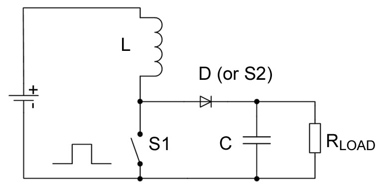
FIGURE A. Flyback model.
When the first switch is closed current from the input voltage is applied to the inductor, as shown in Figure B. Over time, the current in the inductor increases while energy is stored as a magnetic field. After a known time, the first switch opens and the second switch closes, connecting the inductor to the capacitor. The rapidly collapsing magnetic field drives energy from the inductor into the capacitor.
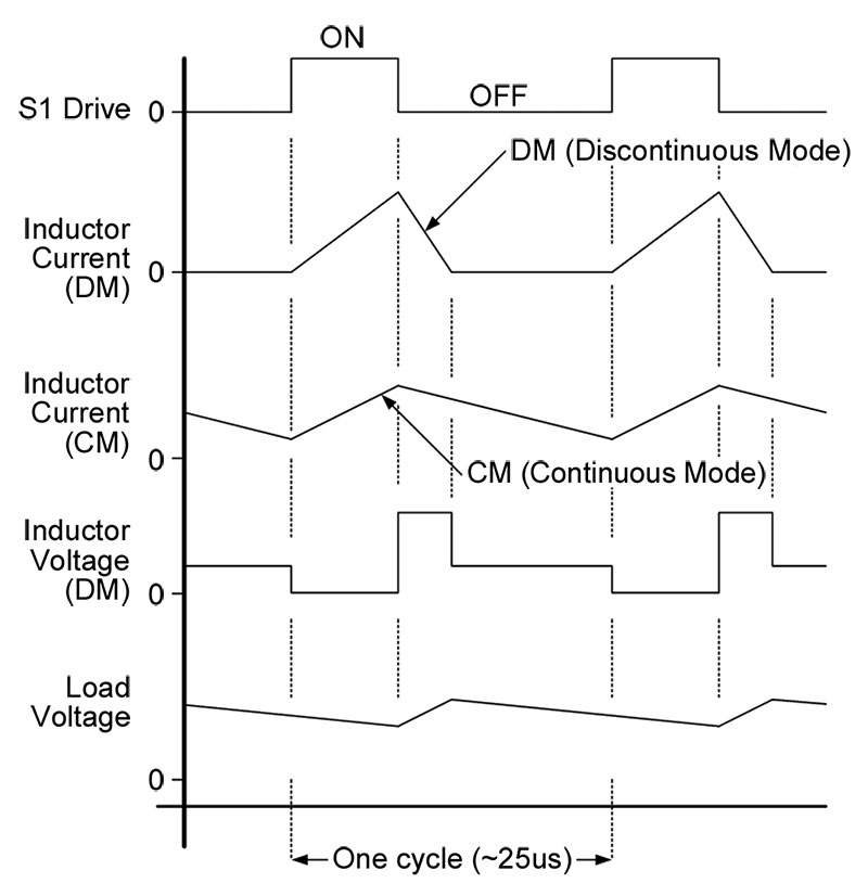
FIGURE B. Flyback waveform diagrams.
The duration for the first switch closure determines the amount of energy transferred. The rapidly collapsing field results in the output being greater than the input voltage, and of opposite polarity. This is therefore a step up topology. Because the common terminal of the inductor is connected to the input supply’s positive side, the resulting output is now more positive than the input.
Another analogy is to consider a water bucket (the inductor) that is fed from a varying water stream. From time to time, we draw water from the bucket in a ladle of fixed size, so we get the same amount each time (output regulation). If we draw too often, the bucket may run dry, and if we stop drawing water with the ladle, the bucket may spill over. Clearly, the bucket and ladle sizes are critical! So it is in our SMPS where an inductor replaces the bucket and the output capacitor replaces the ladle.
The term flyback refers to the fact that the collapsing magnetic field causes the coil to reverse polarity and generate higher voltage (than used to charge the inductor through the first switch). This effect is a problem when we drive a relay coil, so we add a flyback (or back EMF) diode to the coil to protect the driving circuitry from the negative high voltage spikes when the coil is turned off. Analog CRT displays (for TV or computer graphics) use a flyback transformer operating on the same principle to generate the high voltage needed by the CRT.
Transposing the first switch and the inductor produces a step-down topology — useful if we wanted a low voltage from a high input (rectified AC mains, for example). In each design, the inductor can be replaced by a transformer to give a greater ratio of input to output voltages, multiple outputs, and also provide electrical isolation.
Finally, by comparing the output voltage to a reference we can change the timing of the switch closure to keep the output voltage nearly constant in spite of changing loads or changing inputs.
Flyback converters can operate in Continuous Mode (CM), where the inductor current never falls to zero, and in the Discontinuous Mode (DM) where the inductor current does fall to zero each cycle — once enough energy has been supplied to satisfy the load. If the load is too small, the converter is forced into the DM, which is a more difficult system to stabilize, and that is why some popular SMPS units found in PCs (a.k.a., Silver Box) require a minimum load for correct output regulation. The best efficiency and use of the physical inductor geometry is seen at the boundary of CM and DM.
Care and Feeding of Nixie Tubes
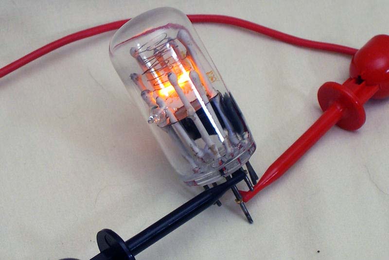
Illuminating a vertical Nixie tube.
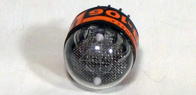
The HB-106 high redability Nixie tube.
Supplying the filament of a vacuum tube.
Burroughs Corporation was an early computer company that introduced the Nixie Numerical Indicator tube during the 1950s, although the design is attributed to the Haydu Brothers, who were already in business making electronic components and production tools for working glass. It is rumored that the Burroughs prototype was called “Numerical Indicator eXperiment 1” and the name ‘Nixie’ stuck. These devices were eventually displaced by lower voltage types (LCDs, LEDs, VFDs) that we know today, and US manufacture of Nixies ceased in the 1970s. There has been a hobby revival in using the original Nixie tubes and copies made by the Soviets (produced up until the late 1980s).
Most, if not all, experiments with Nixie tubes require around 200V up to about 10 mA. The original connection scheme applies high voltage to a single anode through a resistor (to limit the maximum current) and any one of the 10 cathodes is grounded through a switch or transistor. Glow discharge around the selected cathode shaped like a digit or letter makes a pleasing neon orange display.
There are vintage bipolar ICs from the DTL and TTL logic families of the 1970s to drive a single Nixie, but many experimenters roll their own circuits or adapt high voltage CMOS ICs to the task. Nixie cathodes that are turned off have about 50V bias, requiring high voltage devices to drive the tubes. Some Nixie driving schemes require a second supply voltage around one third of the anode supply (i.e., 60V) to power the CMOS IC or aid in controlling the Nixie display when driven within a multiplex scheme. Multiplexed displays use fewer high voltage devices and save power, space, and cost for the project. Unlike radio tubes (used as amplifiers and oscillators, mixers, etc.), Nixie tubes are cold cathode devices and don’t have heaters or filaments.
As Nixie tubes are no longer being made, to save the ones that we do have it’s wise to turn off the high voltage when it’s not needed. In a Nixie clock, this can be done at night or during the workday when no one is around. Controlled by the time keeping circuit or a proximity detector, the display wakes up when people approach. This requires shutdown of the high voltage controlled by logic (5V) level, as featured in this project.
For most Nixie experimenters, it’s easy to enhance a project with modern digital logic or microcontroller circuitry, which is geared to a 5V DC supply and was also added to this project.
Nixies found as NOS (New Old Stock) may suffer from storage damage and not work correctly. Often these tubes can be revived with a steady current above the normal design rating, applied for many tens of hours until the digits “clean up.”
I built my first HVPSU to test unknown Nixies found at hamfests or pulled from dead equipment. The project described here is ideal for off-line Nixie testing, burn-in, and recovery.
Parts List
| ITEM |
VALUE |
MOUSER PART # |
DESCRIPTION |
| C1 |
47u/25V |
5985-AFK25V47-F |
CAP 47 mF 25V ELECT VS SMD |
| C2 |
10u/16V |
5985-AFK25V47-F |
CAP 10 mF 16V VS ELECT SMD |
| C3,C4 |
1n0/630V |
81-GRM31BR72J102KW01 |
CAP 1000 pF 630V CERAMIC X7R 1206 |
| C5 |
10n/630V |
810-C3216X7R2J103K |
CAP .01 mF 630V CERAMIC X7R 1206 |
| C7 |
4u7F/450V |
647-UVZ2W4R7MPD |
CAP 4.7 mF 450V ALUM LYTIC RADIAL |
| C8 |
1uF/450V |
647-UVZ2W010MPD |
CAP 1.0 mF 450V ALUM LYTIC RADIAL |
| CN1 |
DC-JACK |
806-KLDX-0202-A |
CONN JACK POWER 2.1 MM PCB |
| CN2 |
22-27-2081 |
538-22-27-2081 |
CONN HEADER 8POS .100 VERT TIN |
| (ALT) |
22-03-2081 |
538-22-03-2081 |
CONN HEADER 8POS .100 VERT TIN |
| D1 |
YELLOW LED |
859-LTST-C150KSKT |
LED YELLOW CLEAR 1206 SMD |
| D2,D3 |
MURS140T3G |
511-SMBYT01-400 |
DIODE ULTRA FAST 1A 400V SMB |
| D4,D5 |
MMBZ5256 |
621-MMBZ5256B |
DIODE ZENER 30V 350 mW SOT-23 |
| DS1 |
NE2MINI |
606-2ML |
Neon 65 VAC .3 mA NE-38S |
| IC1 |
L7805 |
511-L7805CV |
IC POSITIVE REG 5V TO-220FP |
| IC2 |
MC34063SO |
863-MC34063ADR2G |
IC REG SW DC-DC INV 1.5A 8SOIC |
| L1 |
CDRH127/LDNP-101MC |
851-CDRH127LDNP101MC |
INDUCTOR 100 mH 2.1A SHIELD SMD |
| L2 |
CDRH127/LDNP-221MC |
851-CDRH127LDNP221MC |
INDUCTOR 220 mH 1.45A SHIELD SMD |
| Q1 |
MMBT4401 |
512-MMBT4401 |
TRANSISTOR GP NPN AMP SOT-23 |
| Q2 |
MMBT4403 |
512-MMBT4403 |
TRANSISTOR GP PNP AMP SOT-23 |
| Q3 |
IRF830A |
844-IRF830APBF |
MOSFET N-CH 500V 5A TO-220AB |
| R1 |
10K |
660-RK73H2BTTD1002F |
RES 10.0K OHM 1/4W 1% 1206 SMD |
| R1,R2 |
1K0 |
71-CRCW1206-1.0K-E3 |
RES 1.0K OHM 1/4W 1% 1206 SMD |
| R3,R4 |
562K |
660-RK73H2BTTD5623F |
RES 562K OHM 1/4W 1% 1206 SMD |
| R5 |
1K0 |
652-3306P-1-102 |
POT 1.0K OHM 6 MM CERMET TOP TRIM |
| R6 |
7K32 |
660-RK73H2BTTD7321F |
RES 7.32K OHM 1/4W 1% 1206 SMD |
| R7 |
100R |
71-CRCW1206-100-E3 |
RES 100 OHM 1/4W 1% 1206 SMD |
| R8,R9 |
475R |
660-RK73H2BTTD4750F |
RES 475 OHM 1/4W 1% 1206 SMD |
| R10-R13 |
1R0 |
660-RK73H2BTTD1R00F |
RES 1.0 OHM 1/4W 1% 1206 SMD |
| R14 |
100R |
71-CRCW1206-100-E3 |
RES 100 OHM 1/4W 1% 1206 SMD |
| R15-R18 |
10K |
660-RK73H2BTTD1002F |
RES 10.0K OHM 1/4W 1% 1206 SMD |
| TP1 |
+5V |
534-5001 |
TEST POINT PC MINI .040”D BLACK |
| TP2 |
TP_GND |
(Construct from 22 AWG tin copper wire) |
| TP3 |
HV1 |
534-5001 |
TEST POINT PC MINI .040”D BLACK |
| TP4 |
HV2 |
534-5001 |
TEST POINT PC MINI .040”D BLACK |
Downloads
High Voltage Power Supply (PCB Design Files)