“Ouch!” I exclaimed as I examined the almost perfect circle surrounding a stylized “M” (for Motorola) that was branded into the end of my index finger after touching the case of a power transistor to see if it was “warm.” This was my introduction to “heatsink selection for power semiconductors” I received as a young experimenter building a power supply — a lesson I have not forgotten several decades after the event. The purpose of this tutorial is to provide an introduction to basic concepts of heatsink selection and installation for power semiconductors, and possibly save you a few burned fingers and burned out devices, as well.
Power semiconductors (both transistors and integrated circuits) may potentially dissipate large amounts of electrical power in the form of thermal energy or heat when the devices handle large currents. In order to find the heat load in watts the device must dissipate, simply multiply the voltage dropped across the device by the current through it. For example, the device will dissipate 20W if the device current is 4A with a voltage drop of 5V. Internally, the heat is generated across the semiconductor junction (i.e., that location where the n-type and p-type semiconductor materials join inside the device). If the heat is not removed, the temperature across the semiconductor junction — referred to as the junction temperature (Tj) — will rise until it exceeds the maximum junction temperature (Tjmax) which usually leads to destruction of the device.
Just as important, it is necessary to keep Tj as low as possible to ensure the reliability, service life, and performance of the semiconductor device. Typical values for the maximum junction temperature specified by semiconductor manufacturers range between 125°C to 150°C, although some devices — the 2N3035 NPN transistor for example — are rated for operation up to 200°C. A rough rule of thumb is that the operating life of semiconductor devices decreases by half for every 10°C rise in temperature above 100°C — equivalent to an exponential decrease in operating life with increasing temperature. 1

FIGURE 1. Heatsinks for TO-39 and TO-220 case styles.
A heatsink is a mass of metal that conducts heat generated by power semiconductor devices to a location with a cooler temperature — usually the ambient air — where it is removed by natural convection. A properly designed heatsink will maintain the junction temperature of the semiconductor devices well below the maximum operating temperature while minimizing the impact on the budget of the project. Figure 1 shows several small heatsinks designed for TO-39 and TO-220 case styles which are suitable for dissipating a few watts of power and are compact enough that they could be mounted on the circuit board itself. Higher power dissipations in the tens of watts are achieved by mounting a large heatsink on the back of the chassis which maximizes heat dissipation due to natural convection (see Figure 2).

FIGURE 2. A power semiconductor with a TO-3 case style mounted to a heatsink attached to the back of a chassis.
Increased heat dissipation beyond that given by natural convection — available, of course, at increased cost — may be obtained by either forced convection provided by a mechanical fan or by circulating some type of liquid coolant through the heatsink to remove excess heat. The sidebar discusses the concept of a thermal circuit in order to define some common terms and introduces the mathematical description of the problem of transferring heat from the semiconductor junction to the environment.
To provide an example, we’ll apply this information to the problem of selecting a heatsink appropriate to provide adequate heat dissipation for a LM309 five-volt regulator used in a typical power supply application.
Heatsink Design Theory (Sidebar)
| Electrical Systems |
Thermal Systems |
| Quantity |
Unit |
Quantity |
Unit |
| Charge: Qc |
Coulombs |
Heat: QD |
Joules |
| Current: I |
Amperes |
Power Dissipation: PD |
Watts |
| Potential: V |
Volts |
Temperature: T |
°C |
| Resistance: R |
Ohms |
Resistance: θ |
°C/W |
TABLE 1. Analogy between electrical quantities and thermal quantities.
It is common to apply an electric circuit analogy in order to introduce the basic steady-state thermal resistance model that relates the quantities of heat dissipation, temperature rise, and thermal resistance. Table 1 shows that the electrical quantities of charge, current, potential, and ohmic resistance are analogous with the thermal quantities of heat, power, temperature, and thermal resistance, respectively. Because of this analogy, Ohm’s Law — which describes the relationship between voltage, current and resistance in an electric circuit — also describes the corresponding relationship between power dissipation, temperature, and thermal resistance in a thermal system or “circuit.”
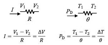
FIGURE 3. The application of Ohm's Law to electrical (left side) and thermal (right side) systems.
Figure 3 illustrates this idea and shows that just as the electric current I in a resistor results from the potential difference ΔV across a resistance R in an electrical circuit, thermal power flow PD produces a temperature difference ΔT across the thermal resistance in a thermal circuit. Solving the thermal equation given in the figure gives T1 = PD • θ + T2. For the problem of heatsink design, T1 is the desired operating junction temperature Tj; T2 is the temperature of the ambient air TA; PD is the power dissipated by the semiconductor device, and θ is the total thermal resistance between the semiconductor junction and the environment; by substitution this results in the thermal equation Tj = PD • θ + TA.
The thermal equation shows that two terms contribute to the junction temperature Tj. The first contribution is due to the power dissipation of the semiconductor device multiplied by the thermal resistance between the semiconductor junction and the ambient air. The second contribution is due to the temperature of the ambient air. In order to maintain the junction temperature Tj at a constant value, as the power dissipation PD increases, the heatsink designer must either apply air conditioning to lower the environmental temperature TA, or reduce the thermal resistance between the semiconductor junction and the ambient air. Normally, the most cost-effective approach is to install a heatsink with a small enough thermal resistance in order to maintain the junction temperature below some desired value, such as 100°C.
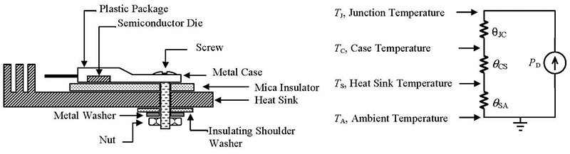
FIGURE 4. TO-220 case attached to a heatsink (left side) and equivalent thermal circuit (right side).1
Is it possible to verify that the heatsink installation is working? The right side of Figure 4 suggests a method for applying the thermal equation in order to verify that the heatsink is adequately sized. If the power dissipation PD and case temperature TC are known (perhaps by clamping a temperature probe to the case after applying a bit of thermal grease), the thermal equation becomes TJ = PD • θJC + TC. This relationship shows that the temperature at the semiconductor junction may be found by adding the case temperature TC to the product of the power dissipation PD and the junction-to-case thermal resistance θJC.
Heatsink Installation
A typical heatsink installation is shown on the left side of Figure 4 which shows the cross-section of a power semiconductor; in this case, one with a TO-220 package. When the device is in operation, the temperature of the semiconductor junction rises causing heat to flow from the semiconductor die through the metal case and mica insulator out to the metal heatsink where it is dissipated into the atmosphere. The metal heatsink is usually bolted onto the metal chassis so it is necessary to electrically — but not thermally — insulate the power semiconductor from the heatsink by separating the two with an electrical insulator such as a mica washer or silicon pad.
Typically, both sides of the insulator are covered with silicon thermal grease. The purpose of the grease is to fill any microscopic air pockets that would otherwise exist between the materials because air is a very good insulator. This produces air-free joints which minimize the thermal resistance through which heat must flow and reduces the temperature rise where different materials are joined. It is important to use just enough grease to fill the voids, but no more than that or the additional grease itself will serve as a thermal insulator, increasing the thermal resistance.
The right side of Figure 4 shows the equivalent thermal circuit. In this circuit, the total thermal resistance θ between the temperature of the semiconductor die and the ambient air temperature — given as °C/W — is the sum of the thermal resistance between the junction and the package case, θJC, the thermal resistance between the package case and the heatsink, θCS, and the thermal resistance between the heatsink and the surrounding air θSA or θ = θJC + θCS + θSA. Values for each of these thermal resistances are usually found in the manufacturer’s datasheet for the semiconductor device and listed in the manufacturer’s information for each heatsink. Approximate values for the junction-to-case resistance, θJC, are 0.5–2.5°C/W, for the package-to-case resistance, θCS, 0.5–1.5°C/W, and approximately 4°C/W and up for heatsink to ambient air, θSA, depending upon the heatsink’s shape, material, mass, and construction.
Heatsink Design Example
Let’s illustrate these concepts by designing a heatsink that will allow us to extract the maximum performance from a LM309 five-volt voltage regulator IC which has a maximum power dissipation of 20W 2. The LM309 was chosen because the manufacturer conveniently provides data that relates the device’s power dissipation, required heatsink thermal resistance, and ambient operating temperature which will allow us to verify our calculations.
First, it is interesting to note that the test conditions for the electrical characteristics specified for the device were taken at a junction temperature, Tj, of 25°C, which implies the device is either mounted on an infinite heatsink or the environmental temperature during the test was reduced by air conditioning. The datasheet also states that the maximum operating junction temperature for this device is only 125°C, so we will design the heatsink so that the device temperature does not exceed this value, although a more conservative design would use a lower value such as 100°C.
Substituting these values into the rearranged thermal equation in Figure 3 gives
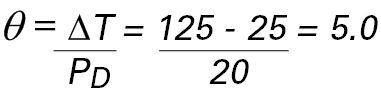
the maximum value of thermal resistance between the semiconductor junction and the ambient air that our design can tolerate without overheating. According to Note 3 in the datasheet, the thermal resistance between the junction and the package case, θJC, is 2.5°C/W. Additionally, typical values for the thermal resistance between the package case and the heatsink, θCS, are around 0.4-0.6°C/W when using a mica washer coated with silicon grease, so we’ll use a mid-range value of 0.5°C/W. Thus, the thermal resistance between the heatsink and the surrounding air, θSA, must be less than 5.0 – 2.5 – 0.5 = 2.0°C/W. This result agrees exactly with the manufacturer’s figure for maximum average power dissipation for the LM309K reproduced in Figure 5, which shows that a 2.0°C/W resistance heatsink is able to dissipate 20W of power at an ambient temperature of 25oC.
A review of heatsinks produced by one manufacturer (Wakefield Engineering) indicates that a heatsink thermal resistance of 2.0°C/W is just outside of what is possible without forced cooling. For example, the Wakefield 641A heavy-duty heatsink has a thermal resistance with natural cooling of 2.4°C/W, versus a thermal resistance with forced cooling of 0.9°C/W @ 250 LFM air flow. Thus, the designer must either limit the maximum power dissipation of the voltage regulator to 18.5W (100°C/5.4°C/W) or provide for forced cooling of the heatsink with mechanical ventilation in order to keep from exceeding the device ratings.
Finally — by way of comparison — Note 3 in the LM309K datasheet also states that the thermal resistance of the TO-3 case to ambient air, θCA, is approximately 35°C/W. Thus, without a heatsink, power dissipation is limited to less than 2.9W, also in good agreement with the result shown in Figure 5.
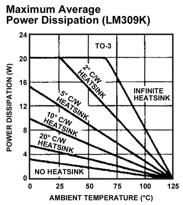
FIGURE 5. Maximum average power dissipation (LM309K)2. The arrow indicates the point on the figure that demonstrates that a 2.0°C/W resistance heatsink is able to dissipate 20W of power at an ambient temperature of 25°C which agrees with the sample calculation discussed here.
Conclusion
It is important to maintain the junction temperature of semiconductor devices below their operating limits in order to ensure the device’s reliability, service life, and performance. Usually, the most cost-effective approach to accomplish this is to physically connect the device to a heatsink by way of a conducting path with low thermal resistance.
This article demonstrated how to determine the minimum total thermal resistance by dividing the difference in temperature between the semiconductor junction and the ambient environment by the required power dissipation. Then, it is possible — after subtracting off the junction-to-case and case-to-heatsink thermal resistances from the total thermal resistance to select a heatsink with small enough thermal resistance to provide power dissipation that is adequate for the proposed application. NV
References
www.aavidthermalloy.com/technical/papers/pdfs/select.pdf
www.newark.com/pdfs/techarticles/mro/howToVerifyTheProperHeatSink.pdf
www.irf.com/technical-info/appnotes/an-1057.pdf
www.smoke.com.au/~ic/ham/heatsink.html
www.onsemi.com/pub_link/Collateral/AN1083-D.PDF
www.wakefield.com/PDF/thermal_tutorial.pdf
Footnotes
- Motorola Semiconductor Technical Data Sheet AN1083, Basic Thermal Management of Power Semiconductors, 1990.
- National Semiconductor LM109/LM309 5-Volt Regulator Data Sheet.