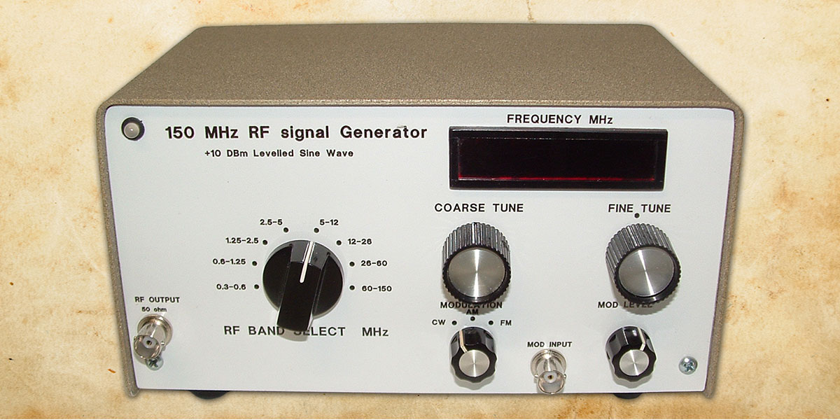
Once our interest in electronics is piqued, our inventory starts to grow — first in knowledge gained by books and select articles, followed by a small inventory of parts, and a few pieces of basic test equipment. We usually start with a simple DMM and some sort of power source. As time goes by, we accumulate a fair amount of basic equipment. However, no test bench is complete until it has an RF signal source of some type. What I will present here is a sweet little general-purpose RF signal generator that won't take up much bench space, will fill that missing gap, and can be built fairly cheaply.
Let me start with a brief overview of what’s out there. Signal generators come in a wide variety of flavors. Starting at the very top end would be a generator that oscillates at only one frequency that is extremely accurate, such as might be used by NIST (National Institute of Standards). These are primary frequency standards and time bases by which all other frequencies are referenced to. They have incredible accuracy and can cost upwards of $100,000.
Next in line would be very high-end generators with super specs of accuracy and stability, along with any type of modulation that’s available. Today, these mods can be quite complex. Then, we drop down to mid-range generators that — although they still have excellent specifications — will be more application-specific (limited frequency bands, etc.) rather than “all purpose.” Many of these are slow in use due to programming and a myriad of pushbuttons. Once you pick your chosen frequency, they perform excellently, but they can cost anywhere from $1000s to $10,000s.
One corporation I worked for involved using a very complex microwave generator which had excellent specs in a myriad of features and — although you could perform just about any frequency related test with it — it was also slow to get to each specific point of interest. The user manual was a full 3” thick and it would probably take a year to become totally proficient at using this generator. One other thing was that it reportedly came with a $38,000 price tag.
At the very bottom of the heap is the general-purpose generator which may run from $200 upward. These are basically intended for consumer product service and non-critical design work. Although they lack the features and quality of higher-end generators, they have several glaring advantages: ease of use, the speed to run the gamut of their entire output range, plus (the biggest merit) very low cost. No array of pushbuttons or programming here. Just flip a switch, turn a knob, and rapidly get to where you want to go. Their intended market is directed at ham operators, hobbyists, or people that like to tinker with electronics which would be people just like us. Having tried several commercial general-purpose generators over the years, I felt that better performance could be achieved which set the stage for designing one from scratch. These generators were priced in the $180 to $250 range.
The one I am presenting in this article will have superior performance in all specs and (assuming the builder has a moderate junk box of components) can be built for about $50. This does not include a commercial housing, which at a minimum would cost $75 and up. As I will explain later in this article, there is a procedure for forming your own.
Theory of Operation
The heart of this unit is the RF deck. If you read my article 180 MHz Sweep Generator, you'll see a very similar design here. I covered the theory of this section quite thoroughly in that article, so I won’t dwell on it too much now. I have used this style in seven or eight different designs over the years, which ran the gamut of simple one frequency oscillators to complex phase lock loop synthesizers, and it has always been a solid performer.
To begin with and referring to Figure 1, the RF deck is based on a marvelous chip developed by Motorola in the early ‘70s. (So popular, in fact, that it is still being produced today — almost 40 years later!) The IC is a MC1648 DIP. However, current versions are in SMD form and go by the name of MC100EL 1648, but are still available in the DIP version. This chip is a member of the ECL (emitter coupled logic) family and is basically a high speed LC oscillator circuit. It can cover a large range of frequencies from MF, HF, and well into VHF portions of the RF spectrum. It is easy to use and has built-in AGC (automatic gain control) that can be tailored to your particular needs.
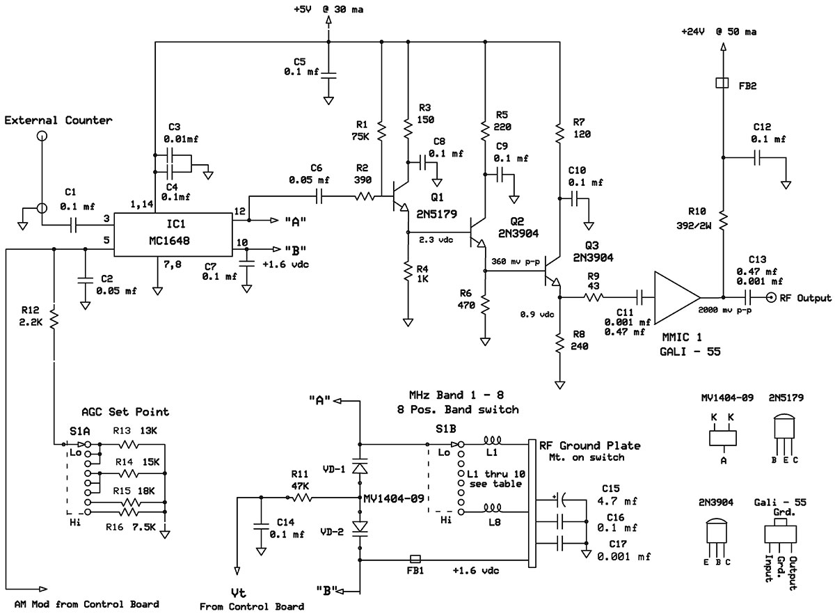
FIGURE 1.
In this design, various resistors (R13-R16) are switched in as the frequency bands are switched. The tank circuit impedance will vary over a tremendous range when a fixed capacitance tuning value is used for all bands, but by trimming the AGC bias for each range it will do an excellent job of maintaining a leveled amplitude output from the tank circuit. It also has an output buffer amplifier that I use in a non-traditional way for an external counter.
The LC tank circuit is comprised of switched inductors L1-L8 and the capacitance of varactor diode VD1 and VD2 (which is actually two diodes in one package). Varactor diodes exhibit a changing PN junction capacitance with a changing DC negative bias voltage across that junction. The SMV 1404 series are of the Hyper-Abrubt type, and have the highest Tr (tuning ratio) capacitance vs. bias voltage and linearity of all the various styles of varactors. They have a Tr of 16:1 or higher, and over a one octave range of tuning which gives excellent linearity.
In my opinion, the 1404 series of varactors is the greatest varactor ever produced for projects like this since they cover MF through VHF bands of frequency. As luck would have it, they are also the most difficult to obtain.
Rather than take the output from the normal amplifier port which can be somewhat distorted, I chose to take it right off of the attached LC tank circuit which has a very clean wave form, thus saving the amp port for external counting operation. By designing it in this fashion, it needs a lot of buffering from the high impedance tank circuit to the 50 ohm input of the final MMIC (monolithic microwave integrated circuit) amplifier. This is the job of Q1, Q2, and Q3. These are all cascaded emitter followers and start with Q1, which has a very low input capacitance.
Since high frequency followers with an inductive element in their base circuit can sometimes be unpredictable and break into oscillation, a “stopper resistor” R2 was added in series to the base input. This has the effect of dropping the “Q” of that area’s parasitic elements, and ensures that any parasitic oscillations will not occur. Q2 adds yet more buffering, and Q3 is configured to drive the final amplifier (MMIC 1). With the addition of R9, this gives a good 50 ohm impedance match which is required here.
The MMIC amplifier is of a family of ICs known as gain blocks. Their input and output impedance is always 50 ohms, and they have a fixed gain with no control over that function other than adding attenuators to adjust the input or output level. This particular one has a 20 dB gain (X10 voltage) and is very flat from DC to well into the GHz range. The drawback of having no internal gain control is completely overshadowed by their utter simplicity: Just solder it in and go!
FB1 and FB2 are ferrite beads that “gobble up” any high frequency components on those leads as we want to keep these wires very quiet. The GALI-55 amp wants to see a 50 mA constant current supplied to it rather than a constant voltage (approx. 4.5 VDC). You might be wondering why I designed its power source the way it is shown, which is quite inefficient to supply 50 mA to a low voltage device. It all has to do with bandwidth ratio and not just merely bandwidth.
If I were designing a generator for, say, an output of 1 GHz to 1.15 GHz, that would still require a bandwidth of 150 MHz. However, I could then use one RF choke for the load and it would remain relatively constant over that ratio of change. This would only require a five volt feed to power the MMIC at 50 mA due to the very low DC drop in that choke. Even though I am covering the same bandwidth with the presented signal generator, that method would not work. The reason: bandwidth ratio.
The higher speed generator has a ratio of 1.15:1, and one choke would present a constant load over that range. My generator has a ratio of 500:1 (0.3-150 MHz). No single choke could even come close to presenting a constant load over that kind of range. So, I am committed to a resistive load for consistency over the complete range.
Doing some math, I determined that the optimum value of approximately 392 ohms is as low as I would want to go. Carrying this further, 392 ohms/50 mA = 19.6V and adding another 4.4 volts across the MMIC results in the necessity for a 24 VDC supply. Wasteful, yes, but that is one of the prices you pay for a wide bandwith ratio amplifier. The manufacturer highly recommends that you do not use a constant current supply in this circuit.
Figure 2 is the control circuit and front panel controls which are pretty simple and straightforward. IC1a drives the MC1648 AGC pin 5 directly for AM modulation. Being a follower type of configuration, its amplitude will remain constant despite changing loads due to the AGC section of the band switch presenting different loads depending on its location. Diodes D1 and D2 clamp the input signal circuit for a maximum signal level of 1.4 volts P-P. This is for the protection of over-driving P5 of the MC1648.
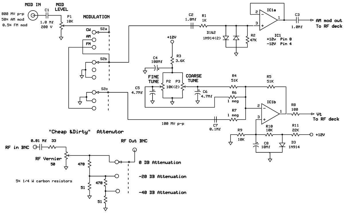
FIGURE 2.
R1 limits the current during periods of heavy clamping. The external AM signal is fed into the mod input jack to P1 level control and through modulation switch S2 when in the AM position. For FM modulation, the signal is brought in through the same path other than the S2 switch position. From there, it goes into IC1b’s summing point. When no modulation is desired, S2 is set at the CW position (Continuous Wave) and mod input capacitors C2 and C7 are grounded to keep these lines quiet.
IC1b has several functions: It sums all the voltage inputs of the coarse tune control, the fine-tune control, and the FM mod input (when used). Op-amp summers are nice for this type of adding as there is absolutely no interaction between the inputs feeding it. As can be seen, the tuning controls are well filtered to keep this line as quiet as possible. The output of IC1b requires a 100 ohm resistor R8 in series with it due to the necessity of driving a large filter capacitance when entering the Vt connection on the RF board. Op-amps can become unstable, driving large cap loads; R8 is the cure for this. Since the tuning span Vt has to cover a range of -6.1 volts to +0.6 volts, an offset in the op-amp output of +0.6V is needed for its starting point. This is accomplished with R9, R10, R11, and D3 at its positive input.
D3 provides a convenient source of 0.6V, but also performs one other function. It has a PN junction drop of 2 mV/degree C which is the exact opposite to the tank circuit varactor diode Vd1, Vd2. This helps to stabilize the oscillator frequency in that respect (ambient temperature) by putting a slight shift in Vt vs. temperature. It’s not perfect, but helps.
The power supply shown in Figure 3 is pretty straightforward and does not need much explanation. It might look like overkill, but was the best I could come up with considering the variety of voltage sources required. When it comes to op-amp design, I am a big fan of split supplies. The 5V supply has the capability of supplying much more current than what is needed for the RF deck, but I beefed it up to cover the counter and prescaler options. It could also be used to supply a rear panel jack for powering add-on outboard circuits. Also, I split up the 5V through two different regulators to minimize interference on the supply lines feeding the analog portion (RF deck) and the digital portion (counter, etc.).
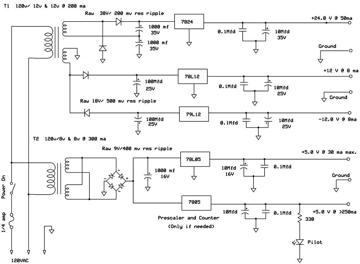
FIGURE 3.
Construction
Before I get too far into this section, I will not go into a lot of details in all aspects of construction as it would take too much magazine space to discuss everything involved. Fear not, though, for those that desire to build this generator, I have a huge packet of info that I can email to you. This will include full screen pictures, actual size drilling templates, detailed layouts, construction tips, some artwork, and lots of technical data. Most of it is included in the downloads at the end of this article.
There are just two basic subassemblies that will be installed in this chassis: the RF deck and the power supply deck. The control circuitry is so minimal, I built it up on a small printed circuit board (PCB) and screwed it down to the power supply board. This simplifies assembly and testing before each unit is permanently installed.
The RF deck shown in Figure 4 was built on a 2” x 2-1/2” single-sided PCB using typical RF prototype construction. The MC1648 and R1, Q1, Q2, and Q3 are the only components mounted on the laminate side of the board. Be sure to use a socket for the IC. Since only eight pins are used in this 14-pin chip, seven pins can be removed before installing it.

FIGURE 4.
These are conveniently located as every other pin and makes soldering underside components a lot easier. After drilling all the lead through holes, all but the ground lead holes are reamed out with a larger drill of about 5/32” to give clearance from the lead to copper foil. The GALI-55 will require two small islands for input and output connections. The SMV1404 varactor is quite small and despite SMD soldering, I found an easy way to install them.
I first cut a piece of plastic laminate (formica, etc.) to 3/8” x 1/4” and then tack the varactor to the laminate with a spot of super glue. Make sure the varactor is positioned laying on its back with its “feet” pointing up as this makes final soldering easier. This assembly is one of the last components I install, and again a dab of glue helps to adhere it to the PCB. When all leads that go to this device are soldered to their proper nodes, cut the free end to the exact length; then, a quick tack solder to the chip pins completes installation. I use #24 or #26 wire here.
The rest of the active components are inserted and their leads are used as solder tie points. All other circuit nodes above ground get soldered to insulated standoffs. The two standoffs (A and B) near the MC1648 pins 10 and 12 will be used for primary testing and final S1 band switch connection. When doing RF circuit construction, always keep two things in mind: an RF ground plane is essential and lead lengths must be short. How short? Well, RF design engineers have an old saying, “if you can see the leads, they are too long.” Impossible in the real world, but you get the idea. The PCB is mounted to a subchassis with three 1/2” metal standoffs. This chassis will include a 3/8” hole in its vertical section to mount the band switch. Set this sub-assembly aside for now; further testing will be done later.
The RF band switch (S1) shown in Figure 5 is a two-pole eight-position wafer switch. I used an old ceramic Centra-Lab 4 deck wafer switch that I had on hand. All decks are held in place with long #4-40 screws and spacers. These switches are easy to disassemble and rework. All wafers have a full 12 positions on them, and one metal bracket with bending tabs is used to lock the stop for the actual number of positions desired.
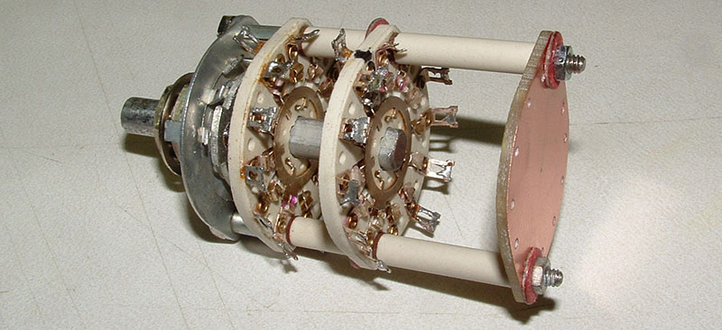
FIGURE 5.
The number of decks on the switch does not matter, but you need at least two decks. Unnecessary decks are discarded, and the wafer shaft gets cut back so it only drives two wafers. Since the tank circuit coils on the RF deck have +1.6 VDC of bias voltage on them, we need an RF ground on their low side which has to be isolated from DC. This is accomplished by cutting a piece of single-sided circuit board to the approximate shape of the switch wafer. This is then aligned with the wafer, and the position tabs and mounting bolt locations are then transferred to the ground plate.
Since there are no moving parts involved here, the plate requires no drive shaft connection. The mounting holes will be drilled for #4-40 clearance and the coil lead holes will be about 0.050”. The ground plate will be mounted with the foil side to the rear. When ready to install the coils, one end is slid through the switch’s position tab as far as it will go, then the other end trimmed to allow it to pass through the ground plate. Center the coil and solder, and trim the overhanging ends.
When purchasing your switch, there are several things to keep an eye on. Look for mounting bolt construction and a full 12 position tabs on each deck. Also look for the least amount of metal brackets that seem unnecessary. The number of decks is unimportant just as long as it has at least two as mentioned, because the switch will ultimately be reworked to have two switched wafers (S1A and S1B) and one ground plate. The switch then needs to end up with two wafers set for eight positions by adjusting its position tab plate; the shaft cut back to a length long enough to operate these wafers if necessary; and two #4-40 bolt and spacers to hold the whole thing together.
Since #4-40 bolts are hard to find in longer than 2” lengths, you can use threaded rod if necessary. I needed two 1/8” lengths on my switch, and a trip to the local hardware store found the threaded rod. Again, set the completed switch aside for now.
The power supply/control board construction is quite straightforward and — with Figure 3 and Figure 7 — does not need much further explanation. I used a piece of thick laminate (formica) drilled for component lead holes after I patterned the layout. The major components were placed in the board with a dot of super glue and then point-to-point hard wiring. Ugly, yes, but it will never be seen and I have rarely had any problems with my power supplies. It would have been nice if I could have located one transformer with both high and low voltage secondaries to make it simpler, but nothing showed up when I searched.
However, I have been using Tamura transformers in quite a few of my designs lately. They come in just about any voltage/power level that one would want and are very reasonably priced. The frequency/mod control board contains almost all the components shown in Figure 2. Only the pots and switches are on the front panel, plus a few components that directly interconnect these parts. The mod level control (P1) shown in the Parts List is a slightly smaller version of P2 and P3, and was chosen only because its size fit better into the panel space available there.
The enclosure was formed with four pieces of aluminum sheet stock and a foot or so of aluminum 1/2” angle. The dimensions are approximately 9” wide x 4” high x 6” deep. The first piece formed was the cover. Then, all other pieces were cut to fit which are: the front panel, rear panel, and bottom. I usually make the bottom and back out of one piece cut to size, and then have my local sheet metal shop put the required 90 degree bend in it, but I was in the middle of a snow storm and really wanted to finish this up. So, I cut two pieces and joined them with 1/2” angle using pop rivets and #6-32 screws as can be seen in Figure 7.
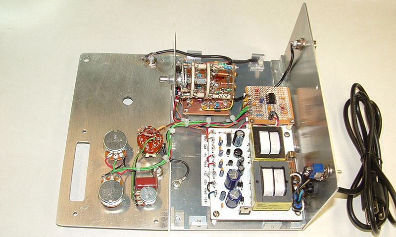
FIGURE 7.
The cover, front, and rear panel are 1/16” aluminum and the bottom is 1/8” aluminum; all #5052 grade material. This grade is easy to bend and still has good machining ability. It can be cut by a table saw with a carbide blade very easily and, in fact, most woodworking tools with carbide cutters can machine this grade. I bend the pieces in a vise with wooden blocks supporting the bend line area, but I can only bend up to 1/16” thick stock. Beyond that, I go to my sheet metal guy. The cover and front panel are attached to the bottom plate with six 3/4” long angle brackets (as shown in Figure 7) in much the same way as the rear panel was. Next, do the front panel machining and art work, spray paint the cover the color of your choice, and attach the feet. You are now done.
I did drill a 3/8” hole in the rear panel to install a BNC connector for external frequency counting. As you can see from Figure 7, the 120 VAC power-on switch is mounted right above the incoming power cord. I have grown fond of this method the last several years as it saves front panel space, and keeps 120 VAC and its fields concentrated in one spot so I don’t have to snake it all over the place to put it on the front panel. (As mentioned earlier, I have more info on this subject available.)
Final Checkout and Operation
At this point, we are ready to do some final testing on the subassemblies and check them out before installing them permanently in the chassis. Starting with the power supply deck, wire up 120 VAC to it and check the outputs for correct polarity and voltage. If all is well here, you can use this to power the RF deck for testing. With the RF deck mounted in its subchassis as shown in Figure 6, temporarily tack a 15K resistor from the AGC input (low end of R12) to ground just for these tests.
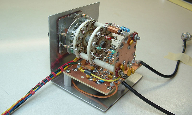
FIGURE 6.
For a tuning control, you can temporarily wire a pot and resistor to the Vt input on this deck. Do not install the band switch at this time. Do not connect the 24 VDC supply at this time, either. Do connect the +5 VDC to the deck. You will need all of your coils at this time, plus a 100 µH,10 µH, and 1 µH for these tests. For each of these, tack one coil at a time onto standoff posts A and B. With a scope and frequency meter attached to the emitter of Q3, you should see approximately 360 mV of clean sine wave with each coil used. Don’t worry about the exact amplitude as this will be adjusted at a later point in testing.
With any coil installed, vary the tuning range and you should see a bit more than one octave of frequency span for each coil. The exact frequency is not important here, but each coil should give about a 3:1 frequency shift as you increase the coil inductance. Shut off power to the deck and temporarily connect a 51 ohm 1/4W resistor from the RF output jack to ground. Power up and scope this point. There should be about 2,000 mV P-P of clean sine wave here. If all is well, power down and remove the coil.
Prep the switch by soldering a 1” piece of wire to the S2B wiper contact. Also, one item worth adding is a thin 1” square shim of pre-tinned copper with a 3/8” hole in its center, shoved onto the switch mount bolt. This makes it so much easier to install the AGC resistors by giving a convenient ground point. Now, install the switch so that the wiper contact of S2B is positioned right over insulated standoff A. This should be about 1/2” above the post.
Tighten the switch mounting nut. Solder the wiper lead and install the wiring from the RF ground plate on the switch to post B. Add a wire with FB1 from S1a wiper contact to the low end of R12. Now, the individual band coils will be installed.
Starting with the lowest band and as each coil is installed, a frequency check will be made for span and correctness of its labeled bandwidth. The band 8 inductor (see Parts List) is just a 1-1/2” piece of bare #22 wire. Start here with a piece a little longer than 2”, then trim back as needed while doing the band tests. After you cut it to the length you need, just wind up one or two loose loops if necessary to fit in the space allowed. This will make virtually no change in inductance as opposed to the straight wire.
The coils that you use may not be the same value as mine due to parts tolerances, and there are a lot of tolerances to consider here. The SMV-1404 is a very repeatable component, while the coils can vary by 5% or more. Resistors, pots, and the list goes on. The laws of probability state that half the tolerances will be positive, the other half negative, and they will cancel each other out. Murphy’s Law says all tolerances will add in the same direction and render the design useless. In the real world, it’s never this bad, but still something to be aware of.
When you purchase coils, it would be a good idea to get a variety close to the Parts List values and some at about 5% of the listed values. I actually ordered 50 for this project since it was a new design. The parts are dirt cheap, and it would be a shame to come up short and have to order 80 cents worth of coils for $6 postage. Besides, you can always use the extra in other projects.
Let’s get back to installing the tank coils and what you want to achieve here. Strive to get the span needed for the panel labeling (shown with some overshoot) on each end of that band. I ended up with an average of 5% on the ends, but some were as close as 1%. The AGC resistor installation and warmup will shift that span by a very small amount. The actual total span of frequencies should be 0.3 MHz to 150 MHz with no gaps between bands. Mine runs 0.295 MHz to 162 MHz. Having plenty of overshoot is okay, but the most important aspect is that the band switch labels guarantee their stated bandwidth. Can’t quite fit everything into my labeling? You can always tweak the Vt voltages to make it fit. Maximum voltages should be no more than +0.7V on the low end by virtue of R9 and R10 on the control board, and -7.0 volts on the high end of the tuning pots by changing R3. Still can’t get everything to fit? Then do what I did: change the artwork on the front panel labels.
When all is set and done with this part of the testing and you have a minimum warm-up period (10 min), you can now adjust the AGC voltage for each band. Start with the lowest band first. Hopefully, you own a resistor substitution box to connect to the S1A wiper and ground. Load the output with a 51 ohm resistor and connect a scope at that point. As you run through each band, adjust the resistance for +10 dBm (2,000 mV P-P) output and make sure you tune through the band to select for the best overall flatness. Make note of the R value for each band as you proceed.
You will probably find the same value of resistance will work for several bands, minimizing the resistors ultimately needed. One word of caution here: I use a Tektronix scope with a 350 MHz -3 dB bandwidth, but it is only perfectly flat out to 100 MHz. Beyond that, it rolls off in typical Gaussian fashion. However, I have had it calibrated for sine waves all the way to 500 MHz in a 50 ohm environment. Now, I have a look-up table so that regardless of what the scope displays, the table tells me what the correction factor needs to be. Most scopes will do a fair job up to 40 MHz or 50 MHz, but if you do not trust your scope beyond that point, then use the AGC values shown in the print for band 8. At this point, you can complete the unit and close it up.
Closing Notes
The output of this generator has an exceptional amplitude response of ± 0.1 dB on bands 1 through 7, and ± 0.5 dB on band 8. This is due to the built-in AGC circuits of the MC1648. I did not do an FFT on the output, but after looking at scope sine wave presentations for over 40 years I have developed a pretty good eye for distortion, and would judge spurious and harmonics to be a good 30 dB below the output level. That is a clean sine wave and very respectable for this type of generator. LC oscillators do not have the long term stability as their crystal referenced “big brothers” do, and usually will drift 500 ppm or more over a given time. Although this one is no exception to that rule, it out-performs those figures by quite a bit.
After a one hour warmup, I performed many tests for short-term stability of 15 minute periods. I did this for each band at the low, mid, and high ends of their ranges — 24 tests in all. The best case was 2 ppm drift in that time and the worst case was 98 ppm. The rest varied from 20 to 80 ppm, with 50 ppm being a good overall average. So, I could conservatively spec the overall short-term stability at 100 ppm which is quite good for an LC oscillator. I was also pleasantly surprised that I could easily inject a signal into the input of a narrow band land mobile receiver at 155 MHz and hold that input for quite a while — although it did show a sensitivity to load changes in those frequencies.
The external modulation input was set arbitrarily at 800 mV P-P for all inputs. In the AM mode, 50% modulation can be obtained before soft clipping and then hard clamping occur. This function has a good linearity figure of 3% and about 15 mV P-P for each percent of modulation sensitivity. The clamp circuit prevents the MC1648 from damage due to accidental over-voltage of input here. Without the clamp, it has the same linearity up to 90% mod. Unless you are feeling lucky, do not bypass this feature. The standard test signal for AM is 30%, so this is achieved and then some.
The FM mod input is attenuated quite a bit in the summing amplifier and is not so prone to over-voltage. At a full 800 mV P-P, it will produce a deviation of approximately 0.5% of the carrier frequency. A calibrated FM deviation is very difficult to achieve and would require twice the circuitry as the entire generator with specially machined switches, so it was not even considered for this design. However, if you have a few “pet” frequencies that you would like a known deviation for, there is one method of achieving this. Set the generator to the carrier frequency desired and carefully inject a DC voltage of zero at the junction of C7 and R7 on the control board, with the mod control set for FM operation. Note the frequency and slowly increase the DC voltage until the carrier frequency increases by the amount of deviation desired. An AC P-P voltage that is the same as that DC voltage will now give the exact amount of deviation you want. If you do this often, a rear panel jack connected to that point would make things easier. Just keep in mind that the DC eventually winds up on the Vt line to the varactor because there is no blocking capacitor in that path.
There are a couple of changes that I made that are not shown in the images. On the RF board, I extended the leads of R10 to 1/2” on both ends so as to mount it higher off the board, and bent it slightly away from the board. This resistor dissipates one watt, and was dissipating a lot of that heat into the copper foil. This is the one exception to the “short leads” rule. The added inductance of the leads will only affect band 8 by increasing the MMIC’s load impedance. The effect is so minimal that it can be ignored. It still couples some heating to the board and — along with the upside down mounting of the MC1648 adding yet more board heating — they will raise the board temperature about 13 degrees F above the work area’s ambient.
Of course, some of that heat is generated by transformers, regulators, and such. This is why it takes about a full hour warm-up to stabilize. However, after a couple of minutes, the generator is ready for use. Just let it warm up for an hour before doing critical work such as IF alignment, etc. The other change was adding a 1” square of thin aluminum to the 7824 regulator tab in the power supply as it tended to run too hot without this.
I did not design an RF attenuator in this unit to keep its footprint as small as possible. Years ago, I bought a really low priced HP attenuator on eBay. It will attenuate 0-130 dB in 1 dB steps, and with HP quality. I find that I use this attenuator even with equipment that has one built in due to its wide bandwidth and precision.
In my sweep generator article mentioned previously, I show construction of an attenuator that won’t bust your wallet. It has decent performance to upwards of 200 MHz and about 5% accuracy. This is a four step 0-40 dB in 3 dB steps. This could be expanded to 0-100 dB in 1 dB steps by using 27 5% 1/4W resistors and nine DPDT mini switches, plus some double-sided circuit board for a housing at a cost of maybe $30. The switches could be mounted vertically in a single column on the left side of the panel.
Either way, you would have to add another 1-1/2” to the panel width to accommodate these. (I could include this in the email packet.) If you are desperate for an attenuator, the “cheap and dirty” version shown in Figure 2 will suffice as far as more power/less power goes. Also, there will be an insertion loss of 3 dB (for the MMIC protection) and it will not be calibrated. For five dollars in parts, it will get you by.
As to what I might change in the future: replacing the fine-tune pot R2 with a three-turn pot for even finer adjustment; and adding an internal tone oscillator with 800 mV P-P output. Then, I’d connect this to the front panel jack via a miniature SPDT toggle switch.
I am always changing designs for the better as new ideas and components become available. I do have an outboard clock generator design for this generator included in the email packet. It runs at exactly half the frequency of the RF output feeding it, and has a perfect square wave with rise and fall times in the low nanoseconds. When doing this project, take your time and double-check connections as you proceed. Most of all, have fun! NV
PARTS LIST
| ITEM |
DESCRIPTION/PART # |
SOURCE |
| All resistors are 1/4W carbon film 5%. All capacitors are in microfarads. Special parts are listed below. |
| RF DECK: |
| IC1 |
MC1648 DIP |
MC100EL1648 SMD |
| VD1, VD2 |
SMV1404-09 |
|
| S1 |
Two-pole, eight-position wafer switch |
|
| Q1 |
2N5179 |
|
| Q2, Q3 |
2N3904 |
|
| MMIC |
GALI-55 |
|
| FB-1 |
FB43-226-RC |
JW Miller |
| FB-2 |
FB43-287-RC |
JW Miller |
| R11 |
47K, 1/8 watt optional |
|
| R2 |
390 ohm, 1/8 watt optional |
|
| R10 |
392 ohm two watt CPF2392R00FKR36 |
Vishay/Dale |
COILS: BOURNS OR FASTRON CONFORMAL COATED
*See text |
| L1 |
2500 µH |
|
| L2 |
680 µH |
|
| L3 |
150 µH |
|
| L4 |
38 µH |
|
| L5 |
9 µH |
|
| L6 |
1.8 µH |
|
| L7 |
0.33 µH |
|
| L8* |
40 nH |
|
| CONTROL BOARD & FRONT PANEL: |
| IC1 |
TLO82 or TLO72 |
|
| D1, D2, D3 |
1N916 or equivalent |
|
| P1 |
10K ALPHA |
RV24AF-10-40R1-B10K |
| P2, P3 |
10K ALPHA |
RV16AF-10-20R1-B10K |
| S2 |
ALPHA four-pole three-position wafer |
SR2511F-0403-19ROB-E9-N-W |
| C1 |
1.0 MFD 200V |
(or as low voltage as you feel safe with) |
| Potentiometers and switch available at Mouser.com. |
| POWER SUPPLY: |
| T1 |
120V:24V ct @ 0.25A 3FS-424 |
TAMURA |
| T2 |
120V:8V/8V@ 0.3A 3FS-316 |
TAMURA |
| REGULATORS: |
| 7824 |
|
|
| 78L12 |
|
|
| 79L12 |
|
|
| 78L05 |
|
|
| 7805 |
|
|
| |
|
|
| MC1648 |
|
|
| MC100EL1648 |
|
Mouser, Digi-Key |
| VD1, VD2 |
|
Contact author ([email protected]) |
| GALI-55 |
|
MINI-CIRCUITS.COM |
| Coils |
|
Mouser (usually $0.2-0.4 each) |
| Resistors |
|
Mouser Electronics |
| S1 |
|
|
| FB-1, FB-2 |
|
Mouser Electronics |
| |
|
|
| Transformers — Mouser or Digi-Key (www.digikey.com) |
| Regulators — Just about anywhere |
| MC1648: Datasheets are easily obtained through Google. |
| GALI-55: Datasheets at MINI-CIRCUITS.COM. |
| SMV1404-09: I stock these. |
Downloads
What’s in the zip?
Extra images and Schematics