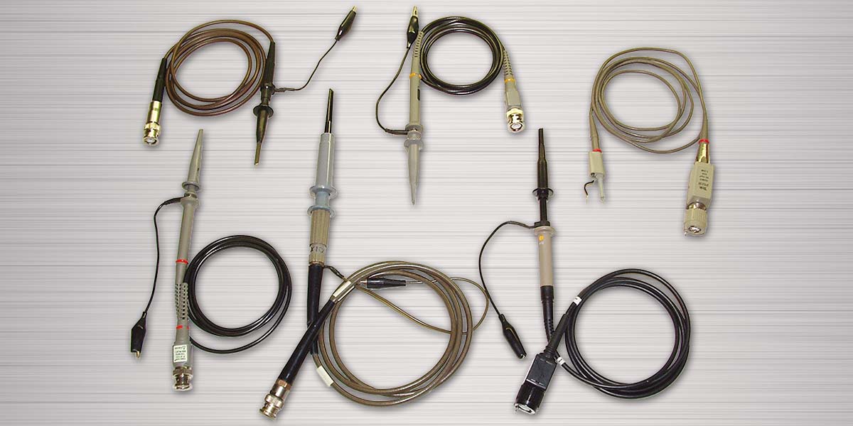
So, you made a great deal on eBay for a quality wideband oscilloscope along with some decent after-market probes, and UPS has just dropped it off at your doorstep. You anxiously tear open the package, power the scope up, and spend the next two hours at your test bench familiarizing and checking it out with your function generator. Everything works and appears to be correct — great! Now it’s time to examine the operation on a host of prototypes you have completed recently. Time to see the real deal on how these circuits are actually performing — things that your old worn-out Heathkit scope’s results could never have been trusted for.
Eeks : Problems!
The first circuit you look at with one of your 10X probes is a wide band amplifier. The results are disastrous. The frequency response is terrible; rising and falling in amplitude across the spectrum and with a much lower bandwidth than expected. In a cascaded section, one amp’s output is too high and the following amp’s output is actually lower than the one feeding it. Yikes! You switch to another probe and get the same results! You also notice that at the higher frequencies, moving the probe or cable changes the displayed amplitude. Next, you frantically look at another prototype containing an oscillator and a couple of buffers to an output jack. Connecting a probe from channel 1 to the output jack verifies that a signal is present there. You connect a probe to the scope’s channel 2 and probe a section in the oscillator and see no signal at all. How can that be as you previously saw an output at the output jack?
Looking back at channel 1, the former signal is also missing. Moving the channel 2 probe to a different section of the oscillator, you now see a signal on both channels and at this point are somewhat confused. One last prototype that is supposed to produce fast rise time pulses is probed and the rise time is much slower than expected with a lot of overshoot and ringing at its leading and trailing edges. Oh no, you are thinking. My prototype designs are terrible and the new scope is defective! Well, don’t throw your protos in the trash bin and send the scope back to the seller just yet. If your scope passed your initial tests, it’s probably working okay. If you have done similar protos in the past, then for the most part, they are probably doing at least a fair job. There is a very good chance that the problems lie in your probes and/or your probing!
Examining the Source of the Problems
You are probably thinking that since the scope has a 300 MHz bandwidth and the probes are rated at a 250 MHz bandwidth with a 1.4 Nsec rise time, they should give good performance up to 200 MHz and beyond — which they will under the right conditions. The key word here is right. Let’s cover a few things before we dive into probes. An oscilloscope’s rated bandwidth is the point where the displayed signal amplitude vs. frequency drops to -3 db (70%) of its DC or very low frequency value when a leveled sine wave source is feeding the vertical pre-amp(s). In scopes that follow a Gaussian response curve (and almost all do), this will follow a very flat frequency response to 1/3 of its rated bandwidth and then drop at an increasing rate to its -3 db point (i.e., 300 MHz bandwidth; DC to 100 MHz flat response).
However, this doesn’t mean that there won’t be peaks and dips along the way. In quality scopes, these are minimized. A probe with the same bandwidth spec as the scope may degrade this performance by virtue of its -3 db BW adding to the scope’s -3 db bandwidth, therefore intensifying the loss at the limits of their individual stated bandwidths. Some manufacturers design probes to match their line of scopes to preserve their rated bandwidth or even extend it slightly. Now let’s look at how a probe gets its rated bandwidth specs.
This is done in a lab environment using sine wave generators with a 50 ohm source impedance immediately terminated with a 50 ohm load that has a BNC jack built into it. The ground lead and clip tip (witch’s hat) are not used in this setup, but rather the tip has a special tip-to-BNC adapter that matches up to the termination jack. This effectively removes most problems associated with ground leads (as will be discussed later). Also, the probe tip is looking into an equivalent 25 ohm impedance by virtue of the generator source impedance (50) in parallel with the termination impedance (50). This constitutes an almost ideal condition for measurement, but rarely is the normal setup for probing in the real world.
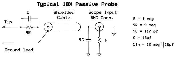
FIGURE 1A
Figure 1A shows a typical 10x passive probe connected to the scope’s vertical input and the standard 10 megohm input resistance that it presents to all circuits probed. It also presents a capacitive load on those circuits. This is the series combination of C and 9C. The typical capacitance the circuits under test will see at the tip will range from 10 to 14 pF, so I will use 12 pF as a middle of the road spec. Scopes have a certain amount of inerrant input capacitance, along with the probe’s cable, etc., connected to it. To obtain a flat frequency response in a resistive divider network, the time constant of the probe’s attenuator network (9R in parallel with C) must exactly equal the time constant of the probe cable and scope input values (R paralleled by 9C).
Since the probe’s tips are constructed with a fixed value of resistance and tightly controlled parasitic capacitance C, the RC values on the scope end must be adjusted to exactly match this. This is done with a capacitive trimmer mounted in a termination box which is attached to the cable’s BNC connector for the scope.
As mentioned, 9C is the combination of scope, cable, and trimmer capacitance. In the circuit shown, R probe = 9 megohm; C probe = 13 pF, and R scope = 1 megohm. Therefore, 9C must equal 9x13 or 117 pF to match the two time constants involved. With the aid of the scope’s calibrator, 9C is adjusted to present the traditional “perfect square wave” on the display.
With an input signal of DC to very low frequency sine waves (<100 Hz), the probe’s input impedance is basically all resistive and presents a 10 megohm load on the circuit being probed. At approximately 1,500 Hz, the probe’s input R and Xc will be equal in magnitude, and probe input Z will be reduced to about 70% of that 10 megohm value. Input Z will continue to reduce with increasing frequency injected into the probe tip. However, due to the matched RC time constants in the probe’s divider network, the 10:1 division ratio will be maintained. The probe will continue to give good performance up to 10 MHz and beyond, but as it enters the VHF range (30-300 MHz), problems start to occur.
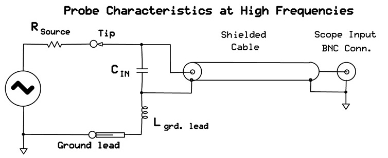
FIGURE 1B
Referring to Figure 1B, the probe appears to the circuit as shown, when probing these higher frequencies. In this region, the probe’s resistance no longer enters the picture as the magnitude of impedance is almost totally capacitive (when using a very short direct ground connection). Also, the XL of the clip tip begins to be of some significance, but even more so is the increasing XL of the ground lead attached to the probe. These two components (Cin and L ground) will form a series resonant circuit at some point which can really mess up measurements. Even the best of probes have a resonant point regardless of the grounding system used.
High-end probe designers are constantly trying to move this resonant point up higher in frequency to push it up and well outside of the passband of the equipment being used. Small values of distributed ‘L’ and ‘C’ may be inserted at key points to flatten out response and raise the input impedance, but even with the best efforts, this will only show a certain degree of improvement.
So, in light of these facts, what do we end up with here? It is evident that in high frequency circuits, the probes Xc is decreasing and loading the test circuit more. At the same time, the XL of the ground lead is increasing and, at some point, will resonate with Cin. Also, the cable ground potential at the scope end is not the same potential as the probed circuit ground at the other end due to the ground lead’s (typically 5-6”) impedance. The scope faithfully displays its input signal, however that is only the signal that appears across Cin (in Figure 1B). The probed circuit is applying its signal across both Cin and Lgrd, thus producing a volt divider action (along with some other nasty things) at the actual scope input. At some point, the signal resonates with Cin and Lgrd.
Since a series resonant circuit produces a dead short across its terminals (in an ideal world), this puts a tremendous load on the probed circuit and greatly reduces signal amplitude. Oddly enough, since each leg (L or C) has maximum current and impedance at resonance, the voltage will soar across these components causing a very high displayed screen level when in reality, the circuit’s signal level is at its lowest point.
In my experience, most 10X probes will resonate in the 70 to 110 MHz region and will be somewhat subjective to the signal source R and C values. Due to those values, the resonant point can narrow, broaden, and or have a major or minor effect on signal amplitude. The probe’s reactance can also add horrendous overshoot and ringing, along with slower rise times on displayed square waves that otherwise are not present. Three things happen when a probe is attached to a test circuit:
- The circuit’s signal is altered.
- The signal is divided and distorted at the junction of Cin and Lgrd.
- The signal sent to the scope’s vertical input will not be an exact reproduction of the signal present at the test circuit’s signal in normal operation.
The magnitude of these effects are dependant on the probe, the circuit under test, and the signal’s frequency content, making measurements quite unpredictable!
Now that we are armed with this new information, let’s go back and review the ‘problems’ we had earlier with those prototypes. First, the wide band amplifier is a simple circuit with a 300 ohm collector load. When operating at 150 MHz, the probe has a loading effect of <100 ohms Xc across that resistor. This load drops the amplifier output to 30% of what was really there. When operating with a 90 MHz signal, the probe is deep into resonance producing a much higher displayed signal than expected. Again, not really there in normal operation. Similar results are falsely displayed on subsequent stages of that proto.
In the oscillator circuit, the first point probed was in a critical feedback leg and the probe’s Cin to ground totally killed oscillations. The second point in that circuit was less critical and oscillations survived albeit with a large shift in frequency. The fast rise square waves have been slowed by the probe’s loading capacitance and ring at the probe’s resonant frequency. So, it’s bad enough that the displayed wave forms may not always follow what the probe is seeing but also, the connected probe is altering the test circuit operation. Worse yet, the results are unpredictable.
What You Can Do About the Problems
The first thing is to remove the clip tip to reduce series inductance, and use the shortest ground lead possible for the same reason. If possible, try to probe lower impedance points in the circuit to reduce loading effects. As far as probe resonances, they are most prominent at source impedances below 50 ohms, having lesser effects with source impedances above several hundred ohms.
For the low Z sources, a low ohm value tip resistor can be added to dampen the resonant point. A 1/4 watt resistor wrapped around the tip and with the other lead cut short will suffice. This resistor now becomes the ‘new’ tip. Generally, this value will be in the 50-100 ohm range.
Lastly, I do a thorough study of the circuit under test to try and predetermine the results of adding a probe to that circuit. These suggestions are a rule of thumb rather than an ideal ‘cure-all.’
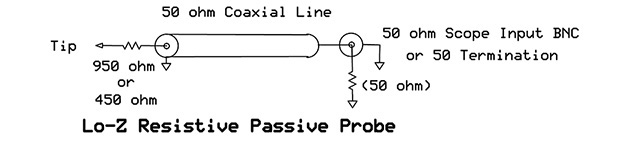
FIGURE 2A
There are two types of probes that will overcome most of these problems. One is the low Z passive probe shown in Figure 2A and the other is the active probe shown in Figure 2B. The first one is cheap and easy for home construction. It is merely a 1/4 watt carbon resistor soldered to the end of a 50 ohm coaxial transmission line with a mating BNC connector at the opposite end. The resistor leads should be cut short and act as the probe tip. The coax ground lead at that point should also be kept relatively short.
These types of probes are much more immune to ground leads effects than other probes, but when making very critical measurements, that shield should be temporarily tack soldered to the circuit’s ground.
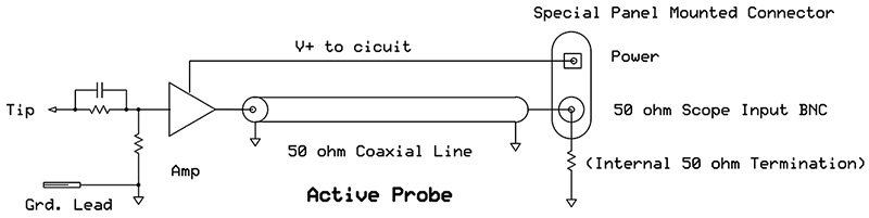
FIGURE 2B
The upside of this probe is that it is “king of the hill” for high speed probing, and has superior fidelity, very fast rise time, and very wide bandwidth. The downside is heavy loading and a high probe attenuation factor. For the two values of R shown, the attenuation is 10X with 450 ohms and 20X with 950 ohms. Also be aware that it is DC coupled. Ideally, these connect to a scope’s 50 ohm input port (which most quality scopes with >150 MHz BW have). In lieu of that, a 50 ohm termination will have to be added between the scope’s normal one meg input jack and the probe’s BNC termination.
Unfortunately, the scope’s approximate 20 pF of input capacity at this port will still be present under this situation and will present an increasing VSWR vs. frequency, skewing results above 100 MHz. In spite of this probe’s shortcomings, it has very low input capacitance (<1 pF), thereby presenting an almost purely resistive load to the circuit under test; VHF frequencies and above will actually have less loading effect than the aforementioned 10X passive probes.
As cautioned, the probe is DC coupled but is actually an advantage in standard five volt logic circuitry. In my experience, there was a 20% loading factor in probing high speed CMOS logic devices, but the fidelity is preserved and predictable.
The active probe is shown in simplified form in Figure 2B. Typically, the probe initially couples the signal through a very small coupling capacitor (although some are DC coupled through an RC network) into a high input impedance amplifier. The input network is adjusted to give a 10:1 attenuation ratio with a very small Cin (<1 pF). The amplifier will have a gain of X1 to X10. This gives the probe an attenuation ratio of anywhere from 1X to 10X. It is rare to find these probes with a 1X configuration (no attenuation).
More commonly, they will be in a 5X or 10X configuration. In all cases, the output is converted to 50 ohms Z and sent down a 50 ohm transmission line to the scope’s vertical input. The down side of these probes include the Bulky probe tip (in some models), external DC power required, limited dynamic range, and a shocking sticker price averaging $2,000 to $3,000. The highest priced one I ever saw came in just under a whopping $16,000.
Their upsides are superior bandwidth (some >10 GHz), excellent rise time, and high R/ low C probe input specs. However, these phenomenal specs do not come without some strings attached. When dealing in precise and faithful probing in the realm of microwave frequencies that these probes are capable of, the probe’s accessories and techniques become almost as important as the probe itself to insure quality results.
Depending on the probing situation, special grounding adapters have to be used and special resistive probe tips have to be interchanged (as many as a dozen or more). In some cases, special sockets have to be installed and soldered directly to the circuit board which will mate up to an accessory probe tip. Include a thorough understanding of the circuit being probed so that the correct accessories will be installed and it’s easy to see that these high-end probes are not for the amateur.
Constructing one of these probes at the hobbyist level would be very difficult to say the least. However, in spite of the shortcomings of the common 10X passive probes, they are still the workhorse of the industry and are very worthwhile for general-purpose probing. Their dynamic range far outpaces any other type probe made and often approaches upper limits of 500-600 volts. I would always include a couple in my arsenal of probes.
What I Did About the Problem
I have always been intrigued by the concepts of the low Z passive probes and active probes. After years of frustration using the common 10X passive probes, I decided it was time to switch to one of these superior probes. Since I could not justify the expense involved in a commercial product, I thought I would design and construct one myself. Each probe has its benefits and drawbacks. The low Z has excellent fidelity, rise time, and bandwidth but gives way too high loading and attenuation. The active probe also has these great features but with the added benefit of low loading and low attenuation.
However, it comes with the added burden of a bulky probe size (in my design), limited dynamic range, necessity of external power, and difficulty constructing and calibrating the input network. In mulling over the various pluses and minuses of these probes, I decided to construct a hybrid of the two, which I humorously call the “Passive-Active” probe. Figure 3 shows the completed unit.
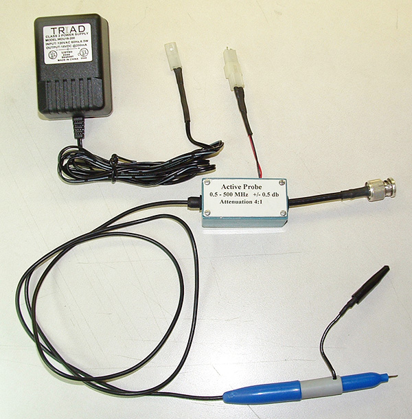
FIGURE 3
The probe starts out in the traditional low Z style with a resistive divider feeding a 50 ohm transmission line, but with one exception: a much higher input impedance (i.e., 3,400 ohms as opposed to 1,000 ohms). This is fed to an active probe’s traditional amplifier circuit before being applied to the scope’s input. The amplifier makes up for most of the divider losses. This probe still suffers some of the unavoidable consequences of its commercial counterparts, such as a limited dynamic range, moderate circuit loading, and necessity of external power.
Due to design constraints, the optimum dynamic range was determined to be 8V p-p input at its upper end with the low end of that range being 15 mV p-p input to obtain two divisions of vertical deflection (typical sensitivity for wide band scopes). This should handle the normal range of signal levels encountered in high frequency circuitry. It will not handle very low amplitude signals applicable to radio receiver circuits, but that is a job intended for spectrum analyzers only.
As to circuit loading, there really are no high impedance circuits once we enter the VHF spectrum and above. Normally, most circuit source impedances will range from 25-500 ohms at these frequencies. Even reactive LC circuitry will have much lower impedance comparable to low frequency counterparts. So, the 3,400 ohm loading factor of this probe will pose an acceptably small loading on most VHF circuitry. And more importantly, it imposes a very small reactive loading (>>1 pF).
In high frequency measurement, the probe’s reactive component is much more critical than its resistive one in terms of circuit loading (as explained earlier). Finally, as to external power, this turned out to be of little inconvenience due to the amplifier’s onboard regulator and power plug. It required only a separate wall plug transformer of adequate voltage. I leave this wall wart plugged into an outlet strip mounted on the back of my scope cart. This makes probe installation quick and easy — just one added cable to connect/disconnect.
Probe Design
In designing this probe, a number of factors had to be considered. It all starts with the MMIC (monolithic microwave integrated circuit) amplifier which has a gain of 31 db (X34), a 1 db compression point (the very onset of saturation) of 12.5 dbm (approx. 2.5V p-p), and a frequency response roll-off of -4 db at 500 MHz. It also requires a 50 ohm source and load impedance to maintain these specs, along with good stability. Best performance with these amps is obtained with a bias (B+) current of 36 mA. The B+ supplying this current ideally would be through a load resistance of infinite impedance because this load is effectively placed in parallel with the 50 ohm termination impedance. A constant current source comes to mind but will not work here as per manufacturer’s application notes.
If the bandwidth ratio was not quite so wide, a suitable RFC (radio frequency choke) could be used with a bias supply of 5 VDC. However, this circuit requires a very wide bandwidth ratio (1,000:1); no RFC would work due to their inherent self-resonance at some point, rendering them useless at frequencies above that. So, a pure resistance is required here to supply the bias current and I want that value to be as high as possible. Of course, the higher the resistance, the higher the supply voltage has to be to supply that current. A compromise had to be made here in terms of voltage, wattage dissipation, and shunt loading. I chose 18 volts which works out to 392 ohms for the supply resistor with a dissipation of 1/2 watt, without upsetting the output termination to a great degree.
Given that 392 ohms is not the ideal value here, the amp’s maximum output level is degraded, so I decided to spec that figure at +10 dbm (2.0V p-p) for best linearity. Given the amplifier’s gain with a 1:1 attenuation ratio, this would only allow for a max probe input impedance of 850 ohms and its dynamic range limited to 2.0V p-p on the upper end. These limits just would not satisfy a wide range of probing situations, but by increasing probe attenuation to 4:1, I could get the 8V p-p input level I was after at the upper end of range, and increase the input impedance to 3,400 ohms. The actual input impedance works out to 3,400 ohms shunted by <<1 pF. This provides an acceptable loading factor while maintaining the desired dynamic range.
It now becomes a 4x probe and it is easy to calculate the actual display amplitude vs. input signal amplitude — just double the displayed voltage and double it again (X4). Not as easy as a 1X or 10X probe, but still quite simple to compute in one’s head. The amplifier roll off, cabling connections, and board layout combined will add up to a little less than a -6 db (2x) loss at the upper limit of 500 MHz of the probe’s bandwidth, so the next problem to be solved was how to flatten this response curve. The straightforward answer was to shunt R1 and R2 with a compensation capacitance. The Xc needed for this compensation worked out to be 2,000 ohms at 500 MHz which has a value of 0.18 pF.
It worked out in my favor on this one due to the fact that 1/4 watt carbon film resistors have a parasitic capacitance of 0.35 pF. Two in series would give me 0.175 pF — almost exactly what I needed! A call to KOA Speer’s (resistor manufacturer) engineering department confirmed that these resistors are made to exacting mechanical tolerances and that the parasitic is uniform from unit to unit with one minor exception. The laser etching used in the manufacturing process is slightly different from one group of values to the next; a group value being a certain range of resistance in perhaps a 5:1 ratio.
Next I needed to pick out two values of resistance that would give me a combined value of 3,400 ohms and a parasitic capacitance of approximately 0.175 pF. The values chosen were accomplished empirically due to the fact that the exact capacitance could not be predetermined. After considerable experimentation, a set of values was found to be 1,000 ohms in series with 2,400 ohms, with the correct parasitic capacitance to flatten out the response curve.
To confirm what the manufacturer told me, I tried out several sets of these and got identical results. I also tried out some others from different manufacturers and the results were very close. Just to be on the safe side though, stick with the numbers in the Parts List. The final specs on the probe work out to this:
- Attenuation ratio: 4:1 (4X probe)
- Frequency response: 0.5 to 500 MHz ±0.5 db
- Maximum tip input: 8V p-p
- Input impedance: 3,400 ohms - 0.2 pF
- Probe tip impedance: 3,400 ohms - <0.5 pF
- Rise time <500 pF
- -3 db point >750 MHz (estimated)
- Resonance: >I GHz (estimated)
Probe Construction
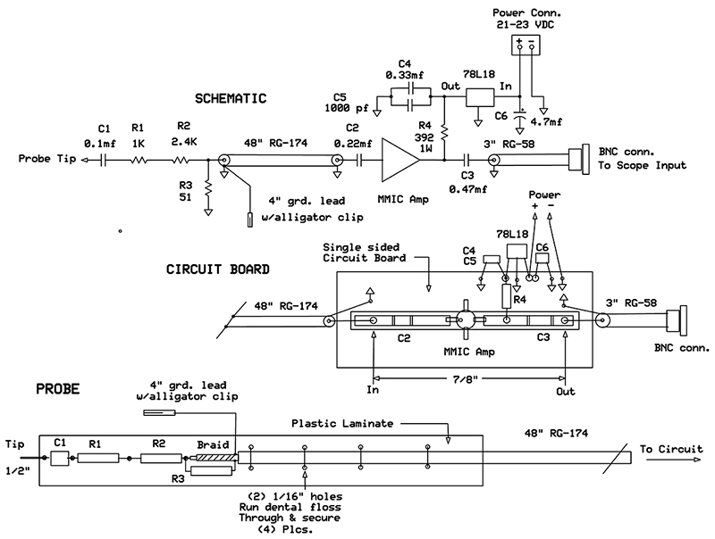
FIGURE 4
The construction of this probe is quite simple and low cost. I had an old Pomona box laying around that I used for the active board enclosure. The cables came out of my junk box and were cut to proper length. I paid $20 for the remaining parts needed. The wall plug transformer was the most expensive at $10. The probe components are installed in a modified Sharpie felt tip pen housing. The cap was removed and the pocket clip snipped off flush with the body. Then, a 1/8” hole was drilled into the end to accept the RG-174 cable. I then removed 1” of material from the end of the pen body, reached in with needle-nose pliers, and removed the ink cartridge.
The protruding felt tip was then snipped flush with the end of the body. I stood the body up straight on a firm surface and got the remaining felt out by driving it back into the housing with a hammer and punch (a flat end nail of the proper size will also do). A little cleanup work was needed inside the housing, so I used various drill bits and rotated them by hand to remove the remaining plastic nibs. The housing will need a thorough cleaning to remove any remaining ink residue; the process can be a bit messy.
I used a piece of plastic laminate (Formica) shaped to fit the interior all the way to the tip. Although Figure 4 shows this as a rectangular shape for drawing simplicity, the finished piece will be more bullet shaped near the tip end. The components C1, R1, R2, and R3 are all thru--hole components. Since a copper-clad board has too much stray capacitance, these parts lend themselves to better support in this application.
After I was satisfied I had a good fit in the housing with the laminate, I pre-drilled all the mounting holes. The actual probe tip was a broken needle from my wife’s sewing machine and it takes solder quite readily. This was soldered to one lead of C1 with its other lead dropped through its board hole and yanked back to hold it in place. The probe tip is then positioned on center with about 1/2” exposed beyond the laminate. A blob of epoxy cement is dropped on it to preset it.
When cured, another blob is smeared over it again and half of C1, and is allowed to flow around both sides of the board. This gives the tip adequate support when cured. The component leads are dropped through their corresponding holes; their leads bent back and joined with a healthy dose of solder. When cooled, snip these flush with the board. The exposed section of the cable braid is actually pinched back to form two solder nibs where R3 and the ground lead connect; then get it pre-tinned.
Attach the RG-174 cable and secure it down with dental floss (the waxed type is best). Drill a thru-hole in the probe body at an appropriate spot for the ground lead to protrude. Push the ground lead through it from outside the housing and far enough so that the protruding end sticks out far enough to allow soldering to the cable’s ground braid when the probe board is partially inserted into the housing. When completed, the probe board is pushed in all the way until it is snug.
Apply a slight pulling force on the ground lead while doing this. There should be about 3/8” of probe tip protruding from the housing end. In my probe, friction was all that was needed to keep it in place. Some wadded, non-conductive material would have been jammed into the open end had this not been the case.
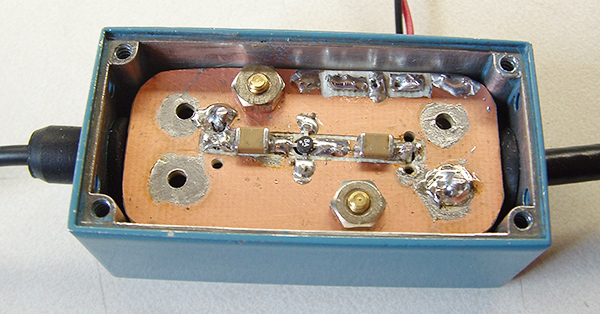
FIGURE 5
The back of the probe body needed a little abrading to accept the cap with a nice snug fit. The finished active circuit is shown in Figure 5. This circuit starts out with a piece of 1” x 2” single-sided copper-clad board. A trace 3/16” wide x 1-1/4” long was etched right down the center of it. A couple of small islands were also etched out at the upper right corner to accept the regulator (TO-92) and its associated components.
On the long trace, a 1/8” hole is drilled where the MMIC amplifier will reside. This is located about 1/4” off center to the left along the axis of that trace. The remaining copper area at the edge of the hole was then removed to completely break the trace’s path. Also, two breaks were etched out where the chip capacitors will be installed. (A note here: When I refer to etching, I mean etching with a rotary tool, knife, or whatever.) The remaining thru-holes were drilled and the remaining components were mounted. R4, C4, 5, 6, and the regulator are all thru-hole components and mounted from the other side of the board (phenolic side). The R4 lead length is not critical, just make sure it fits.
The MMIC amp has one tapered leg with a corresponding color dot on its case — this is the RF input terminal. This was then soldered into place along with the two chip capacitors C2 and C3. Depending on the enclosure used, the cable installation will vary. In my case, the cables pass through grommeted holes in each end, and were pushed through the enclosure before soldering them to the circuit board. In prepping the cable ends, keep these leads short.
Expose only about 1/8” of insulation on the center conductors. Twist the braids to form a wire for the ground lead, then push these leads into their corresponding holes and solder them to the board as close as possible. Ideally, there will only be about 1/8” of exposed wire/insulation at these connections. After all the soldering was completed, the board was secured to the enclosure on two pre-installed 1/2” standoffs. One final comment about overall construction — plan ahead and after every machining operation, make sure the respective parts fit as intended before proceeding with soldering.
Add the final power leads, connectors, etc., and the probe is ready to use. A word of caution here: Double-check all connections and polarities before initial power-up as the MMIC amp operates at 4 VDC and will not tolerate reverse polarity when fed from an 18 volt supply.
Testing the Probe
For a simple circuit, this probe required many dozens of tests throughout its design cycle to verify performance vs. circuit changes, so it came as no surprise to me that the finished unit operated as expected. In that cycle, various ground lead lengths of 1” through 6” were tried with only small changes in performance. Even though ground leads degrade performance somewhat, I wanted one for convenience of use. After some consideration, 4” was the best compromise and the circuit was optimized for that. This works because the low Z style probe is much more immune to ground lead problems than other style probes.
With everything completed, the probe should work as advertised, but I still ran a battery of tests with capable test equipment to verify that. Upon completion, it would be reassuring if you could do the same even if you had to temporarily beg, borrow, or steal the necessary equipment to do so. One thing I want to point out here is that the probe has a 50 ohm output impedance and will perform best with scopes that have a 50 ohm vertical input port (most scopes having >150 MHz BW have this port).
In lieu of this port, there are 50 ohm BNC/BNC terminations available that can be attached to the standard 1 meg vertical input jack. Bear in mind that using that input, there will be an increasing VSWR with increasing frequency due to the scope’s 20 pF of input capacitance at that jack. So, displays will be somewhat skewed above 100 MHz.
Upon completion of this probe, I ran side by side comparison tests against a variety of my common 10X passive probes. The tests were performed on a variety of commercial circuits that had known and documented signal levels at various frequencies from 10 to 500 MHz. The passive probes performed well up to 10 MHz and fair up to 25-30 MHz on most circuits, but not all. Once I entered the VHF region (30 -300 MHz) all bets were off as the CRT displays were becoming erratic and unpredictable.
At times, they registered only 20% of the actual amplitude level and at other times, the levels were much higher than the true levels. By comparison, the active probe performed very well in all circuits probed, giving a very close display to all documented levels. It only produced a small frequency shift ( <1%) in sensitive areas of oscillator circuits as compared to the 10X probe (>8%). Also, the loading was quite good to acceptable in these circuits, but that loading was also quite predictable (i.e., 330 ohm collector load - 3,400 ohm probe Z - 10% loading).
The 3,400 ohm probe impedance may seem alarmingly low to you and it well may be for low frequency circuits, but this probe is designed for high frequency circuits above 20 MHz where source impedances tend to drop dramatically from lower frequency circuits. So, it’s not as bad as it first appears — in spite of the fact that the probe’s impedance reduces further yet at higher frequencies. Consider that this probe has an input R of 3,400 ohms paralleled by 0.2 pF which would yield an input impedance of 2,100 ohms at 300 MHz. The common 10X probe has an input R of 10 megohms paralleled by 12 pF. The 10 meg has no effect as the input is purely capacitive at this frequency, yielding an input impedance of 45 ohms; it gets worse as the frequency goes up.
The active probes impedance looks quite stiff by comparison. The rise time on this probe is excellent but unfortunately since this probe is AC coupled by necessity, it can only handle square waves above a few hundred kHz; increasing the coupling capacitor values would improve this, but there are limits.
Probing Tips and Thoughts
After using this active probe for a while, I have gained complete confidence in it and it has opened up a whole new world of investigation for me. It has also answered many unaccountable readings encountered in testing previous circuits that had mysterious operations. When using this probe (as well as any other probe), good high frequency techniques require that the probe cable be free of kinks and kept clear of the circuit under test.
The probe tip should enter the test point perpendicular to the circuit board. Always grasp the probe near the cable end so as to minimize finger presence at the probe tip. Once again, I want to stress that the common 10X passive probe is the workhorse of the industry and a valuable asset to your collection of probes. But you must be aware of the fact that for other than general probing at high frequencies, many false readings will occur with it.
If you decide to build this probe, visit www.koaspeer.com. It has a wealth of information in its application notes, along with case outlines and demo board layouts for the MAR-8 MMIC amplifier. There’s also good info on a lot of their interesting products. NV
Active Probe Parts List
| ITEM |
DESCRIPTION |
|
| C1 |
O.1 MFD/50V MLC ceramic |
|
| C2 |
0.22 MFD/50V chip size 1812 |
|
| C3 |
0.47 MFD/50V chip size 1812 |
|
| C4 |
0.33 MFD/50V MLC ceramic |
|
| C5 |
1,000 pF/50V MLC ceramic |
|
| C6 |
4.7 MFD/50V tantalum electrolytic |
|
| R1 |
4.7 MFD/50V tantalum electrolytic |
|
| R2 |
2,400 ohm 1/4W carbon film |
|
| R3 |
51 ohm 1/4W carbon film |
|
| R4 |
|
|
| MMIC |
MAR-8A mini-circuits |
|
| 18V Regulator |
78L18 |
|
| Wall plug |
|
|
| Power Pack |
Triad 18V/300 mA |
|