Recap
In our last episode, we finished looking at the AVR memory architecture and wrote a bootloader that lets us upload programs to an AVR without having an external programmer. One of the things we learned in the memory series is that the AVR was designed around Flash EEPROM for program memory. Flash memory is great stuff and you probably have a few billion bytes of it in the form of media cards sitting around in odd places like your cell phone, digital camera, or music player. In addition to the ubiquitous media cards, Atmel has a family of ICs called DataFlash that allow you to use Flash in your circuit designs. Both the media cards and the DataFlash have something in common: they can be written to or read from using the SPI (Serial Peripheral Interface) bus which is probably the simplest serial communications protocol around.
In the next few Workshops, we will progress to using external Flash memory via SPI, but first we will learn about shift registers which lead logically to SPI. The shift registers we are using could be used with AVR hardware SPI, but we will first write our own software to use our shift registers mainly to show how easy it is and to help understand how these things work. We will look at the 74HC595 eight-bit serial-in-parallel-out and the 74HC597 eight-bit parallel-in-serial-out ICs. [We could also use the 74HC164 74HC165 pair, but the boat left the dock before I realized I had those lying around.] Finally this time, we will apply these chips to create yet another Cylon Eyes display, but this time we will have 16 LEDs to sweep and a full eight-bit DIP switch to allow the user to change the LED patterns. Instead of having to use 24 pins as we would if we did this parallel, we only use four of our AVR I/O pins.
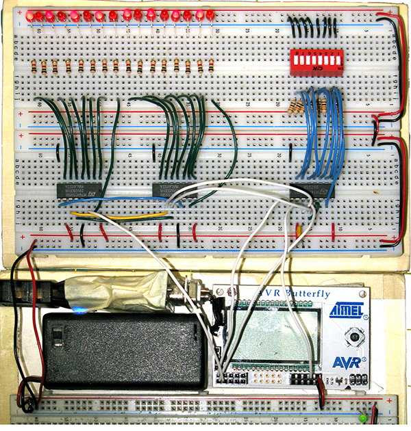
FIGURE 1. Butterfly with Shift Registers.
As a bonus, we will do all this on four different development platforms. Figure 1 shows things wired up with the Butterfly, and Figures 10, 11, 12, and 13 show the soft SPI pins so that you can use any of these devices: the Butterfly (Workshop 1), the Arduino (Workshop 9), the Breadboarduino (Workshop 21), or the BeAVR40 (Workshop 22) to do the experiments this month.
Shift Registers
If you’ve had the good fortune of taking a college level course in digital logic, then you already know a lot about shift registers and their basic element: the flip-flop. These circuits are fundamental to the entire digital revolution and if you want to really understand how all your digital electronic servants work, you are going to need to understand these guys. Since our goal at this point is just to use them, I’ll leave the gory details to your Google self-education program and glide over the fundamentals.
A flip-flop is a circuit that can remember a bit state; either 0 or 1. The most common type of flip-flop is the D or delay flip-flop that records the input bit state on the rising edge and puts that value on the output on the falling edge. Prior to the falling edge, the output is the previous bit state. The rising or falling edge allows us to create a serial shift register with D-type flip-flops arrayed in a sequence such that each input records the prior flip-flop’s output on the rising edge, then puts that value on its output on the falling edge.
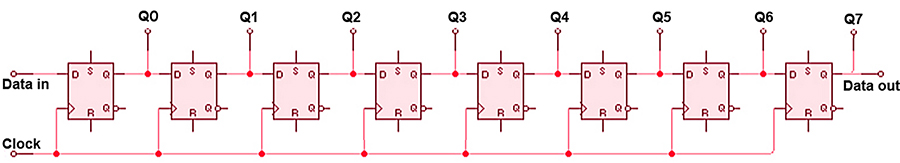
FIGURE 2. Flip-flop Shift Register.
This is shown in Figure 2. [Caveat: Not all flip-flops work exactly the same.] You could do this equally well by having the reverse clock logic if the design calls for it. Each of the flip-flops will also have a clear pin so that you can set them all to 0 at once. When you string eight flip-flops together, then you consider the input of the flip-flop on one end as the serial in pin for the shift register and the output pin on the flip-flop on the other end as the serial data out pin. The Q# pins on each flip-flop hold the full eight-bit data state and can be read or written to for parallel I/O.
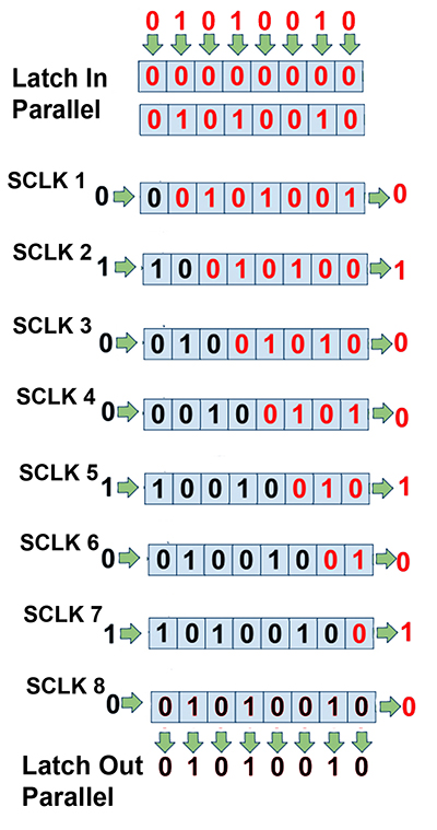
FIGURE 3. Shift Register Concepts.
Figure 3 shows a parallel byte of data — Q0 to Q7 — being latched into the register, then shifted out one bit at a time for each clock pulse while a new bit is clocked in. Unfortunately for Figure 3, I chose the same byte value (0x52) for both the parallel and serial I/O, and though it might have made a bit more sense to illustrate this with two different bytes, hopefully you’ll still get the general idea.
Suggested Resources
If you want further information on shift registers, I suggest you read the Wikipedia sections on flip-flops and shift registers. If you want to REALLY understand these things, get the book Code by Charles Petzold. He starts with mechanical relays to recreate digital logic elements that could have been built in the 19th century and shows how the fundamental computer concepts could have been implemented even back then. His approach helps separate the ideas from the implementation which really helps you understand how to make logic machines.
Serial-In-Parallel-Out Shift Registers — the 74HC595

FIGURE 4. 74HC595 Pins.
The ‘595 — whose pin-out is shown in Figure 4 — is an eight-bit serial-in-parallel-out shift register IC available in a 16-pin DIP package [www.nxp.com/documents/data_sheet/74HC_HCT595.pdf]. The outputs can be in one of three states: VCC, GND, or disconnected (high impedance). You can clear the register by toggling the /MR, and you can shift out data at 100 MHz. There are two registers: one for shifting serial bits and one for buffering the parallel output pins. Each register has its own clock; the serial being clocked by the SH_CP pin and the parallel by the ST_CP pin. Both transfer data on the rising edge of the clock. Figure 5 shows how bits are clocked into this device.

FIGURE 5. 74HC595 Timing Diagram.
We use the 595 by presenting a bit of data on the serial data input pin 14 (DS) and then toggling the shift register clock input pin 11(SH_CP) as shown in Figure 5. We do this for the eight bits that we want to shift into the register, then we toggle the shift register clock input pin 12 (ST_CP) to cause the 595 to move the data from the serial shift register to the parallel output register. We can hook these in series so that the serial data output line pin 9 is connected to the next 595’s serial data input pin 14 (DS). The only difference is that we shift in 16 bits instead of eight as with the single 595.
Parallel-In-Serial-Out Shift Registers— the 74HC597
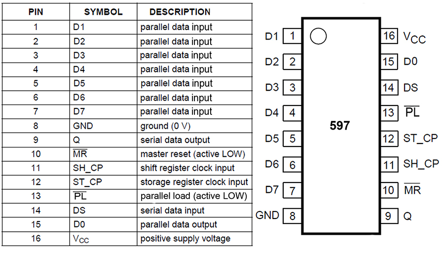
FIGURE 6. 74HC597 Pins.
The 74HC597 (whose pin-outs are shown in Figure 6) is sort of the sister chip to the 595 in that it reverses the process. It adds one non-SPI control line that is required to load the data from the parallel pins to the shift register before clocking the data out. For our purposes, we hook this line to the ST_CP line so that we latch bits and load bytes in one operation which doesn’t seem to hurt anything [http://www.nxp.com/documents/data_sheet/74HC_HCT597.pdf].
Using the 74HC595 — Control 16 LEDs
Figure 1 shows a bit of a rat’s nest of wires on breadboards. The two ICs on the left are 595s and are used to control the 16 LEDs. The schematic for this is shown in Figure 7, but please note that this doesn’t show the IC VCC and GND connections with pins 14 and 8, respectively. Since our goal is to get some preliminaries on SPI, I’ve named the pin signals with their SPI equivalents.
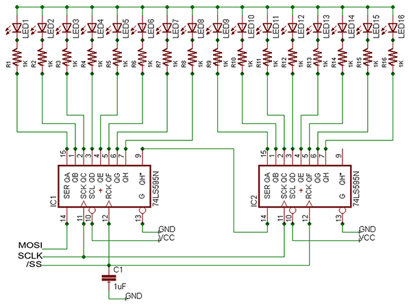
FIGURE 7. Serial-In-Parallel-Out Schematic.
In our software, we need to do several things to send out the 16 bits of serial data and have them show up on the two 595 outputs. First, we set the /SS (Slave Select) to 1 so that the bits will not show on the parallel output while they are being shifted into the devices (this locks the old data on the output until all the new data is input). Next, we present each of the 16 bits in sequence on the MOSI (Master Out Slave In) pin, followed by toggling the SCLK (Serial CLocK) pin that tells the 595 to shift that bit into the serial register. Finally, after all 16 bits are shifted in, we set the /SS low which causes the serial bits in the serial shift register to be transferred to the parallel output register. The following code snippet shows how to turn on every other LED:
// Set alternate LEDs on off<br />
// 0x5555 HEX <> 0101010101010101 binary<br />
Uint16_t myVar = 0x5555;
// Clear slave select so data won’t show while shifting<br />
clear_ss();
// output 16 bits to the 595<br />
for (i=0; i<=15; i++)<br />
{<br />
    // Put bit on mosi_pin<br />
    if(is_bit_set(myVar, i)<br />
        set_mosi_bit();<br />
    else<br />
        clear_mosi_bit()
// Toggle the clock to output it<br />
toggle_clock();<br />
}
// Set slave select to transfer data<br />
// from serial to parallel registers<br />
set_ss();
Since our purpose at this point is to get the 595 working, we’ll defer looking at the SPI macros in the code snippet (hey are in the source code).
Using the 74HC597 — Read an eight-bit DIP Switch
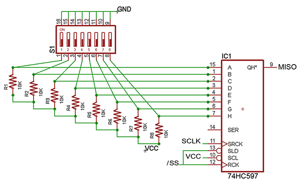
FIGURE 8. Parallel-In-Serial-Out Schematic.
We will test this IC using the circuit shown in Figure 8. We use the 597 by first toggling the storage register clock input pin 12 (ST_CP) to shift the parallel port input pin states (D0-D7) to the parallel register. Next, we toggle the parallel load line pin 13 (/PL) which causes the 597 to move the data present in the parallel input register to the serial shift register. Finally, we toggle the shift register clock input pin 11 (SH_CP) eight times to shift the bits out on the serial data output pin 9 (Q) which we monitor with our MISO (Master In Slave Out) pin. We can see this process in action in the following code snippet:
Code Snippet:
uint8_t my_data_in = 0;
// Clear slave select<br />
// so data won’t show while<br />
// shifting<br />
clear_ss();
// load 8 bits from the 597 into<br />
// my_data_in byte<br />
for (i=7; i>=0; i—)<br />
{<br />
// Toggle the clock to get the<br />
// next bit<br />
        toggle_clock();
        // If data pin = 1 set it<br />
    // in my_data otherwise<br />
        // do nothing since my_data_in is<br />
    // initialized to 0<br />
        if (get_miso_bit())<br />
            my_data_in |= (1 << i);<br />
        uart_send_bit(1);<br />
        }<br />
    else<br />
    {<br />
        uart_send_bit(0);<br />
    }<br />
}
// Set slave select to transfer data<br />
// from serial to parallel registers<br />
set_ss();
This snippet is part of Shift_Register.c code that you can get in the Workshop28.zip from Nuts & Volts. When you set the DIP switch to 0xAA (binary 10101010), run the program while communicating with Brays terminal, and move the lowest bit from 0 to 1 you get the output shown in Figure 9.
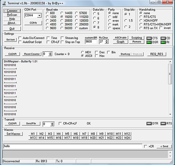
FIGURE 9. Output of ShiftRegister.C in Brays Terminal.
Software SPI Pins
SPI uses four pins: MOSI, MISO, SCLK, and /SS. For us to use these in software, we must designate specific pins from specific ports and then we must set them up for data direction (input or output). While any pins common to all the boards we are writing our code for would be okay to use, we will define the following:
#define mosi_port PORTB<br />
#define mosi_port_pin  PORTB2<br />
#define mosi_ddr  DDRB<br />
#define mosi_port_pins PINB
#define miso_port PORTB<br />
#define miso_port_pin  PORTB1<br />
#define miso_ddr  DDRB<br />
#define miso_port_pins PINB
#define sclk_port PORTD<br />
#define sclk_port_pin PORTD7<br />
#define sclk_ddr DDRD
#define ss_port PORTB<br />
#define ss_port_pin  PORTB0<br />
#define ss_ddr  DDRB
We then set the data direction as follows:
void setup_pins()<br />
{<br />
      // Initialize MISO as input<br />
      // set DDR pin register to 0<br />
      miso_ddr &= ~(1<<miso_port_pin);
      // Initialize MOSI, SCLK, AND /SS as outputs<br />
      // set DDR pin registers to 1<br />
        mosi_ddr |= (1<<mosi_port_pin);<br />
    sclk_ddr |= (1<<sclk_port_pin);<br />
      ss_ddr |= (1<<ss_port_pin);<br />
}
If the way I’m setting or clearing bits isn’t clear from earlier Workshops, then I highly recommend that you refer to a tutorial: [TUT] [C] Bit manipulation (a.k.a., “Programming 101”) located at: www.avrfreaks.net/index.php?name=PNphpBB2&file=viewtopic&t=37871. This will also help when you look at the source code.
I’ll admit to getting confused trying to remember which pin represented which signal so that I could properly connect my software SPI signals from each of the platforms to the 595 and 597. To help with this, you can refer to Figures 10, 11, 12, and 13, which show the Butterfly, Arduino, Breadboarduino, and BeAVR40, respectively, with the soft SPI pins labeled.
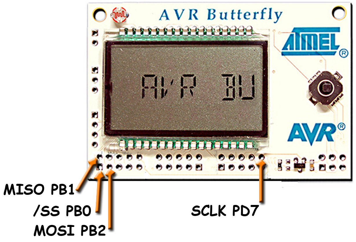
FIGURE 10. Butterfly Soft SPI Pins.
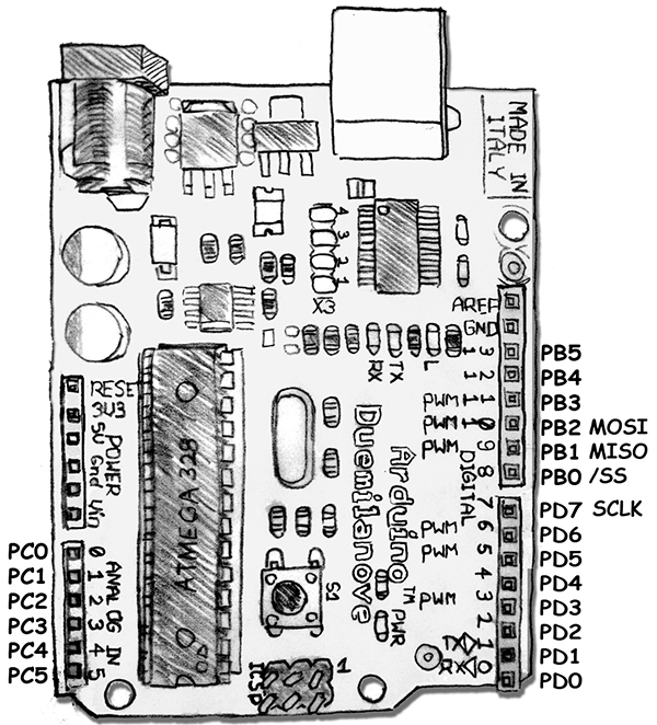
FIGURE 11. Arduino Soft SPI Pins.
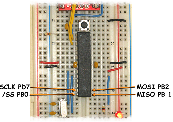
FIGURE 12. Breadboarduino Soft SPI Pins.

FIGURE 13. BeAVR 40 Soft SPI Pins.
Yet Another Cylon Eyes Project
Figure 1 shows the circuit being controlled by an AVR Butterfly, but the source code is written to run on any of the devices shown in Figures 10, 11, 12, or 13. The full program has a bunch of sweep patterns and speeds selectable from the DIP switch, but here we’ll look at an excerpt snippet that shows how the plain old Cylon Eye sweep is run. We first create an array of values that will sweep the lit LED from right to left and then we run that array forward and backward as shown:
/*<br />
To create a 16 LED Cylon Eye effect<br />
output this array 0 to 15 then 15 to 0<br />
0000 0000 0000 0001 == 0x0001
0000 0000 0000 0010 == 0x0002<br />
0000 0000 0000 0100 == 0x0004<br />
0000 0000 0000 1000 == 0x0008<br />
0000 0000 0001 0000 == 0x0010<br />
0000 0000 0010 0000 == 0x0020<br />
0000 0000 0100 0000 == 0x0040<br />
0000 0000 1000 0000 == 0x0080<br />
0000 0001 0000 0000 == 0x0100<br />
0000 0010 0000 0000 == 0x0200<br />
0000 0100 0000 0000 == 0x0400<br />
0000 1000 0000 0000 == 0x0800<br />
0001 0000 0000 0000 == 0x1000<br />
0010 0000 0000 0000 == 0x2000<br />
0100 0000 0000 0000 == 0x4000<br />
1000 0000 0000 0000 == 0x8000<br />
*/
uint8_t i = 0;<br />
uint16_t ce[] = { 0x0001, 0x0002, 0x0004, 0x0008, 0x0010, 0x0020, 0x0040, 0x0080, 0x0100, 0x0200, 0x0400, 0x0800, 0x1000, 0x2000, 0x4000, 0x8000 };
// Sweep right to left<br />
for (j=0; j<=15; j++)<br />
{<br />
// Clear slave select so data won’t show while shifting<br />
clear_ss();<br />
// output 16 bits to the 595<br />
for (i=0; i<=15; i++)<br />
{<br />
    // Put bit on mosi_pin<br />
    if(is_bit_set(ce[j], i)<br />
        set_mosi_bit();<br />
    else<br />
        clear_mosi_bit()
// Toggle the clock to output it<br />
toggle_clock();<br />
}<br />
// Set slave select to transfer data from serial to parallel registers<br />
set_ss();<br />
// Wait a while<br />
_delay_ms(100);<br />
}
To sweep the LED back, just run the ‘for’ loop backwards as shown in the source code.
Last Shift
Well, shift registers are a pretty cool way to save microcontroller pins, but in case you’ve forgotten, all this is in preparation so we can learn hardware SPI and use it to read external Flash memory. We’ll continue in that direction next time. In the meantime, if you want to get a leg up on this you can purchase my book C Programming for Microcontrollers along with a projects kit from Nuts & Volts. If this seemed a bit dense, then you might want to try my book An Arduino Workshop, also available from Nuts & Volts. NV
Downloads
Smileys Workshop 28 Source Code