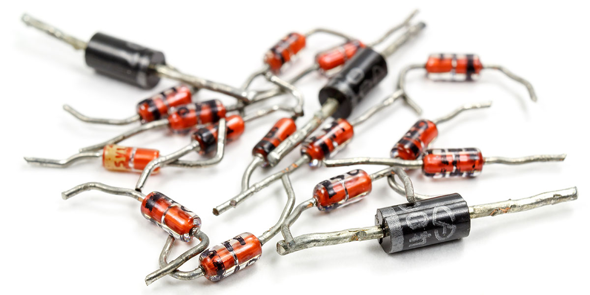
When I pick a zener diode from my parts cabinet, I always want to check its breakdown voltage before I use it in a project — just to be sure there wasn't a mix-up in my cabinet drawer. This procedure needs to be repeated when putting unused diodes back into my cabinet, or when sorting among a bunch of diodes I picked up at a surplus outlet.
It's time consuming to set up a power supply and voltmeter, select a series resistor to limit current, and measure the voltage for each diode. Alternatives like reading the part number and looking it up, or setting up a curve tracer aren't any faster. Many errors, burned out diodes, and damaged projects have convinced me there must be a better way. While experimenting with self-oscillating switching power supplies for another application, it dawned on me that this technology was the answer to my problem.
The tester described in this article is a simple two-transistor circuit operating from a 9V battery which tests zener diodes with breakdown voltages up to 52 volts. Nothing more than a multimeter is necessary to build, test, and use the circuit. Its transformer-coupled design adjusts the output voltage automatically to the voltage of the zener diode under test, while adjusting diode current to preserve a relatively constant diode power throughout the measurement range.
There’s no need to select a current-limiting resistor. Just connect a voltmeter across the diode and measure its breakdown voltage at a consistent and safe power level. The circuit will also safely test LEDs — including white LEDs that multimeters can’t test and other low voltage diodes in their forward direction, as well as MOVs (metal-oxide varistors) and other protective devices with higher voltage breakdowns.
Connecting an external power supply to the tester allows devices that break down well above 50V to be tested easily, also. With all my projects and the numerous uncharacterized devices lying around my shop, this zener tester has proven to be the most regularly used equipment on my bench!
Zener Diode Background
If you’re not familiar with zener diodes, then an introduction is appropriate. Zeners are so useful they should be found in every experimenter’s component collection. The zener diode is a specialized silicon diode that looks like a normal silicon diode in the forward direction. However, in the reverse voltage direction, it exhibits a low leakage current like a normal diode until a voltage — the so-called “zener voltage” — is reached. At that point, it sharply exhibits a controlled constant breakdown voltage despite increasing current.
All diodes start to heavily conduct at some voltage in the reverse direction, but are operated well below this breakdown voltage to avoid damage. Zeners, on the other hand, are designed to be operated in their breakdown region, and that breakdown is carefully engineered for specific voltages. For example, the 1N4728 to 1N4764 family of zener diodes includes breakdown voltages from 3.3 volts to 100 volts in 37 steps — a much broader range than common fixed-voltage three-terminal IC regulators. These diodes can also be put in series to achieve almost any voltage desired, and different diode families come in various wattage ratings from 200 mW to over 10W.
Zeners are commonly used as voltage regulators, reference-voltage standards for op-amp designs, and as protection devices to safeguard components from over-voltage conditions. Applications like relay or solenoid drivers and switching power supplies — like the one described in this article — commonly use zeners for protection (like D2 in Figure 1).
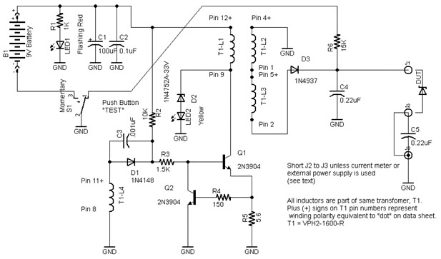
FIGURE 1. Tester schematic.
They also find use (instead of a simple series resistor) in dropping one voltage down to a lower voltage, and in clipping AC voltage waveforms. They are even used as noise generators in RF impedance bridges. Best of all — particularly for experimenters on a budget — typical low power zener diodes cost just pennies each.
The Zener Diode Tester
The diode to be tested is connected between the red and yellow terminals, and the voltage is read across these terminals when the pushbutton is depressed to test. Connecting a current meter between the yellow and black terminals allows current measurement while testing if desired, or replacing the current meter with an external power supply allows extending the tester’s range to well above 52 volts.
A flashing red LED indicates when voltage is present across the test terminals. A yellow LED indicates that the output is at the limit of 55V. When no diode is present or the zener diode has a breakdown voltage above 55V, this LED is illuminated. The LED also indicates correct functioning of the internal circuit for initial testing and serves as a safety reminder that a potentially dangerous voltage is present across the output terminals. When the test switch is released, the output is quickly discharged to zero volts for safety.
The internal circuitry of the tester is easily modified and simulated to change the voltage range or for use in other applications. These modifications and simulation are discussed later in this article.
Circuit Description and Operation
The schematic of the tester is shown in Figure 1. The key to operation and building ease is the use of a transformer, T1, which is readily available from multiple distributors and designed for use in small switching power supplies. T1 has six independent and identical polarized windings of which four are used in the tester: T1-L1 is the “primary” driving the “feedback” winding, T1-L4, and storing energy in the transformer’s magnetic field; then T1-L2 and T1-L3 are connected in series to form the “secondary,” discharging the stored magnetic energy into the diode under test (DUT).
Some of you will recognize this basic circuit as a simple “blocking oscillator,” widely used with vacuum tubes for radar applications in WWII, and later adopted as a transistor configuration for the earliest generation of solid-state switching power supplies. In the power supply realm, it’s now termed a “flyback” circuit, harking back to CRT-based/TV horizontal-output circuits using this topology, or often referred to as a “boost” circuit. It’s simple, works with many different transistors, and doesn’t require specialized integrated circuits.
S1 is an SPDT momentary pushbutton switch. Until S1 is pushed, the 9V battery is disconnected from the circuit, and output filter capacitor, C4, is discharged through R8. Pushing S1 to the ON or TEST position removes R8 from the output, and applies 9V to the primary, T1-L1, and to the start-up resistor, R2. It also turns on LED1 — a flashing red LED that indicates to the user that the circuit is energized and there are potentially dangerous voltages across the output terminals.
Start-up current flows through R2 (and R4), turning on drive transistor, Q1. As Q1 turns on, it pulls pin 1 of T1 toward ground which, in turn, causes the voltage across the feedback winding of T1/T1-L4 to rise from ground toward +9V, since the turns ratio of the two windings is 1:1. The rising voltage across T1-L4 is conveyed to the base of Q1 through C3, D1, and R3. This current adds to the current through R2, further turning on Q1 and rapidly driving it into saturation.
In the saturated state, the voltage across Q1 is a few tenths of a volt and almost the full 9V battery voltage is across T1-L1. Now, the current through T1-L1 and R6 begins to ramp up, storing magnetic energy in the core. No current flows through D3 since it’s reverse-biased during this part of the oscillation cycle.
When the voltage drop across R6 rises above 0.7V, the “choke” transistor, Q2, begins to turn on and shunt the base current of Q1 to ground, forcing Q1 to come out of saturation and the voltage at Q1’s collector to rise. This action reduces the voltage across T1-L1, which correspondingly drops the voltage across the feedback winding, T1-L4, further reducing base drive to Q1 and shutting Q1 off rapidly through this regenerative action.
When Q1 comes out of saturation and begins to shut off, the voltage at its collector rises rapidly due to inductive action, and the voltage across T1-L1 reverses, driving Q1’s collector voltage above 9V. At the same time, the secondary voltage reverses and D3 starts to conduct.
When the stored energy in the core is fully released through the secondary, the voltages on all windings collapse, turning on Q1 again via C1 (the voltage at pin 11 goes from a negative voltage toward ground). Then the cycle repeats until C2 is charged to a voltage level where the DUT begins to conduct, at which point the oscillation stabilizes and continues to feed power into the DUT.
Steady-state oscillation waveforms are diagrammed in Figure 2.
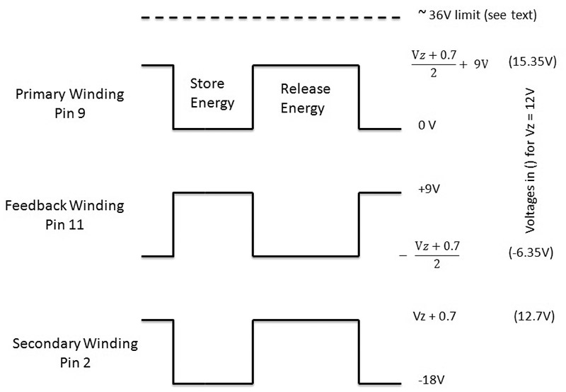
FIGURE 2. Timing diagram showing transformer voltages.
Voltage levels (referenced to ground) are shown for a generalized zener diode voltage, Vz, under test. The voltages shown in parentheses are for a 12V zener diode as the DUT, and corresponding actual circuit waveforms are shown in Figure 3.
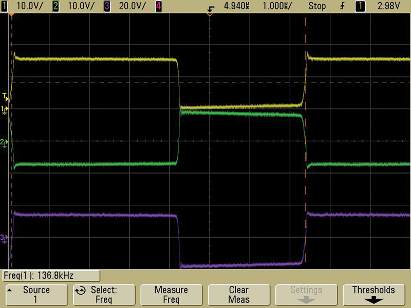
FIGURE 3. Oscilloscope capture of actual circuit testing a 12V zener.
If no DUT is present when the circuit is operating, then the voltage across C4 will continue to rise, as will the peak voltage at the collector of Q1. The voltage at pin 2 of T1 and the output voltage would keep rising with each cycle, as would the peak voltage (half the output voltage plus 9V) at the collector of Q1. This is a feature of a flyback circuit configuration, which allows zener diodes to be tested well above the battery voltage of 9V.
However, some protection is necessary to keep the peak voltage at Q1’s collector from exceeding its maximum collector voltage rating of 40V. The series combination of zener diode D2 and yellow LED2 provide this protection by limiting the peak voltage and absorbing the energy of T1’s magnetic field if no DUT is present, or if the DUT breakdown voltage is greater than the tester’s maximum output voltage. LED2 lights when there’s current through D2 in this condition.
Figure 4 shows actual measurements of current and power for various DUTs on the tester as constructed. Measurement of these diodes with a direct current supply and the same currents produced identical results, so measurement accuracy is excellent. It should be noted that the transformer inductance tolerance is ±30%, so your results may differ.

FIGURE 4. Measured output power and current.
Simulation
Rather than attempt to explain the circuit’s operation mathematically, it’s easier to use simulation.
The free analog simulator from Linear Technologies — LTspice® (www.linear.com/designtools/software) — is ideal for simulating this circuit and examining its detailed operation under varying component values and conditions. The simulator has virtual instrumentation that enables measurement of voltage, current, and power in every wire and component as a function of time.
Only components that strongly affect circuit behavior need to be modeled. The model circuit is shown in Figure 5 with a 12V zener diode as the DUT.
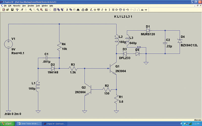
FIGURE 5. Schematic for LTspice.
This file is available at the article link. A simulation screenshot showing output voltage waveforms from the output of the secondary winding (at connection to D1) is shown in Figure 6.
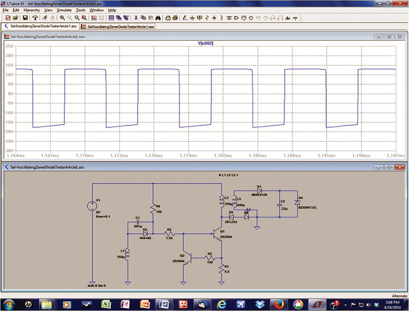
FIGURE 6. LTspice simulation — transformer output waveform.
Components in the LTspice library were used, which differed in some cases from the actual components on the schematic. The transformer is modeled as a set of coupled windings with 100% coupling (K=1 in the Spice Directive for the transformer), and all inductances are assumed to linear without any current dependency. The actual transformer used specifies a 30% inductance decline at a current of 420 mA through a single winding — well in excess of the peak current in this design — so the assumption of linearity is reasonable. Simulated circuit behavior was very close to real circuit results and was particularly useful to optimize component values.
Construction and Testing
The circuitry is constructed on a prototype printed circuit board (PCB) from RadioShack, which also is a convenient fit into a standard plastic enclosure from SeraPac with a 9V battery compartment (see Parts List). The top of the board (Figure 7) contains all the components, except the transformer, T1, which is mounted on the underside (Figure 8). T1 is configured for surface-mounting, which fits nicely on the 100 mil centers of the PCB.
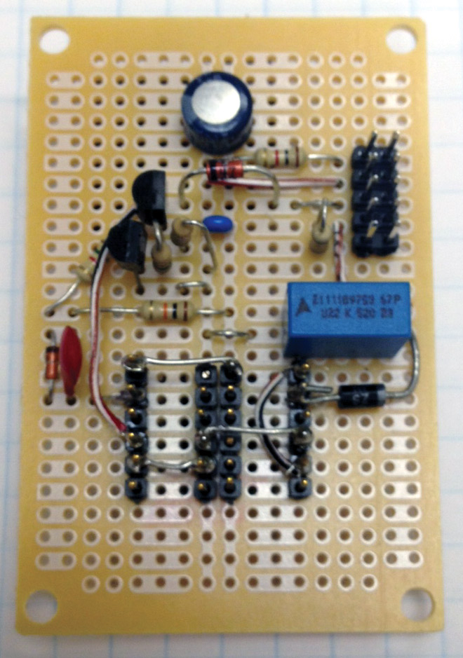
FIGURE 7. Top of assembled PCB.
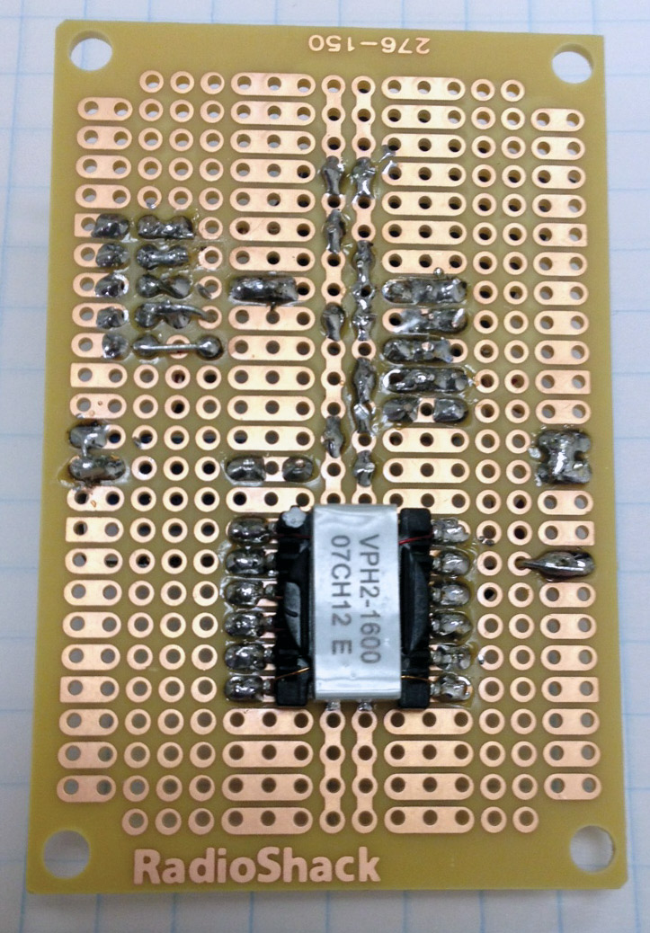
FIGURE 8. Bottom of assembled PCB.
I used pin headers for the contacts to T1 and to connect to the front panel via a flat cable (10-conductor) with a connector to the PCB (Figure 9). Neither is necessary, although I find pin headers convenient for securing oscilloscope probes when evaluating the circuit.
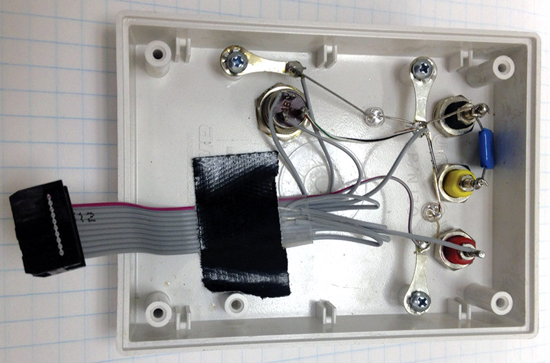
FIGURE 9. Inside of enclosure top.
Having the front panel separate and easily disconnected also facilitates board construction and modification. The only caveat in using pin headers is to make sure the switch terminals of S1 don’t contact the pin headers when the case top and bottom are put together.
All the components on the board’s topside should be mounted first and checked for continuity, and T1 soldered last on the underside. A final continuity check should be performed with the front panel connected.
Of particular importance is having D2 connected through LED2 to ground. If this connection is open, the voltage on the collector of Q1 can quickly rise to levels that will destroy the transistor.
When the continuity of the wiring checks out, connect a battery, leave the output terminals open (no DUT), and press S1. The yellow LED, LED2, should light, along with the flashing LED1. This is all you need to do to assure the circuit is operating. If the yellow LED doesn’t light, recheck your wiring.
Aside from the transformer, most of the circuit components aren’t critical but D3 must be a fast-recovery type rectifier — although any fast recovery diode with a breakdown voltage above 100 volts is acceptable. C4 and C5 should have a low equivalent series resistance (ESR) to avoid excessive ripple in the DUT. Film types are adequate in this regard, and the capacitors selected have an ESR under 0.1 ohms. If you’re not sure of the ESR of the capacitors you have, parallel several of lower value (e.g., two 0.1 µF) and make sure they have an adequate voltage rating. The low value (0.22 µF) of these capacitors is adequate for measurement accuracy, while limiting the stored energy for safety reasons.
Operating the Tester
Short the yellow to the black terminal with a jumper, connect a zener diode across the red and yellow terminals (banded side to the red terminal) along with a voltmeter, and read the voltage across the diode after pressing S1. You’ll note that as you hold S1 down, the zener voltage will drift up as the diode heats, so make a quick measurement.
Testing of LEDs and other low voltage diodes is also possible; just make sure the positive end of the LED or diode is connected to the red terminal to measure the forward voltage drop. Otherwise, the high voltage potential of the tester could destroy the LED or diode by exceeding its maximum reverse breakdown specification.
If you want to measure the current through a zener diode, remove the jumper between the yellow and black terminals and insert a millimeter. Capacitor C5 across these terminals provides a low impedance path to the pulsing current through the DUT so that the lead inductance of the multimeter doesn’t affect the readout accuracy.
When measuring an unknown zener diode and the yellow LED lights up, check to see if the diode is open by checking its forward voltage drop with a multimeter, or just reverse it in the tester. If the yellow LED goes out with the zener in the forward direction, then the diode is likely good but has a breakdown voltage above 55V. If you wish to measure the breakdown voltage in that case, insert an external variable power supply across the yellow and black terminals, with the minus terminal of the power supply connected to the yellow terminal. Increase the value of the supply slowly until the yellow LED is just extinguished, then measure the voltage across the diode.
I’ve measured zener diodes with breakdown voltages near 200V in this manner, as well as MOVs and other high voltage protective devices without concern for excessive power dissipation since the diode current when the yellow LED turns off is quite low.
Circuit Modifications and Improvements
The circuit configuration back in Figure 1 is robust and will operate with a variety of modifications. The three variable elements you can experiment with are: the secondary winding of T1; the resistor R6, which determines peak current in Q1; and the breakdown voltage of D2.
If you want the output voltage to have lower maximum voltage, you can eliminate one winding in the secondary or reduce the breakdown voltage of D2. If you want a higher maximum voltage at the output, you can put a third winding (there are two unused windings on T1) in series with the two shown, or simply replace D2 with a higher voltage zener diode. If you take this latter route, then you’ll need to pick a higher breakdown voltage transistor, like the MPSA06 (VCEO = 80V vs. 40V for the 2N3904).
Capacitors C4 and C5 are rated at 520V, and D3 has a reverse breakdown voltage of 600 volts, so there’s room to play ... but be careful if you go to higher voltages. Although C4 is a small value (0.22 µF), energy storage goes up as the square of voltage, so higher voltages can deliver a very dangerous and potentially fatal jolt! Be careful!!
If you want to increase or decrease the power delivered to the DUT, then decrease or increase the value of R6, respectively. Both 2N4401 and MPSA06 transistors can support peak currents up to 500 mA and are usable in this circuit.
It would also be easy to use a larger enclosure for the tester and include a digital panel meter that would read out the zener diode voltage without requiring a separate meter, or two to read voltage and current simultaneously.
There you have it! I hope this circuit measures up for you as much as it has for me! NV
References
Switchmode Power Supply Handbook, Keith Billings, McGraw-Hill, 1989, pp. 2.49 to 2.62.
VERSA-PAC Transformer Information: www.digikey.com/product-search/en?mpart=VPH2-1600-R&vendor=283
EDN Magazine, June 10, 2010, Design Ideas, pp. 51-52, “Circuit lets you measure zener voltages and test LEDs.”
EDN Magazine, November 25, 2004, pp. 104-106, “Zener test circuit serves as a DC source.”
Corrections
Part list updated. Download zip file for updated Parts List.
Downloads
November2014_Hoffman-Parts