Previously, I detailed the assembly of a headset amplifier. This time, we'll discuss the theory of operation behind that amplifier. However, most of this discussion will apply to the power amplifier described in the August issue, as well.
PERFORMANCE
Despite the fact my headset project used inexpensive parts, the resulting amplifier (a diagram of which is shown in Figure 1) is a high quality device with very low distortion and noise, and a flat frequency response over the audio frequency range and well beyond.
Distortion is also excellent — less than 0.0012% from 20 Hz to 1 kHz, increasing to 0.0021% at 20 kHz as measured with my HP 339A with a 1K load. With a 100 ohm load, distortion increases somewhat to 0.0016% at low frequencies and 0.008% at 20 kHz. At 10 kHz with this load, it measures about 0.005%. The level at 1K load is right at the limit of the sensitivity of this instrument.
Distortion is probably considerably lower than this. Traditional distortion analyzers measure distortion plus noise. THD+N is the common nomenclature: Total Harmonic Distortion plus Noise. Essentially, these instruments tune out the fundamental frequency signal and measure everything else, which includes noise and harmonics. The breadboard circuit produces no audible noise in the headset with no input signal. Measured noise at the amplifier output with a 1K load and a measurement bandwidth of 100 kHz is 20 microvolts.
How good is good enough?
It is commonly accepted that 0.1% harmonic distortion is about the limit of audibility. A worse problem is that harmonic distortion indicates non-linearity of the circuit which can produce what is called intermodulation distortion. Low harmonic distortion guarantees low intermodulation distortion. I've tested myself by listening to a pure 500 Hz tone and then gradually injecting a second harmonic until I could just hear it. The distortion analyzer indicated 0.08% harmonic at that point. I feel that it would take considerably more than that to be heard when listening to music.
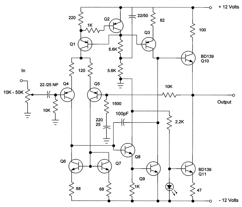
FIGURE 1. Schematic Diagram
| Transistors |
| Q1-5 2N5401 PNP |
| Q6-9 2N5551 NPN |
| Q10-11 BD139 |
| Resistors - All 1/4 watt 5% carbon film |
| Electrolytic capacitor voltages as marked. The 100 pF capacitor must be mica or NPO ceramic. |
DESIGN
How can such an inexpensive circuit have such impressive performance? The short answer is that the design is much more important than the cost of the components. I take no credit for the design except for the output stage with its inherent shortcircuit protection. The rest of the project is an implementation of an inexpensive amplifier and the verification of its performance.
Since the 1960s, there has been one dominant arrangement or architecture used for most power amplifiers. This design approach was developed by Dr. Hung C. Lin who worked for RCA in the early days of transistors in the area of developing applications. (Google "Dr. Lin RCA" to find interesting articles about him). This has come to be known as the Lin architecture.
There are many variations on this basic design. We have started with (almost) the simplest of them. Because this project incorporates the first two stages of most modern solid-state power amplifiers, the same design can be used to build a low to medium power audio amplifier.
Transistors are not inherently linear devices. Much can be done to make them linear and minimize distortion. A good start for an input stage is to use a pair of transistors in differential mode (Q4 and Q5). A differential input stage reduces the second harmonic to a very low level if it is balanced accurately. The differential stage has two inputs. This provides a very convenient way to connect negative feedback to establish the gain of the amplifier and to reduce distortion.
The pair of transistors in this stage work in opposition to each other. If the signal current goes up in one, it goes down by the same amount in the other. The non-linearities in the two cancel each other. The extent of the cancellation depends on the balance of the two. The 120 ohm emitter resistors reduce the gain of the stage somewhat and also reduce the distortion. They make the matching of the two transistors less critical.
Transistors Q1-Q3 at the top of the diagram comprise a voltage reference and two current sources. Q2 is the reference. It controls the emitter voltage on Q1 and Q3. The current is adjusted by the value of the emitter resistor in the current source transistor. The input differential amplifier's current source is about 3 mA, set by the 220 ohm emitter resistor on Q1.
Using a current source provides a reduction in distortion when compared to using a resistor. It also greatly improves the "power supply rejection" — the sensitivity to power supply ripple. For pennies, the improvement in the circuit it provides makes it very much worth including.
The voltage reference is such that about 0.64 volts appear across the 220 ohm resistor — a current of about 3 mA. This source provides what is commonly called the "tail current" and the input stage is called a "long tailed pair." An ideal current source would provide absolutely constant current regardless of the load resistance over a wide range. This simple circuit comes close.
Balance is critical so the load for the differential stage is a "current mirror" (Q6 and Q7). It provides an active load for the transistor and it balances the current between the two transistors at zero signal, so the current is very nearly the same in each. The current mirror has emitter resistors of 68 ohms which compensate for small differences in Vbe and beta. The addition of these two inexpensive transistors and a pair of resistors can improve the distortion level by a factor of 100.
Incidentally, I've built a number of amplifiers using this input stage configuration and have never matched the transistor pairs. The circuit is more or less immune to variations in transistor beta and Vbe.
This first stage drives the base of Q8 which has its emitter connected to the base of Q9. This arrangement greatly enhances the current gain of this second stage. The first stage is a "transconductance" stage which simply means that it converts the input voltage to a current. The second stage converts that current to a signal voltage. We want a large voltage gain in this stage, so we use a current source as the load.
This source is about 8 mA provided by Q3. It uses the same reference voltage as the first stage's current source. The 82 ohm emitter resistor sets the current. The AC impedance of the current source is greater than half a megohm, which makes the voltage gain high. This second stage is called the voltage amplifier stage, or VAS for short.
In this simple amplifier, the output of the VAS drives an emitter follower output device. Q11 is a current source which acts as a load for the emitter follower Q10. (Yes, I know by convention this is a current sink.) The green LED acts as a voltage reference of about 2.1 volts. The 2.2K ohm resistor supplies about 5 mA to turn it on. The reference voltage is applied to the base of the current source transistor. The emitter resistor of the current source is 47 ohms, which sets the current at about 35 mA. The exact value is not critical.
The current from the positive supply through Q10 is limited by the 100 ohm resistor in the collector. The power dissipation in the output transistors is about 0.35 watts in each with no signal. The output transistors could operate without the heatsinks and be well within their ratings, but I like to play it safe. This is a Class A output stage.
The current source active load is better than a resistor because it can supply full current to the output even when the signal voltage nears the negative supply voltage. The 100 ohm resistor in series with the positive supply protects the amplifier output from accidental shortcircuits of a short duration, i.e., a second or two. In the case of a long term short, this resistor will become a fuse!
In order to keep the circuit from becoming an oscillator, there is a compensating capacitor from the collector of the VAS to the base of the input follower transistor. Ordinary ceramic capacitors are notorious for changing value as the applied voltage changes. If you use a ceramic here, it must be of the NPO type (indicating that the voltage coefficient of capacitance is around zero, but may be slightly negative or positive). A mica capacitor is a little more expensive but guaranteed to work well.
The various transistors in the signal path each have an upper frequency limit. That is, they act like a low pass filter. Each additional transistor in the signal path contributes phase shift at some high frequency. This phase shift is cumulative and if it reaches the point where the negative feedback becomes positive, the result will be a peak in the high frequency response. A little more phase shift produces an oscillator at some high frequency.
The purpose of the compensating capacitor is to provide a low pass filter much lower than any of the others, so that the frequency response is reduced as frequency increases. As long as the "open loop" gain of the amplifier reaches unity as frequency increases before the phase shift exceeds 90 degrees by "too much," the amplifier will be stable when negative feedback is applied. "Too much" is rather ambiguous. That is a long story beyond the scope of this article. (If you are interested in pursuing this topic, look up "phase margin" in any of the books listed in the sidebar.)
Notice that a 10K resistor is connected to the output that goes back to the negative input of the first stage. This is the negative feedback path. This resistor and the 1,500 ohm resistor to the 220 µF capacitor form a voltage divider that sets the amount of negative feedback, and thus the AC gain of the amplifier — about 7.7. The 220 µF capacitor allows full DC voltage feedback, so the output DC voltage can be on the order of a few millivolts.
(The voltage on the 220 µF capacitor will be positive a few tenths of a volt in normal operation, so it need not be the non-polar type). The amplifier's voltage gain at DC is unity. Note that the signal gain of the amplifier without feedback is VERY high. The amplifier won't work without the feedback connected because it is the feedback that puts the operating point of the voltage amplifier stage such that the output is near zero with no signal. (Whew!)
What we have built here is a discrete component operational amplifier capable of a little more power output than most of the integrated circuit ones.
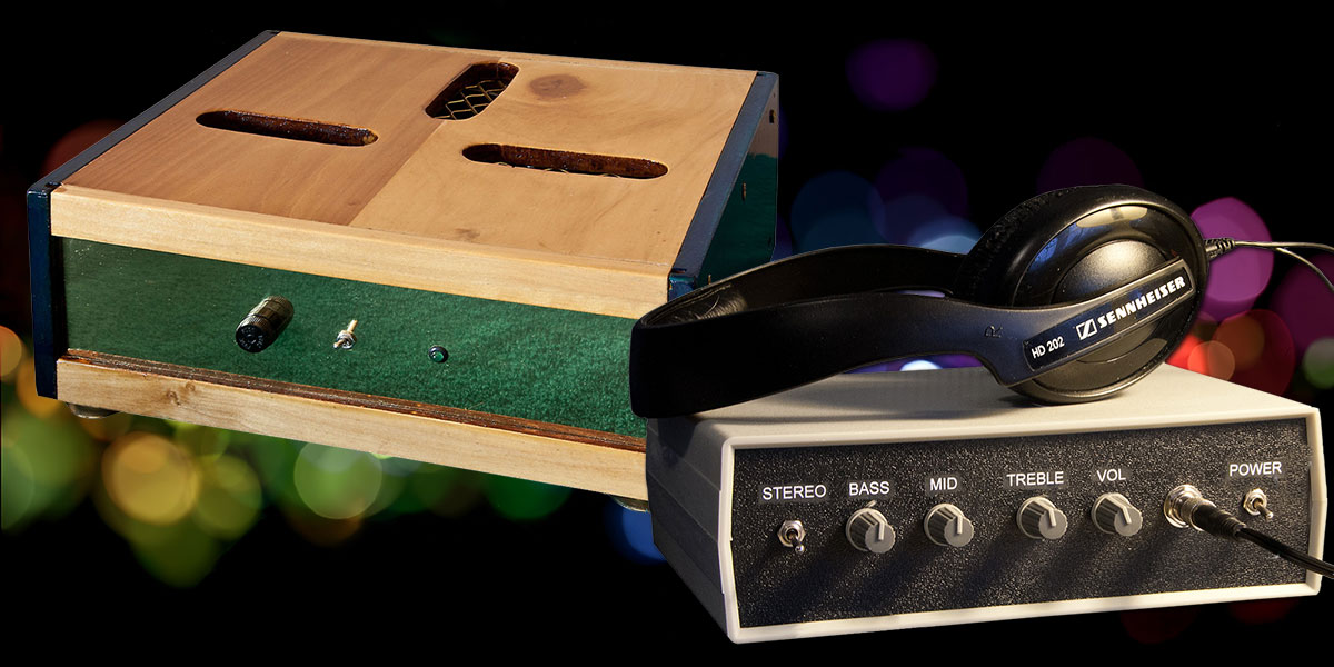
HEADSETS
Headset impedance varies from 600 ohms down to 24 ohms — possibly beyond this range. The volume control at the input will allow almost any signal source to drive the amplifier to overload, so turn it up from zero until the headset signal is sufficiently loud.
An amplifier on perfboard laying on a bench is an accident waiting to happen. Mount your board in a project box on some standoffs. Of course, you will want the box to be large enough for two channels. Place the power transformer as far from the input connections as you can.
I've tested this amplifier with the following headphones: a Sennheiser HD 202 (32 ohms, approx. $30); a Sennheiser HD 650 (330 ohms, $400-$500); and with a AKG 702 (60 ohms, $350-$539). The AKG seems the least sensitive. I prefer the HD 202 to the AKG. The HD 650 is great!
DAMPING
Audio folks discuss the damping factor as important to a loudspeaker. Damping factor is the ratio of the speaker or headset impedance to the amplifier output impedance.
References online indicate that for a headset, a damping factor of eight or more is adequate. This amplifier's output impedance is less than 0.05 ohms, so the damping factors are quite high.
I've measured the impedance vs. frequency of the three headsets I just listed. All have a slight peak at about 50 Hz. One set measured about 15% higher impedance at the peak, and a better one was about 10%. A low damping factor would result in the bass response being up about 1.5 dB at 50 Hz in one case, and 1 dB in the other.
This is a small difference but probably detectable by someone with good ears. That is, with a low damping factor this might be audible.
A high damping factor greatly reduces the peak in the response.
In this design, I agonized over damping factor vs. protection of the amplifier and headset. Initially, I had the 100 ohm resistor in series with the output which provides current limiting, but a terrible damping factor for low impedance headsets. Putting the resistor in the collector circuit of the output follower gives the same current-limiting protection but the negative feedback from the output decreases the output impedance (as long as the amplifier is not overloaded) to a fraction of an ohm. Hopefully, this discussion will help when you design your own projects. NV
REFERENCES
High-Power Audio Amplifier Construction Manual
by G. Randy Slone, McGraw Hill 1999
This one is useful as a project book. Many of the designs are suitable for building. It is much more than a construction manual, however. Slone discusses the most prevalent designs in audio amplifiers. Not a great deal has changed in the years since the writing of this book, though some of the transistors used in these designs are either hard to find or expensive due to their scarcity. They are still available if you look hard enough. Slone discusses subjectivity briefly.
The Audiophile's Project Sourcebook
by G. Randy Slone. TAB division of McGraw Hill 2002
This book has a number of audio projects of various complexity including stepped attenuators, various preamplifiers and tone control circuits, electronic crossover networks, power amplifiers, an electronic reverberation circuit, and many more. This one is a cookbook.
Audio Power Amplifier Design Handbook
by Doug Self, Focal Press 5th Edition 2009
This is the most technical of the books, containing lots of data interesting to an engineer. It covers a number of design possibilities. Self enumerates the causes of distortion in an amplifier and systematically shows how to minimize each of them, resulting in what he calls the "blameless" amplifier. It is not "perfect," but all the known sources of distortion have been considered and adjusted to minimize the distortion. This book has the best discussion of subjectivity. An older version (i.e., the fourth edition) may still be available. There is a LOT of new material in the fifth edition.
Designing Audio Power Amplifiers
by Bob Cordell, McGraw Hill 2011
Bob has the ability to describe much of the technical detail in a way that is more intuitive than most authors. It is not a cookbook, but it is a good discussion of the subject. The circuits in this book use transistors that are newer and more available (and less expensive and a bit less capable) than those in Slone's book.
All of the above books discuss the (now almost) standard three-stage Lin architecture and numerous variations for each stage. Self describes some of these improvements in detail and concludes that though the "numbers" are better, the improvement is not audible. Perfection is a worthy goal, however, never to be achieved in an audio power amplifier, but some designs come very close. I purchased all four of these books at Amazon.com. I'm not sure all are still available there.
What is subjectivity and the subjectivist movement? Follow this link for some interesting reading. You don't have to understand all of it to appreciate what Doug Self has to say at www.douglas-self.com/ampins/pseudo/subjectv.htm. The discussion is almost word for word from a section of his book mentioned above.