Our opening episode of this four-part ‘op-amp’ series described the basic operating principles of conventional voltage-differencing op-amps (typified by the 741 type) and showed some basic circuit configurations in which they can be used. This installment looks at practical ways of using such op-amps in linear amplifier and active filter applications.
When reading this episode, note that all practical circuits are shown designed around a standard 741-type op-amp and operated from dual 9V supplies, but that these circuits will usually work (without modification) with most voltage-differencing op-amps, and from any DC supply within that op-amp’s operating range (allowing for possible differences in the op-amp’s offset biasing networks).
INVERTING AMPLIFIER CIRCUITS
Figure 1 shows the practical circuit of an inverting DC amplifier with an overall voltage gain (A) of x10 (= 20dB), and with an offset nulling facility that enables the output to be set to precisely zero with zero applied input. The voltage gain and input impedance are determined by the R1 and R2 values, and can be altered to suit individual needs. The gain can be made variable — if required — by using a series combination of a fixed and a variable resistor in place of R2. For optimum biasing stability, R3 should have a value equal to the parallel values of R1 and R2.
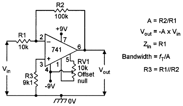 |
| FIGURE 1. Inverting DC amplifier with offset-nulling facility and x10 voltage gain. |
Note that the Figure 1 circuit will continue to function if the RV1 offset-nulling network is removed, but its output may offset by an amount equal to the op-amp’s input offset voltage (typically 1mV in a 741) multiplied by the closed-loop voltage gain (A) of the circuit, e.g., if the circuit has a gain of x100, the output may be offset by 100mV with zero input applied.
Also note that the circuit’s bandwidth equals the fT value (typically 1MHz in a 741) divided by the ‘A’ value, e.g., the Figure 1 circuit gives a bandwidth of 100kHz with a gain of x10, or 10kHz with a gain of x100.
 |
| FIGURE 2. Inverting AC amplifier with x10 gain. |
The Figure 1 circuit can be adapted for use as an AC amplifier by simply wiring a blocking capacitor in series with the input terminal, as shown in Figure 2. Note in this case that no offset nulling facility is needed, and that (for optimum biasing) R3 is given a value equal to R2.
NON-INVERTING AMPLIFIER CIRCUITS
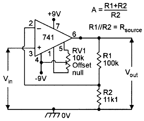
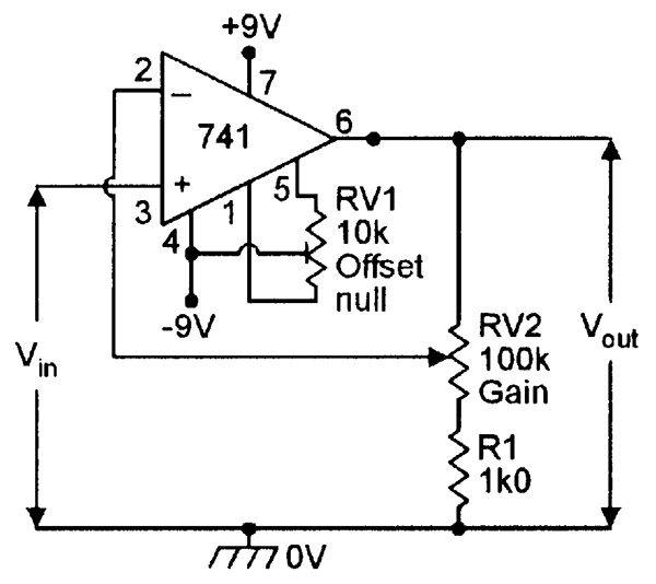
An op-amp can be used as a non-inverting DC amplifier with offset compensation by using the connections shown in Figure 3, which shows an x10 amplifier. The voltage gain is determined by the ratios of R1 and R2, as indicated. If R1 is given a value of zero, the gain falls to unity; alternatively, if R2 is given a value of zero, the gain equals the open-loop gain of the op-amp. The gain can thus be made variable by replacing R1 with a pot and connecting its slider to the inverting terminal of the op-amp, as shown in the circuit in Figure 4, in which the gain can be varied over the range x1 to x101 via RV2.
 |
 |
| FIGURE 3. Non-inverting DC amplifier with offset-nulling facility and x10 gain. |
FIGURE 4. Non-inverting variable gain (x1 to x101) DC amplifier. |
Note that — for correct operation — the input (non-inverting) terminal of each of these circuits must be provided with a DC path to the common or zero-volts rail; this path is provided by the DC input signal. In Figure 3, the parallel values of R1 and R2 should ideally (for optimum biasing) have a value equal to the source resistance of the input signal.
A major feature of the non-inverting op-amp circuit is that it gives a very high input impedance. In theory, this impedance is equal to the open-loop input resistance (typically 1M0 in a bipolar 741) multiplied by AO/A. In practice, input impedance values of hundreds of megohms can easily be obtained in DC circuits such as those in Figures 3 and 4.
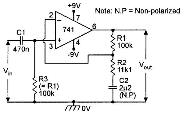
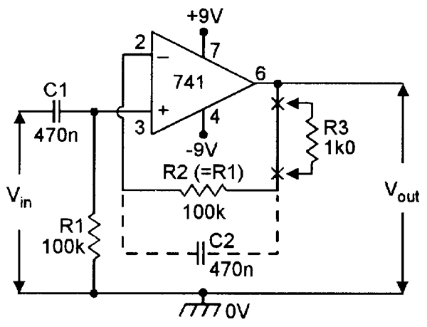
Figure 5 shows how the Figure 3 circuit can be modified for use as an x10 non-inverting AC amplifier by removing the offset biasing network, connecting the non-inverting terminal to ground via biasing resistor R3, and connecting the input signal via a blocking capacitor. Note that gain-control resistors R1-R2 are isolated from ground via blocking capacitor C2, which has negligible impedance at practical operating frequencies; the voltage gain is thus determined by the ratios of R1 and R2, but the op-amp’s inverting terminal is subjected to virtually 100% DC negative feedback, thus giving the circuit excellent DC stability. For optimum biasing, R3 should have the same value as R1.
 |
 |
| FIGURE 5. Non-inverting x10 AC amplifier with 100k input impedance. |
FIGURE 6. Non-inverting x10 AC amplifier with 50M input impedance. |
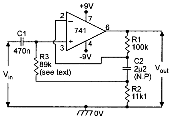
Note that the input impedance of the Figure 5 circuit equals the R3 value, and is limited to a few megohms by practical considerations. Figure 6 shows how the basic circuit can be modified to give a very high input impedance (typically 50 megohms).
Here, the positions of C2 and R2 are transposed, and the low end of R3 is tied to the C2-R2 junction. As a consequence, near-identical operating (AC) signal voltages appear at both ends of R3, which thus passes negligible signal current and has an apparent impedance that is massively increased by this ‘bootstrap’ action.
In practice, the circuit’s input impedance is typically limited to about 50 megohms by leakage impedances of the op-amp’s socket and the PCB to which it is wired. Note that — for optimum DC biasing — the sum of the R2 and R3 values should equal R1. In practice, the R3 value can differ from this ideal by up to 30%, and an actual value of 100k can be used in the Figure 6 circui, if desired.
VOLTAGE FOLLOWER CIRCUITS
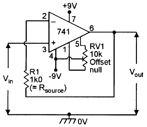
A voltage follower circuit produces an output voltage that is identical to that of the input signal, but has a very high input impedance and a very low output impedance. The circuit actually functions as a unity-gain non-inverting amplifier with 100% negative feedback. Figure 7 shows the idealized design of a precision voltage follower with offset biasing. Note that — for optimum biasing — feedback resistor R1 should have a value equal to the source resistance of the input signal.
In practice, the basic Figure 7 circuit can often be greatly simplified. Eliminating the offset biasing network, for example, adds an error of only a few mV to the output of the op-amp. Again, the value of feedback resistor R1 can be varied from zero to 100k without greatly influencing the circuit’s accuracy.
 |
 |
| FIGURE 7. Precision DC voltage follower with offset null facility. |
FIGURE 8. AC voltage follower with 100k input impedance. |
If an op-amp with a low fT value (such as the 741) is used, the R1 value can usually be reduced to zero. Note, however, that many ‘high fT’ op-amps tend towards instability when used in the unity-gain mode and, in such cases, R1 should be given a value of 1k0 or greater to effectively reduce the circuit’s bandwidth and thus enhance stability.
Figure 8 shows an AC version of the voltage follower. In this case, the input signal is DC-blocked via C1, and the op-amp’s non-inverting terminal is tied to ground via R1, which determined the circuit’s input impedance. Ideally, feedback resistor R2 should have the same value as R1. If R2 has a high value, however, it may significantly reduce the circuit’s bandwidth. This problem can be overcome by shunting R2 with C2, as shown dotted. If the latter technique is used with a ‘high fT’ op-amp, resistor R3 can be connected as shown to ensure circuit stability.
If a very high input impedance is required from an AC voltage follower, it can be obtained by using the basic configuration shown in Figure 9, in which R1 is ‘bootstrapped’ from the op-amp output via C2, thus raising its impedance to near-infinity. In practice, this circuit can easily give an input impedance of 50 megohms from a 741 op-amp; this limit being set by the leakage impedance of the op-amp’s IC socket and the PCB.
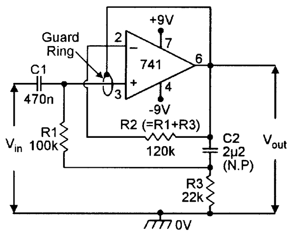 |
| FIGURE 9. AC voltage follower with 50M input impedance without the guard ring, or 500M with the guard ring. |
If an even greater input impedance is needed, the area of PCB surrounding the op-amp input pin should be provided with a printed ‘guard ring’ that is driven from the op-amp output, as shown, so that the leakage impedances of the PCB, etc., are themselves bootstrapped and raised to near-infinite values. In this case, the Figure 9 circuit gives an input impedance of about 500 megohms when used with a 741 op-amp, or even greater if an FET-input op-amp is used.
CURRENT-BOOSTED ‘FOLLOWER’ CIRCUITS
Most op-amps can provide maximum output currents of only a few milliamps, and this is the current-driving limit of the voltage follower circuits in Figures 7 to 9. The current-driving capacity of a voltage follower can easily be increased, however, by wiring a simple or a complementary emitter follower current booster stage between the op-amp output and the final output terminal of the circuit, as shown in the basic designs in Figures 10 and 11. Note that the base-emitter junctions of the transistors are wired into the negative feedback loop of the op-amp, to minimize the effects of junction non-linearity.
 |
 |
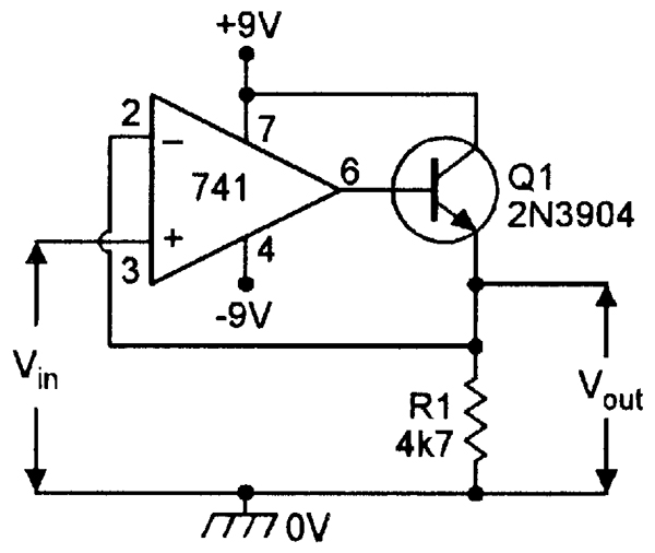
| FIGURE 10. Unidirectional DC voltage follower with boosted output-current drive. |
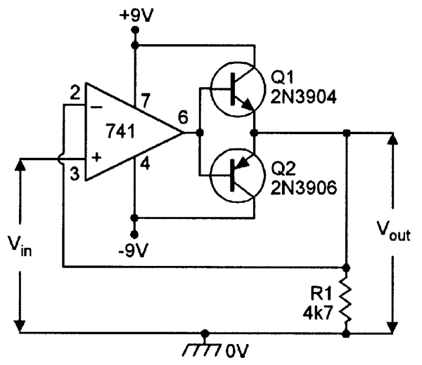
FIGURE 11. Bidirectional DC voltage follower with boosted output-current drive. |
The Figure 10 circuit is able to source large currents (via Q1), but can sink only relatively small ones (via R1). This circuit can thus be regarded as a unidirectional, positive-only, DC voltage follower.
The Figure 11 circuit can both source (via Q1) and sink (via Q2) large output currents, and can be regarded as a bidirectional (positive and negative) voltage follower. In the simple form shown in the diagram, the circuit produces significant cross-over distortion as the output moves around the zero volts value. This distortion can be eliminated by suitably biasing Q1 and Q2.
In practice, the Figure 10 and 11 circuits have maximum current-drive capacities of about 50mA, this figure being dictated by the low power ratings of the specified transistors. Greater drive capacity can be obtained by using alternative transistors.
ADDERS AND SUBTRACTORS
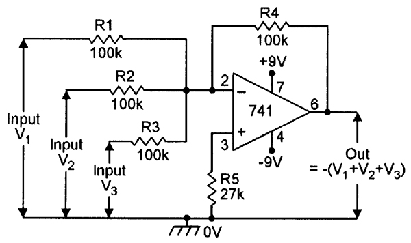
Figure 12 shows the circuit of a unity-gain analog DC voltage adder, which gives an inverted output voltage equal to the sum of the three input voltages. Input resistors R1 to R3 and feedback resistor R4 have identical values, so the circuit acts as a unity-gain inverting DC amplifier between each input terminal and the output. The current flowing in R4 is equal to the sum of the R1 to R3 currents, and the inverted output voltage is thus equal to the sum of the input voltages. In high-precision applications, the circuit can be provided with an offset nulling facility.
 |
 |
| FIGURE 12. Unity-gain inverting DC adder. |
FIGURE 13. Unity-gain audio mixer. |
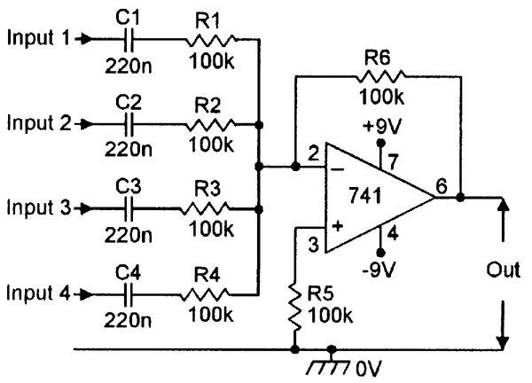
The Figure 12 circuit is shown with three input connections, but can, in fact, be given any number of inputs (each with a value equal to R1), but in this case, the R5 value should (for optimum biasing) be altered to equal the parallel values of all other resistors. If required, the circuit can be made to give a voltage gain greater than unity by simply increasing the value of feedback resistor R4. The circuit can be used as a multi-input ‘audio mixer’ by AC-coupling the input signals and giving R5 the same value as the feedback resistor, as shown in the four-input circuit in Figure 13.
 |
| FIGURE 14. Unity-gain DC differential amplifier, or subtractor. |
Figure 14 shows the circuit of a unity-gain DC differential amplifier, or analog subtractor, in which the output equals the difference between the two input signal voltages, i.e., equals e2 - e1. In this type of circuit, the component values are chosen such that R1/R2 = R3/R4, in which case, the voltage gain, A, equals R2/R1. When — in Figure 14 — R1 and R2 have equal values, the circuit gives unity overall gain, and thus acts as an analog subtractor.
BALANCED PHASE-SPLITTER
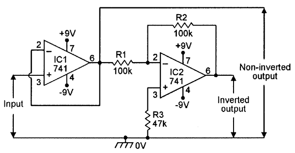
A phase-splitter has a pair of output terminals, which produce outputs that are identical in amplitude and form, but with one output phase-shifted by 180° (i.e., inverted) relative to the other. Figure 15 shows an easy way of making a unity-gain balanced DC phase-splitter, using a pair of 741 op-amps.
 |
| FIGURE 15. Unity-gain balanced DC phase-splitter. |
Here, IC1 acts as a unity-gain non-inverting amplifier or voltage follower, and provides a buffered output signal that is identical to that of the input.
This output also provides the input drive to IC2, which acts as a unity-gain inverting amplifier, and provides the second output, which is inverted but is otherwise identical to the original input signal.
ACTIVE FILTERS
Filter circuits are used to reject unwanted frequencies and pass only those wanted by the designer. A simple R-C low-pass filter (Figure 16(a)) passes low-frequency signals, but rejects high-frequency ones.
The output falls by 3dB at a ‘break’ or ‘cross-over’ frequency (fC) of 1/2πRC), and then falls at a rate of 6dB/octave (= 20dB/decade) as the frequency is increased (see Figure 16(b)). Thus, a simple 1kHz filter gives roughly 12dB of rejection to a 4kHz signal, and 20dB to a 10kHz one.
 |
| FIGURE 16. Circuit and response curves of simple 1st-order R-C filters. |
A simple R-C high-pass filter (Figure 16(c)) passes high-frequency signals, but rejects low-frequency ones. The output is 3dB down at a break frequency of 1/2πRC), and then falls at a 6dB/octave rate as the frequency is decreased below this value (Figure 16(d)). Thus, a simple 1kHz filter gives roughly 12dB of rejection to a 250Hz signal, or 20dB to a 100Hz signal.
Each of the above two filter circuits uses a single R-C stage, and is known as a ‘1st order’ filter. If a number (n) of similar filters are effectively cascaded, the resulting circuit is known as an ‘nth order’ filter and has an output slope, beyond fC, of (n x 6dB)/octave.
Thus, a 4th order 1kHz low-pass filter has a slope of 24dB/octave, and gives 48dB of rejection to a 4kHz signal, and 80dB to a 10kHz signal.
One way of effectively cascading such filters is to wire them into the feedback networks of suitable op-amp amplifiers; such circuits are known as ‘active filters,’ and Figures 17 to 23 show practical examples of some of them.
ACTIVE FILTER CIRCUITS
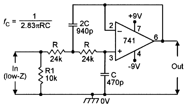
Figure 17 shows the practical circuit and formula of a maximally-flat (Butterworth) unity-gain 2nd-order low-pass filter with a 10kHz break frequency. Its output falls off at a 12dB/octave rate beyond 10kHz, and is about 40dB down at 100kHz, and so on. To change the break frequency, simply change either the R or the C value in proportion to the frequency ratio relative to Figure 17; reduce the values by this ratio to increase the frequency, or increase them to reduce it. Thus, for 4kHz operation, increase the R values by a ratio of 10kHz/4kHz, or 2.5 times.
 |
 |
| FIGURE 17. Unity-gain 2nd-order 10kHz low-pass active filter. |
FIGURE 18. ‘Equal components’ version of 2nd-order 10kHz low-pass active filter. |
A minor snag with the Figure 17 circuit is that one of its C values must be twice the value of the other, and this may demand odd component values. Figure 18 shows an alternative 2nd-order 10kHz low-pass filter circuit that overcomes this snag and uses equal component values. Note here that the op-amp is designed to give a voltage gain (4.1dB in this case) via R1 and R2, which must have the values shown.
 |
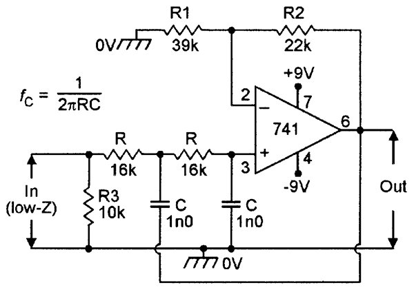
| FIGURE 19. 4th-order 10kHz low-pass filter. |
Figure 19 shows how two of these ‘equal component’ filters can be cascaded to make a 4th-order low-pass filter with a slope of 24dB/octave. Note in this case that gain-determining resistors R1/R2 have a ratio of 6.644, and R3/R4 have a ratio of 0.805, giving an overall voltage gain of 8.3dB. The odd values of R2 and R4 can be made up by series-connecting 5% resistors.
 |
 |
| FIGURE 20. Unity-gain 2nd-order 100Hz high-pass filter. |
FIGURE 21. ‘Equal components’ version of 2nd-order 100Hz high-pass filter. |
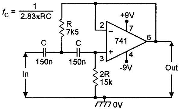
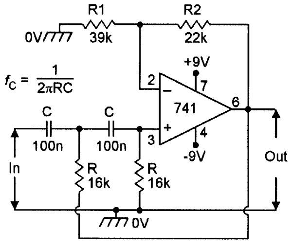
Figures 20 and 21 show unity-gain and ‘equal component’ versions respectively of 2nd-order 100Hz high-pass filters, and Figure 22 shows a 4th-order 100Hz high-pass filter. The operating frequencies of these circuits, and those of Figures 18 and 19, can be altered in exactly the same way as in Figure 17, i.e., by increasing the R or C values to reduce the break frequency, or vice versa.
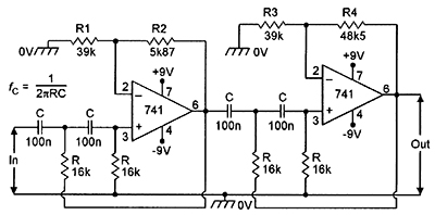 |
| FIGURE 22. 4th-order 100Hz high-pass filter. |
Finally, to complete this installment of the series, Figure 23 shows how the Figure 21 high-pass and Figure 18 low-pass filters can be wired in series to make (with suitable component value changes) a 300Hz to 3.4kHz speech filter that gives 12dB/octave rejection to all signals outside of this range.
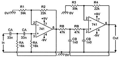 |
| FIGURE 23. 300Hz to 3.4kHz speech filter with 2nd-order response. |
In the case of the high-pass filter, the C values in Figure 21 are reduced by a factor of three, to raise the break frequency from 100Hz to 300Hz and, in the case of the low-pass filter, the R values in Figure 18 are increased by a factor of 2.94, to reduce the break frequency from 10kHz to 3.4kHz. NV
Next time, we'll look at practical op-amp oscillators and switching circuits in the third installment of this four-part series.