The opening episode of this ‘op-amp’ series described the basic operating principles of conventional voltage-differencing op-amps (typified by the 741 type), and showed some basic circuit configurations in which they can be used. The present episode looks at practical ways of using such op-amps in various oscillator and switching applications.
When reading this installment, note that most practical circuits are shown designed around a standard 741 or 3140-type op-amp and operated from dual 9V supplies, but that these circuits will usually work (without modification) with most voltage-differencing op-amps, and from any DC supply within that op-amp’s operating range.
SINEWAVE OSCILLATORS
An op-amp can be made to act as a sinewave oscillator by connecting it as a linear amplifier in the basic configuration shown in Figure 1, in which the amplifier output is fed back to the input via a frequency-selective network, and the overall gain of the amplifier is controlled via a level-sensing system.
 |
| Figure 1. Conditions for stable sinewave oscillation. |
For optimum sinewave generation, the feedback network must provide an overall phase shift of zero degrees and a gain of unity at the desired frequency. If the overall gain is less than unity, the circuit will not oscillate and, if it is greater than unity, the output waveform will be distorted.
 |
| Figure 2. Basic Wien Bridge sinewave oscillator. |
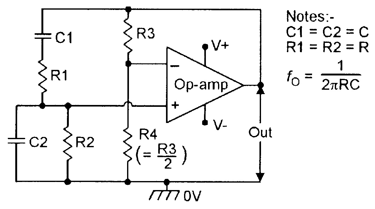
One way of implementing the above principle is to connect a Wien Bridge network and an op-amp in the basic configuration shown in Figure 2. Here, the frequency-sensitive Wien Bridge network is constructed from R1-C1 and R2-C2. Normally, the network is symmetrical, so that C1 = C2 = C, and R1 = R2 = R. The main feature of the Wien network is that the phase relationship of its output-to-input signals varies from -90° to +90°, and is precisely 0° at a center frequency (fO) of 1/2πpCR. At this center frequency, the symmetrical network has a voltage gain of 0.33.
Thus, in Figure 2, the Wien network is connected between the output and the non-inverting input of the op-amp, so that the circuit gives zero overall phase shift at fO, and the actual amplifier is given a voltage gain of x3 via feedback network R3-R4, to give the total system an overall gain of unity.
The circuit thus provides the basic requirements of sinewave oscillation. In practice, however, the ratios of R3-R4 must be carefully adjusted to give overall voltage gain of precise unity that is necessary for low-distortion sinewave generation.
The basic Figure 2 circuit can easily be modified to give automatic gain adjustment and amplitude stability by replacing the passive R3-R4 gain-determining network with an active gain-control network that is sensitive to the amplitude of the output signal, so that gain decreases as the mean output amplitude increases, and vice versa. Figures 3 to 7 show some practical versions of Wien Bridge oscillators with automatic amplitude stabilization.
THERMISTOR-STABILIZED CIRCUITS
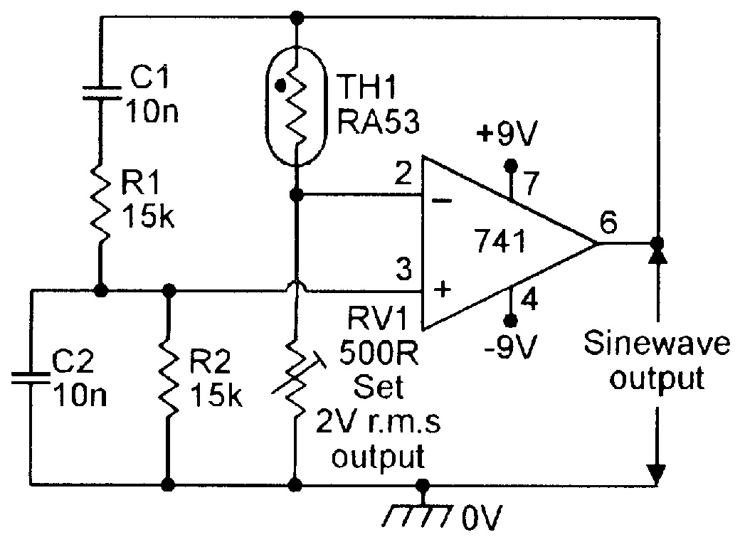
Figure 3 shows the basic circuit of a 1kHz thermistor-stabilized Wien bridge oscillator of the type that has been popular in the UK and other European countries for many years. The thermistor used here is a rather expensive and delicate RA53 (or similar) negative-temperature-coefficient (ntc) type. The thermistor (TH1) and RV1 form a gain-determining network.
 |
| Figure 3. Thermistor stabilized 1kHz Wien Bridge oscillator. |
The thermistor is heated by the mean output power of the op-amp, and at the desired output signal level has a resistance value double that of RV1, thus giving the op-amp a gain of x3 and the overall circuit a gain of unity. If the oscillator output starts to rise, TH1 heats up and reduces its resistance, thereby automatically reducing the circuit’s gain and stabilizing the amplitude of the output signal.
 |
| Figure 4. 150Hz-1.5kHz lamp-stabilized Wien Bridge oscillator. |
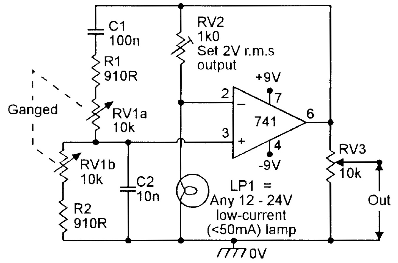
An alternative method of thermistor stabilization is shown in Figure 4; this circuit variant is very popular in the USA. In this circuit, a low-current filament lamp is used as a positive-temperature-coefficient (ptc) thermistor, and is placed in the lower part of the gain-determining feedback network.
Thus, if the output amplitude increases, the lamp heats up and increases its resistance, thereby reducing the circuit gain and providing automatic amplitude stabilization. This circuit also shows how the Wien network can be modified by using a twin-gang pot to make the oscillator frequency variable over the range 150Hz to 1.5kHz, and how the sinewave output amplitude can be made variable via RV3.
Note in the Figure 3 and 4 circuits that the pre-set pot should be adjusted to set the maximum mean output signal level to about 2V RMS, and that under this condition, the sinewave has a typical total harmonic distortion (THD) level of about 0.1%.
If the circuit’s thermistor is a low-resistance type, it may be necessary to interpose a bidirectional current-booster stage between the op-amp output and the input of the amplitude control network, to give it adequate drive.
Finally, a slightly annoying feature of thermistor-stabilized circuits is that, in variable-frequency applications, the sinewave’s output amplitude tends to judder or ‘bounce’ as the frequency control pot is swept up and down its range.
DIODE-STABILIZATION CIRCUITS
 |
| Figure 5. Diode-regulated 150Hz-1.5kHz Wien Bridge oscillator. |
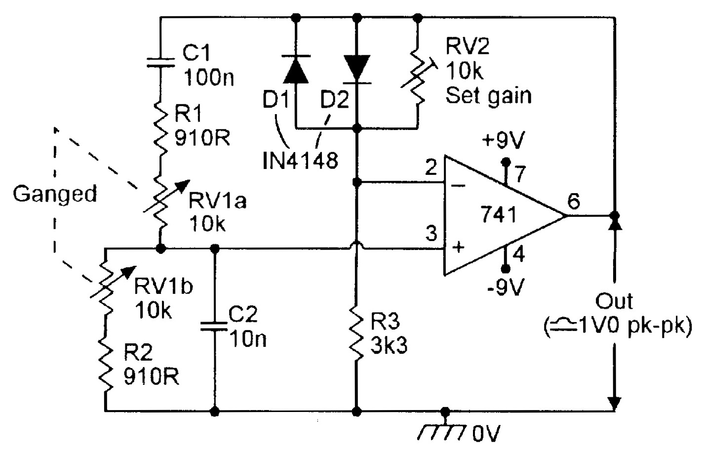
The amplitude ‘bounce’ problem of variable-frequency circuits can be minimized by using the basic circuits in Figures 5 or 6, which rely on the onset of diode or zener conduction for automatic gain control. In essence, RV2 is set so that the circuit gain is slightly greater than unity when the output is close to zero, causing the circuit to oscillate, but as each half-cycle nears the desired peak value, one or other of the diodes starts to conduct and thus reduces the circuit gain, automatically stabilizing the peak amplitude of the output signal.
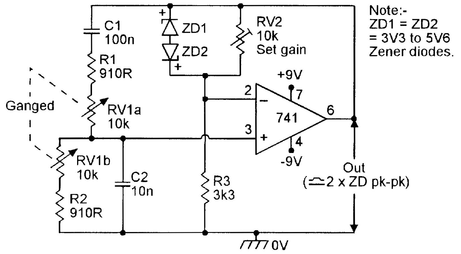 |
| Figure 6. Zener-regulated 150Hz-1.5kHz Wien Bridge oscillator. |
This ‘limiting’ technique typically results in the generation of 1% to 2% THD on the sinewave output when RV2 is set so that oscillation is maintained over the whole frequency band. The maximum peak-to-peak output of each circuit is roughly double the breakdown voltage of its diode regulator element. In the Figure 5 circuit, the diodes start to conduct at 500mV, so the circuit gives a peak-to-peak output of about 1V0; in the Figure 6 circuit, the zener diodes are connected back-to-back and may have values as high as 5V6, giving a pk-to-pk output of about 12V.
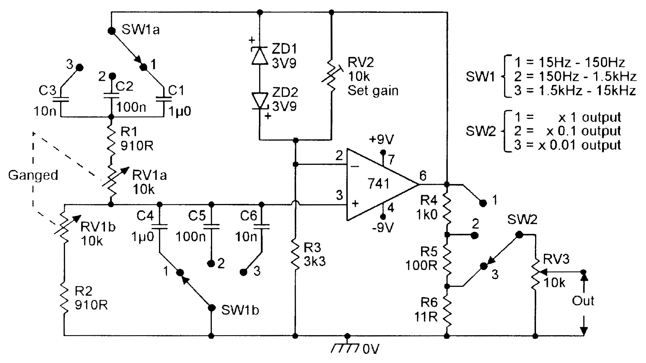 |
| Figure 7. Three-decade (15Hz-15kHz) Wien Bridge oscillator. |
The frequency ranges of the above circuits can be altered by changing the C1 and C2 values; increasing the values by a decade reduces the frequency by a decade. Figure 7 shows the circuit of a variable-frequency Wien oscillator that covers the range 15Hz to 15kHz in three switched decade ranges. The circuit uses zener diode amplitude stabilization; its output amplitude is variable via both switched and fully-variable attenuators. Note that the maximum useful operating frequency of this type of circuit is restricted by the slew-rate limitations of the op-amp. The limit is about 25kHz with a 741 op-amp, or about 70kHz with a CA3140.
A TWIN-T OSCILLATOR
Another way of making a sinewave oscillator is to wire a Twin-T network between the output and input of an inverting op-amp, as shown in the diode-regulated 1kHz oscillator circuit in Figure 8. The Twin-T network comprises R1-R2-R3-RV1 and C1-C2-C3, and in a ‘balanced’ circuit; these components are in the ratios R1 = R2 = 2 (R3 + RV1), and C1 = C2 = C3/2.
When the network is perfectly balanced, it acts as a frequency-dependent attenuator that gives zero output at a center frequency (fO) of 1/2 π R1.C1, and a finite output at all other frequencies. When the network is imperfectly balanced, it gives a minimal but finite output at fO, and the phase of this output depends on the direction of the imbalance: if the imbalance is caused by (R3 + RV1) being too low in value, the output phase is inverted relative to the input.
 |
| Figure 8. Diode-regulated 1kHz Twin-T oscillator. |
In Figure 8, the 1kHz Twin-T network is wired between the output and the inverting input of the op-amp, and RV1 is critically adjusted so that the Twin-T gives a small inverted output at fO; under this condition zero overall phase inversion occurs around the feedback loop, and the circuit oscillates at the 1kHz center frequency.
In practice, RV1 is adjusted so that oscillation is barely sustained and, under this condition, the sinewave output distortion is less than 1% THD. Automatic amplitude control is provided via D1, which provides a feedback signal via RV2; this diode progressively conducts and reduces the circuit gain when the diode forward voltage exceeds 500mV.
To set up the Figure 8 circuit, first set RV2 slider to the op-amp output and adjust RV1 so that oscillation is just sustained; under this condition, the output signal has an amplitude of about 500mV pk-to-pk. RV2 then enables the output signal to be varied between 170mV and 3V0 RMS. Note that Twin-T circuits make good fixed-frequency sinewave oscillators, but are not suitable for variable-frequency use, due to the difficulties of varying three or four network components simultaneously.
SQUAREWAVE GENERATORS
 |
| Figure 9. Basic relaxation oscillator circuit. |
Figure 9 shows a basic op-amp relaxation oscillator or squarewave generator using dual (split) power supplies. Its circuit action is such that C1 alternately charges and discharges (via R1) towards an ‘aiming’ or reference voltage set by R2-R3, and each time C1 reaches this aiming voltage, a regenerative comparator action occurs and makes the op-amp output switch state (to positive or negative saturation); this action produces a symmetrical squarewave at the op-amp’s output and a non-linear trianglewave across C1.
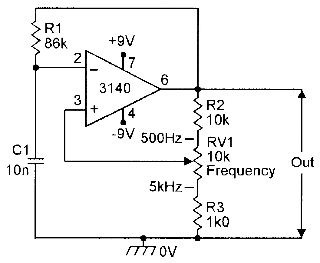 |
| Figure 10. Simple 500Hz-5kHz squarewave generator. |
The operating frequency can be varied by altering either the R1 or C1 values or the R2-R3 ratios; this circuit is thus quite versatile. A fast op-amp such as the CA3140 should be used if good output rise and fall times are needed from the squarewave.
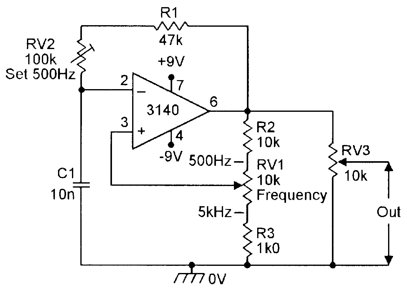 |
| Figure 11. Improved 500Hz-5kHz squarewave generator. |
Figure 10 shows the basic circuit adapted to make a practical 500Hz to 5kHz squarewave generator, with frequency variation obtained by altering the R2-RV1-R3 attenuator ratio. Figure 11 shows the circuit improved by using RV2 to pre-set the range of the RV1 frequency control, and by using RV3 as an output amplitude control.
 |
| Figure 12. Four-decade, 2Hz-20kHz, squarewave generator. |
Figure 12 shows how the above circuit can be modified to make a general-purpose squarewave generator that covers the 2Hz to 20kHz range in four switched decade ranges. Pre-set pots RV1 to RV4 are used to precisely set the minimum frequency of the 2Hz to 20Hz, 20Hz to 200Hz, 20Hz to 2kHz, and 2kHz to 20kHz ranges, respectively.
VARIABLE SYMMETRY
In the basic Figure 9 circuit, C1 alternately charges and discharges via R1, and the circuit generates a symmetrical squarewave output. The circuit can easily be modified to give a variable-symmetry output by providing C1 with alternate charge and discharge paths, as shown in Figures 13 and 14.
 |
| Figure 13. Squarewave generator with variable M/S-ratio and frequency. |
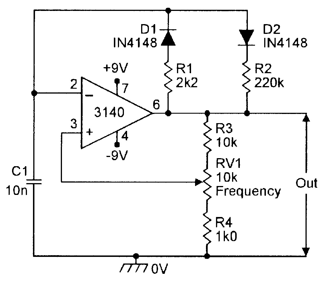
In the Figure 13 circuit, the mark/space (M/S) ratio of the output waveform is fully variable from 11:1 to 1:11 via RV1, and the frequency is variable from 650Hz to 6.5kHz via RV2. The circuit action is such that C1 alternately charges up via R1-D1 and the left-hand side of RV1, and discharges via R1-D2 and the right-hand side of RV1, to provide a variable-symmetry output. In practice, variation of RV1 has negligible effect on the operating frequency of the circuit.
 |
| Figure 14. Variable-frequency narrow-pulse generator. |
In the Figure 14 circuit, the mark period is determined by C1-D1-R1, and the space period by C1-D2-R2; these periods differ by a factor of 100, so the circuit generates a narrow pulse waveform. The pulse frequency is variable from 300Hz to 3kHz via RV1.
TRIANGLE-SQUARE GENERATION
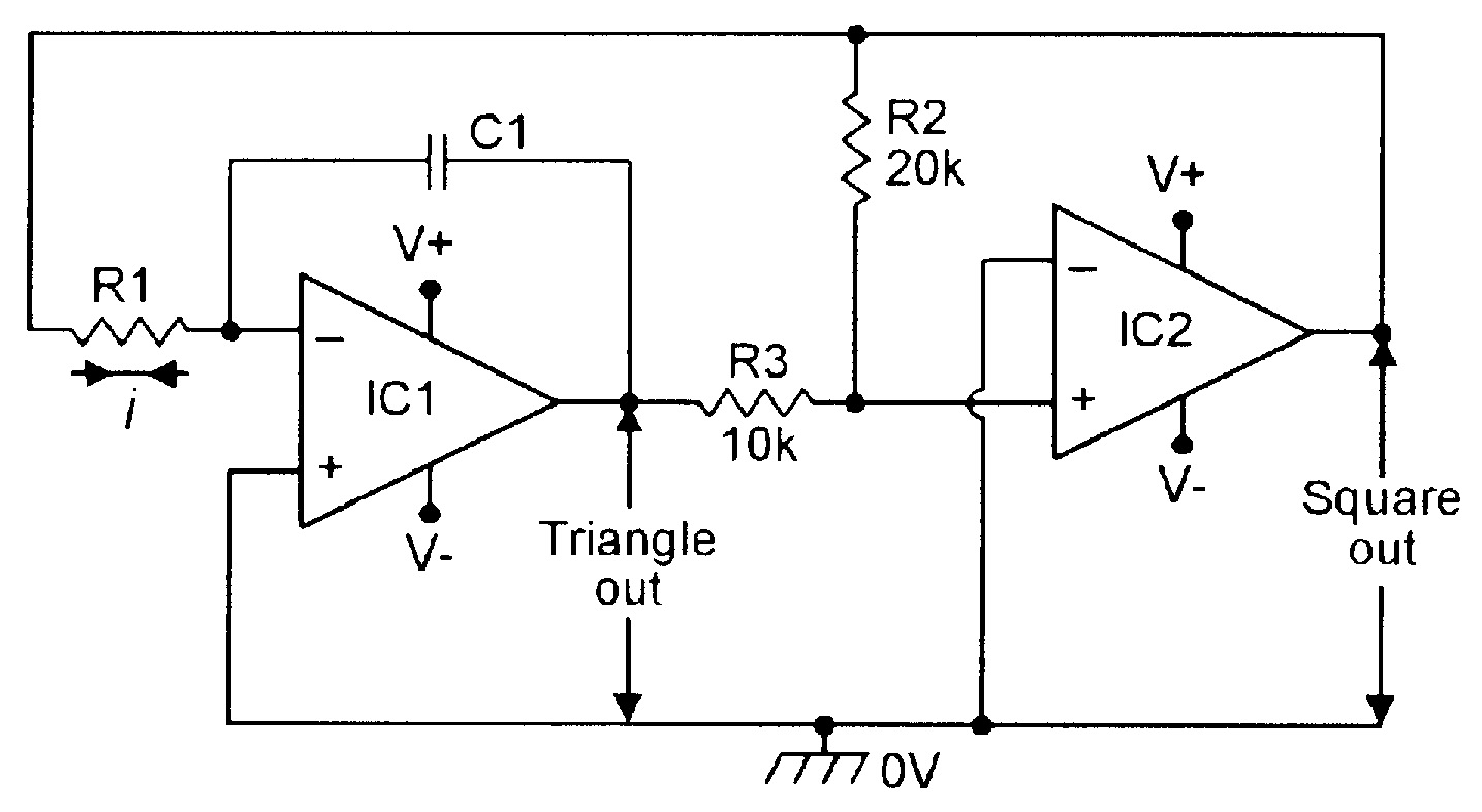
Figure 15 shows the basic circuit of a function generator that simultaneously generates a linear triangle and a square waveform, using two op-amps. IC1 is wired as an integrator, driven from the output of IC2, and IC2 is wired as a differential voltage comparator, driven from the output of IC1 via potential divider R2-R3, which is connected between the outputs of IC1 and IC2. The squarewave output of IC2 switches alternately between positive and negative saturation. The circuit functions as follows.
Suppose initially that the output of IC1 is positive and the output of IC2 has just switched to positive saturation. The inverting input of IC1 is a virtual earth point, so a current (i) of +Vsat/R1 flows into R1, causing the output of IC1 to start to swing down linearly at a rate of i/C1 volts per second. This output is fed — via the R2-R3 divider — to the non-inverting input of IC2, which has its inverting terminal referenced directly to ground.
Consequently, the output of IC1 swings linearly to a negative value until the R2-R3 junction voltage falls to zero, at which point IC2 enters a regenerative switching phase, in which its output abruptly switches to negative saturation. This reverses the inputs of IC1 and IC2, so IC1 output starts to rise linearly, until it reaches a positive value at which the R2-R3 junction voltage reaches the zero volts reference value, initiating another switching action. The whole process then repeats add infinitum.
 |
| Figure 15. Basic triangle/square function generator. |
Important points to note about the Figure 15 circuit are that the pk-to-pk amplitude of the linear triangle waveform is controlled by the R2-R3 ratio, and that the circuit’s operating frequency can be altered by changing either the ratios of R2-R3, the values of R1 or C1, or by feeding R1 from a potential divider connected to the output of IC2 (rather than directly from IC2 output. Figure 16 shows the practical circuit of a variable-frequency triangle/square generator that uses the latter technique.
 |
| Figure 16. 100Hz-1kHz triangle/square function generator. |
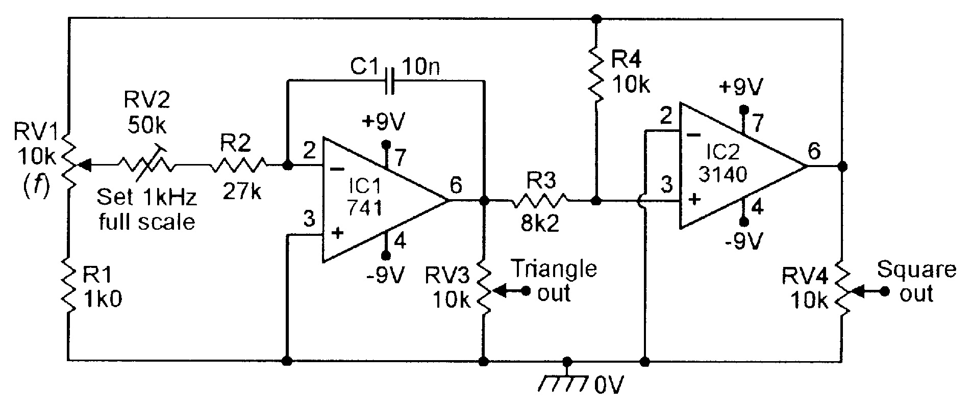
In Figure 16, the input current of C1 (obtained from RV2-R2) can be varied over a 10:1 range via RV1, enabling the frequency to be varied from 100Hz to 1kHz; RV2 enables the full-scale frequency to be set to precisely 1kHz. The amplitude of the linear triangle output waveform is fully variable via RV3, and of the squarewave via RV4.
 |
| Figure 17. 100Hz-1kHz ramp/rectangle generator with variable slope-M/S ratio. |
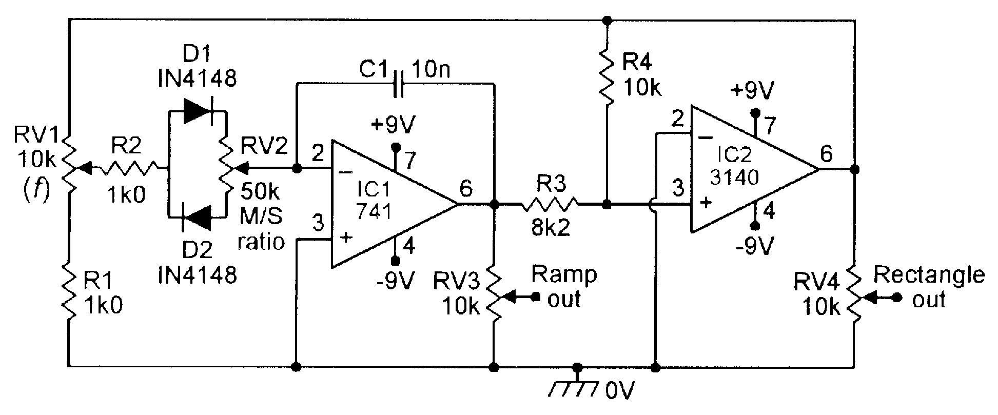
The Figure 16 circuit generates symmetrical output waveforms, since C1 alternately charges and discharges at equal current values (determined by RV2-R2, etc.). Figure 17 shows how the circuit can be modified to make a variable-symmetry ramp/rectangle generator, in which the slope is variable via RV2. C1 alternately charges via R2-D1 and the upper half of RV2, and discharges via R2-D2 and the lower half of RV2.
SWITCHING CIRCUITS
To conclude this month’s edition of the ‘OP-AMP COOKBOOK,’ Figures 18 to 20 show three ways of using op-amps as simple regenerative switches. Figure 18 shows the connections for making a simple manually-triggered bistable circuit. Note here that the inverting terminal of the op-amp is tied to ground via R1, and the non-inverting terminal is tied directly to the output. The circuit operates as follows.
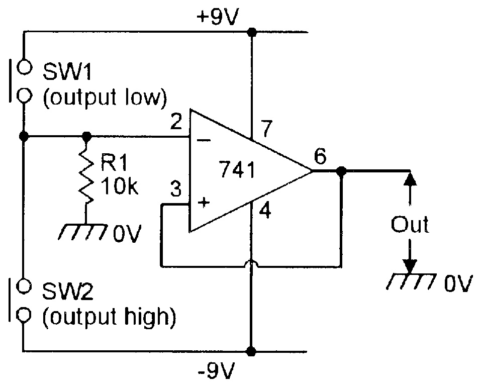 |
| Figure 18. Simple manually-triggered bistable. |
Normally, SW1 and SW2 are open. If SW1 is briefly closed, the op-amp inverting terminal is momentarily pulled high and the output is driven to negative saturation; consequently, when SW1 is released again, the inverting terminal returns to zero volts, but the output and the non-inverting terminals remain in negative saturation.
 |
| Figure 19. Single-supply manually-triggered bistable. |
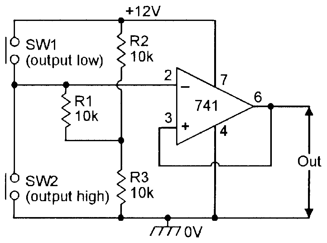
The output remains in this state until SW2 is briefly closed, at which point, the op-amp output switches to positive saturation, and locks into this state until SW1 is again operated. The circuit thus gives a bistable form of operation. Figure 19 shows how the circuit can be modified for operation from a single-ended power supply. In this case, the op-amp’s inverting terminal is biased to half-supply volts via R1 and the R2-R3 potential divider.
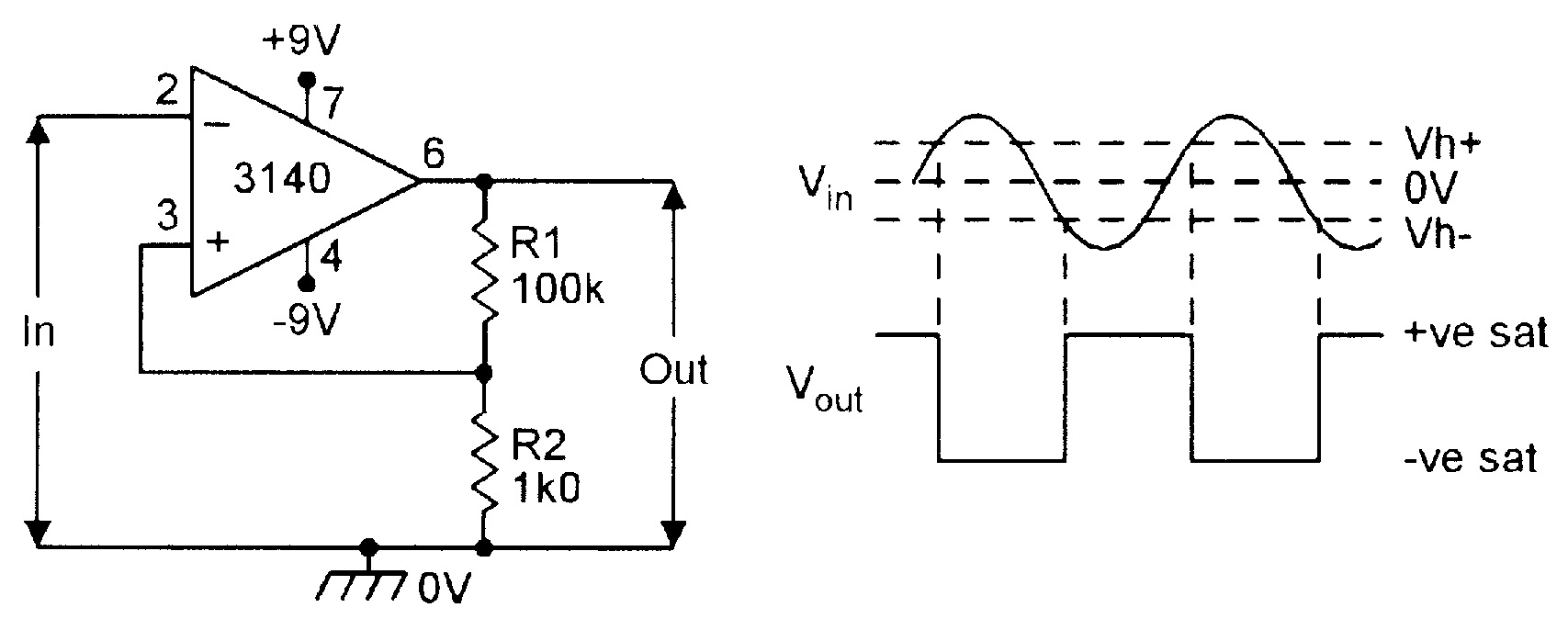 |
| Figure 20. Schmitt trigger. |
Finally, Figure 20 shows how to connect an op-amp as a Schmitt trigger, which can (for example), be used to convert a sinewave input into a squarewave output. The circuit operates as follows.
Suppose initially that the op-amp output is at a positive saturation value of 8V0. Under this condition, the R1-R2 divider feeds a positive reference voltage of 8V x (R1+R2)/R2 (= about 80mV in this case) to the op-amp’s non-inverting pin. Consequently, the output remains in this state until the input rises to a value equal to this voltage, at which point the op-amp output switches regeneratively to a negative saturation level of -8V0, feeding a reference voltage of -80mV to the non-inverting input.
The output remains in this state until the input signal falls to -80mV, at which point, the op-amp output switches regeneratively back to the positive saturation level. The process then repeats add infinitum. The actual switching levels can be altered by changing the R1 value. NV
Next time, we'll take a look at practical op-amp instrumentation and test-gear circuits in the final installment of this four-part series.