A conventional op-amp (operational amplifier) can be simply described as a high-gain direct-coupled amplifier 'block' that has a single output terminal, but has both inverting and non-inverting input terminals, thus enabling the device to function as either an inverting, non-inverting, or differential amplifier. Op-amps are very versatile devices. When coupled to suitable feedback networks, they can be used to make precision AC and DC amplifiers and filters, oscillators, level switches, and comparators, etc.
Three basic types of operational amplifiers are readily available. The most important of these is the conventional 'voltage-in, voltage-out' op-amp (typified by the popular 741 and CA3140 ICs), and this four-part mini-series takes an in-depth look at the operating principles and practical applications of this type of device. The other two basic types of op-amps are the current-differencing or Norton op-amp (typified by the LM3900), and the operational transconductance amplifier or OTA (typified by the CA3080 and LM13700); these two devices will be described in some future articles.
OP-AMP BASICS
In its simplest form, a conventional op-amp consists of a differential amplifier (bipolar or FET) followed by offset compensation and output stages, as shown in Figure 1. All of these elements are integrated on a single chip and housed in an IC package. The differential amplifier has inverting and non-inverting input terminals, and has a high-impedance (constant-current) tail to give a high input impedance and good common-mode signal rejection. It also has a high-impedance collector (or drain) load, to give a large amount of signal-voltage gain (typically about 100dB).
 |
| FIGURE 1. Simplified op-amp equivalent circuit. |
The output of the differential amplifier is fed to the circuit's output stage via an offset compensation network which — when the op-amp is suitably powered — causes the op-amp output to center on zero volts when both input terminals are tied to zero volts. The output stage takes the form of a complementary emitter follower, and gives a low-impedance output.
 |
| FIGURE 2. Basic symbol (a) and supply connections (b) of an op-amp. |
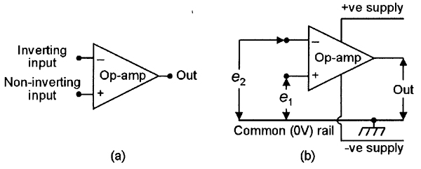
Conventional op-amps are represented by the standard symbol shown in Figure 2(a). They are normally powered from split supplies, as shown in Figure 2(b), providing positive, negative, and common (zero volt) supply rails, enabling the op-amp output to swing either side of the zero volts value and to be set to zero when the differential input voltage is zero. They can, however, also be powered from single-ended supplies, if required.
BASIC CONFIGURATIONS
The output signal of an op-amp is proportional to the differential signal voltage between its two input terminals and, at low audio frequencies, is given by:
eout = Ao(e1 - e2)
where Ao is the low frequency open-loop voltage gain of the op-amp (typically 100dB, or x100,000, e1 is the signal voltage at the non-inverting input terminal, and e2 is the signal voltage at the inverting input terminal).
Thus, an op-amp can be used as a high-gain inverting DC amplifier by grounding its non-inverting terminal and feeding the input signal to the inverting terminal, as shown in Figure 3(a). Alternatively, it can be used as a non-inverting DC amplifier by reversing the two input connections, as shown in Figure 3(b), or as a differential DC amplifier by feeding the two input signals to the op-amp as shown in Figure 3(c). Note in the latter case that if identical signals are fed to both input terminals, the op-amp should — ideally — give zero signal output.
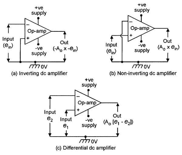 |
| FIGURE 3. Methods of using the op-amp as a high gain, open loop, linear DC amplifier. |
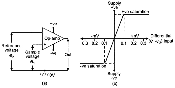
The voltage gains of the Figure 3 circuits depend on the individual op-amp open-loop voltage gains, and these are subject to wide variations between individual devices. One special application of the 'open-loop' op-amp is as a differential voltage comparator, one version of which is shown in Figure 4(a). Here, a fixed reference voltage is applied to the inverting terminal and a variable test or sample voltage is fed to the non-inverting terminal. Because of the very high open-loop voltage gain of the op-amp, the output is driven to positive saturation (close to the positive rail value) when the sample voltage is more than a few hundred microvolts above the reference voltage, and to negative saturation (close to the negative supply rail value) when the sample is more than a few hundred microvolts below the reference value.
 |
| FIGURE 4. Circuit (a) and transfer characteristics (b) of a simple differential voltage comparator. |
|
| |
Figure 4(b) shows the voltage transfer characteristics of the above circuit. Note that it is the magnitude of the input differential voltage that determines the magnitude of the output voltage, and that the absolute values of input voltage are of little importance. Thus, if a 2V0 reference is used and a differential voltage of only 200mV is needed to swing the output from a negative to a positive saturation level, this change can be caused by a shift of only 0.01% on a 2V0 signal applied to the sample input. The circuit thus functions as a precision voltage comparator or balance detector.
CLOSED-LOOP AMPLIFIERS
The most useful way of using an op-amp as a linear amplifier is to connect it in the closed-loop mode, with negative feedback applied from the output to the input, as shown in the basic DC-coupled circuits of Figure 5. This technique enables the overall gain of each circuit to be precisely controlled by the values of the external feedback components, almost irrespective of the op-amp characteristics (provided that the open-loop gain, Ao, is large relative to the closed-loop gain, A).
 |
| FIGURE 5. Closed-loop linear amplifier circuits. |
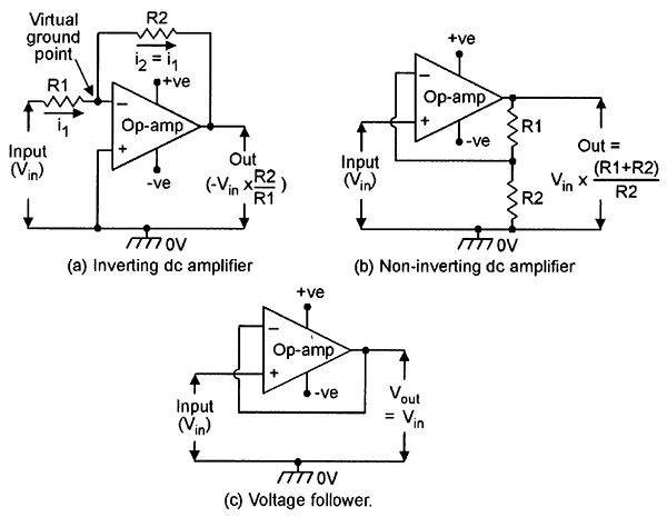
Figure 5(a) shows how to wire the op-amp as a fixed-gain inverting DC amplifier. Here, the gain (A) of the circuit is dictated by the ratios of R1 and R2 and equals R2/R1, and the input impedance of the circuit equals the R1 value; the circuit can thus easily be designed to give any desired values of gain and input impedance.
Note in Figure 5(a) that although R1 and R2 control the gain of the complete circuit, they have no effect on the parameters of the actual op-amp. Thus, the inverting terminal still has a very high input impedance, and negligible signal current flows into the terminal. Consequently, virtually all of the R1 signal current also flows in R2, and signal currents i1 and i2 can (for most practical purposes) be regarded as being equal, as shown in the diagram. Also note that R2 has an apparent value of R2/A when looked at from the inverting terminal, and the R1-R2 junction thus appears as a low-impedance 'virtual ground' point.
Figure 5(b) shows how to connect the op-amp as a fixed-gain non-inverting amplifier. In this case, the voltage gain equals (R1+R2)/R2, and the input impedance approximates (Ao/A)Zin, where Zin is the open-loop input impedance of the op-amp. The above circuit can be made to function as a precision voltage follower by connecting it as a unity-gain non-inverting amplifier, as shown in Figure 5(c), where the op-amp operates with 100% negative feedback. In this case, the input and output signal voltages are identical, but the input impedance of the circuit is very high, approximating Ao x Zin.
The basic op-amp circuits of Figures 5(a) to 5(c) are shown as DC amplifiers, but can readily be adapted for AC use by AC-coupling their inputs. Op-amps also have many applications other than as simple linear amplifiers. They can be made to function in precision phase splitters, as adders or subtractors, as active filters or selective amplifiers, and as oscillators or multivibrators, etc. Some of these applications are shown later in this article; in the meantime, let's look at some important op-amp parameters.
OP-AMP PARAMETERS
An ideal op-amp would have infinite values of input impedance, gain, and bandwidth, and have zero output impedance and give perfect tracking between input and output. Practical op-amps fall short of all of these ideals. Consequently, various performance parameters are detailed in op-amp data sheets, and indicate the measure of 'goodness' of a particular device. The most important of these parameters are detailed below.
- Ao (open-loop voltage gain). This is the low-frequency voltage gain occurring between the input and output terminals of the op-amp, and may be expressed in direct terms or in terms of dB. Typical figures are x100,000, or 100dB.
- ZIN (input impedance). This is the resistive impedance looking directly into the input terminals of the op-amp when used open-loop. Typical values are 1M0 for op-amps with bipolar input stages, and a million megohms for FET-input op-amps.
- Zo (output impedance). This is the resistive output impedance of the basic op-amp when used open-loop. Values of a few hundred ohms are typical of most op-amps.
- Ib (input bias current). The input terminals of all op-amps sink or source finite currents when biased for linear operation. The magnitude of this current is denoted by Ib, and is typically a fraction of a microamp in bipolar op-amps, and a few picoamps in FET types.
- VS (supply voltage range). Op-amps are usually operated from split (+ve and -ve) supply rails, which must be within maximum and minimum limits. If voltages are too high, the op-amp may be damaged and, if too low, the op-amp will not function correctly. Typical limits are ±3V to ±15V.
- Vi(max) (input voltage range). Most op-amps will only operate correctly if their input terminal voltages are below the supply line values. Typically, Vi(max) is one or two volts less than VS.
- Vio (differential input offset voltage). Ideally, an op-amp's output should be zero when both inputs are grounded, but in practice, slight imbalances within the op-amp cause it to act as though a small offset or bias voltage exists on its inputs under this condition. Typically, this Vio has a value of only a few mV, but when this voltage is amplified by the gain of the circuit in which the op-amp is used, it may be sufficient to drive the op-amp output well away from the 'zero' value. Because of this, most op-amps have some facility for externally nulling out the effects of this offset voltage.
- CMMR (common mode rejection ratio). An op-amp produces an output proportional to the difference between the signals on its two input terminals. Ideally, it should give zero output if identical signals are applied to both inputs simultaneously, i.e., in common mode. In practice, such signals do not entirely cancel out within the op-amp, and produce a small output signal. The ability of an op-amp to reject common mode signals is usually expressed in terms of CMMR, i.e., the ratio of the op-amp's gain with differential signals versus the gain with common mode signals. CMMR values of 90dB are typical of most op-amps.
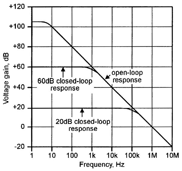 |
FIGURE 6. Typical frequency response curve of the 741op-amp.
|
- fT (transition frequency). An op-amp typically gives a low-frequency voltage gain of about 100dB, and in the interest of stability, its open-loop frequency response is internally tailored so that the gain falls off at a rate of 6dB/octave (= 20dB/decade), eventually falling to unity (0dB) at a transition frequency denoted fT. Figure 6 shows the typical response curve of the type 741 op-amp, which has an fT value of 1MHz and a low-frequency gain of 106dB. Note that, when the op-amp is used in a closed loop amplifier circuit, the circuit's bandwidth depends on the closed-loop gain. Thus, in Figure 6, the circuit has a bandwidth of only 1kHz at a gain of 60dB, or 100kHz at a gain of 20dB. The fT figure can thus be used to represent a gain-bandwidth product.
 |
FIGURE 7. Effect of slew-rate limiting on the output of an op-amp fed with a squarewave input.
|
- Slew rate. As well as being subject to normal bandwidth limitations, op-amps are also subject to a phenomenon known as slew rate limiting, which has the effect of limiting the maximum rate of change of voltage at the op-amp's output. Figure 7 shows the effect that slew-rate limiting can have on the output of an op-amp that is fed with a squarewave input. Slew rate is normally specified in terms of volts per microsecond, and values in the range 1V/mS to 10V/mS are usual with most popular types of op-amp. One effect of slew rate limiting is to make a greater bandwidth available to small-amplitude output signals than to large-amplitude output signals.
PRACTICAL OP-AMPS
Practical op-amps are available in a variety of types of IC construction (bipolar, MOSFET, JFET, etc.), and in a variety of types of packaging (plastic DIL, metal-can TO5, etc.). Some of these packages house two or four op-amps, all sharing common supply line connections. Figure 8 gives parameter and outline details of eight popular 'single' op-amp types, all of which use eight-pin DIL (DIP) packaging.
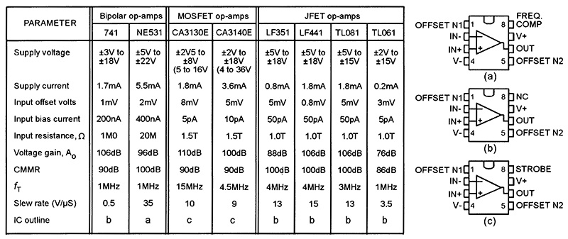 |
| FIGURE 8. Parameter and outline details of eight popular 'single' op-amp types. |
The 741 and NE531 are bipolar types. The 741 is a popular general-purpose op-amp featuring internal frequency compensation and full overload protection on inputs and outputs. The NE531 is a high-performance type with very high slew rate capability; an external compensation capacitor (100pF) — wired between pins 6 and 8 — is needed for stability, but can be reduced to a very low value (1.8pF) to give a very wide bandwidth at high gain.
The CA3130 and CA3140 are MOSFET-input type op-amps that can operate from single or dual power supplies, can sense inputs down to the negative supply rail value, have ultra-high input impedances, and have outputs that can be strobed; the CA3130 has a CMOS output stage, and an external compensation capacitor (typically 47pF) between pins 1 and 8 permits adjustment of bandwidth characteristics; the CA3140 has a bipolar output stage and is internally compensated.
The LF351, LF411, TL081, and TL061 JFET types can be used as direct replacements for the 741 in most applications; the TL061 is a low-power version of the TL081.
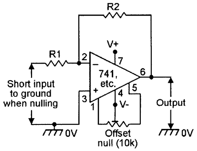
OFFSET NULLING
All of the above op-amps are provided with an offset nulling facility, to enable the output to be set to precisely zero with zero input, and this is usually achieved by wiring a 10k pot between pins 1 and 5 and connecting the pot slider (either directly or via a 4k7 range-limiting resistor) to the negative supply rail (pin 4), as shown in Figure 9. In the case of the CA3130, a 100k offset nulling pot must be used.
 |
| FIGURE 9. Typical offset nulling system. |
APPLICATIONS ROUNDUP
Operational amplifiers are very versatile devices, and can be used in an almost infinite variety of linear and switching applications. Figures 10 to 22 show a small selection of basic 'applications' circuits that can be used, and which will be looked at in greater detail in the remaining three episodes of this 'Op-Amp' mini-series. In most of these diagrams, the supply line connections have been omitted for clarity.
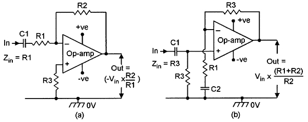 |
| FIGURE 10. Basic inverting (a) and non-inverting (b) AC amplifier circuits. |
Figure 10 shows basic ways of using op-amps to make fixed-gain inverting or non-inverting AC amplifiers. In both cases, the gain and the input impedance of the circuit can be precisely controlled by suitable component value selection.
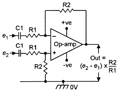
Figure 11 shows how to make a differential or difference amplifier with a gain equal to R2/R1; if R1 and R2 have equal values, the circuit acts as an analog subtractor.
 |
 |
| FIGURE 11. Differential amplifier or analog subtractor. |
FIGURE 12. Inverting analog adder or audio mixer. |
Figure 12 shows the circuit of an inverting 'adder' or audio mixer; if R1 and R2 have equal values, the inverting output is equal to the sum of the input voltages.
 |
| FIGURE 13. High-pass (a) and low-pass (b) second-order active filters. |
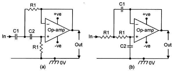
Op-amps can be made to act as precision active filters by wiring suitable filters into their feedback networks. Figure 13 shows the basic connections for making second-order high-pass and low-pass filters; these circuits give roll-offs of 12dB/octave. Next month's episode of this mini-series will show more sophisticated versions of these basic circuits.
 |
 |
 |
| FIGURE 14. Supply-line splitter. |
FIGURE 15. Adjustable-voltage reference. |
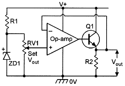
FIGURE 16. Adjustable-voltage DC power supply. |
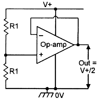
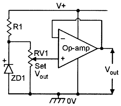
Figures 14 to 16 show some useful applications of the basic voltage follower or unity-gain non-inverting DC amplifier. The Figure 14 circuit acts as a supply line splitter, and is useful for generating split DC supplies from single-ended ones. Figure 15 acts as a semi-precision variable voltage reference, and Figure 16 shows how the output current drive can be boosted so that the circuit acts as a variable voltage supply.
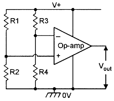 |
| FIGURE 17. Bridge-balancing detector/switch. |
Figure 17 shows the basic circuit of a DC bridge-balancing detector, in which the output swings high when the inverting pin voltage is above that of the non-inverting pin, and vice versa. This circuit can be made to function as a precision opto- or thermo-switch by replacing one of the bridge resistors with an LDR or thermistor.
 |
 |
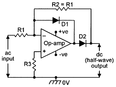
| FIGURE 18. Precision half-wave rectifier. |
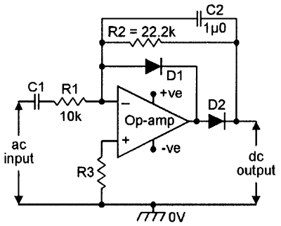
FIGURE 19. Precision half-wave AD/DC converter. |
Figures 18 and 19 show how to make precision half-wave rectifiers and AC/DC converters. These are very useful instrumentation circuits.
 |
 |
 |
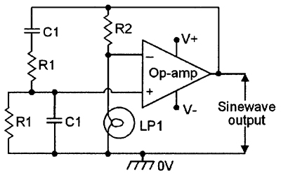
| FIGURE 20. Wien-bridge sinewave generator. |
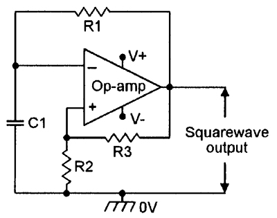
FIGURE 21. Free-running multivibrator. |
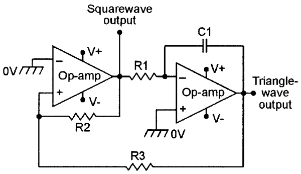
FIGURE 22. Sine/square function generator. |
Finally, to complete this opening episode, Figures 20 to 22 show some useful waveform generator circuits. The Figure 20 design uses a Wien bridge network to generate a good sinewave; amplitude stabilization is obtained via a low-current lamp (or thermistor). Figure 21 is a very useful squarewave generator circuit, in which the frequency can be controlled via any one of the passive component values. The frequency of the Figure 22 function generator circuit can also be controlled via any one of its passive component values, but this particular design generates both square and triangle output waveforms. NV