OPTOCOUPLER BASICS
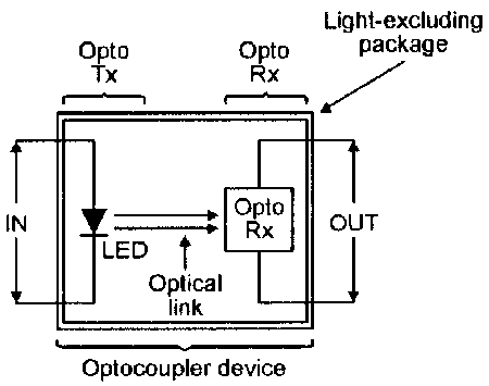
An optocoupler device can be simply described as a sealed, self-contained unit that houses independently-powered optical (light) Tx and Rx units, that can be coupled together optically. Figure 1 shows the basic form of such a device. Here, the Tx unit is a LED, but the Rx unit may take the form of a phototransistor, a photo-FET, an opto-triac, or some other type of photo-sensitive semiconductor element; the Tx and Rx units are housed closely together in a single, sealed package.
 |
 |
| FIGURE 1. Basic form of an optocoupler device. |
FIGURE 2. Basic form and application circuit of a typical optocoupler. |
Most modern optocoupler devices use a phototransistor as their Rx unit; such a device is known simply as an ‘optocoupler,’ since the input (the LED) and the output (the phototransistor) devices are optically coupled. Figure 2 shows the basic form of an optocoupler, together with a very simple application circuit. Here, when SW1 is open, no current flows in the LED, so no light falls on the face of Q1; Q1 passes virtually zero collector current under this condition, so zero voltage is developed across output resistor R2. Alternatively, when SW1 is closed, current flows through the LED via R1, and the resulting light falls on Q1’s face, causing the phototransistor to conduct and generate an output voltage across R2.
Major points to note about the Figure 2 optocoupler are that its output current is controlled by its input current, that a control circuit connected to its input can be electrically fully isolated from the output circuit, and that — since the input controls the output via a purely optical link — potential differences of hundreds of volts can safely exist between the input and output circuits. This ‘isolating’ characteristic is the main attraction of this type of optocoupler, which is generally known as an isolating optocoupler.
The simple application circuit of Figure 2 can be used with digital input/output signals only but, in practice, this basic circuit can easily be modified for use with analog input/output signals, as shown later in this article. Typical isolating optocoupler applications include low-voltage to high-voltage (or vice versa) signal coupling, interfacing of a computer’s output signals to external electronic circuitry or electric motors, etc., and interfacing of ground-referenced low-voltage circuitry to floating high-voltage circuitry driven directly from the main’s AC power lines, etc. Optocouplers can also be used to replace low-power relays and pulse transformers in many applications.
SPECIAL OPTOCOUPLERS
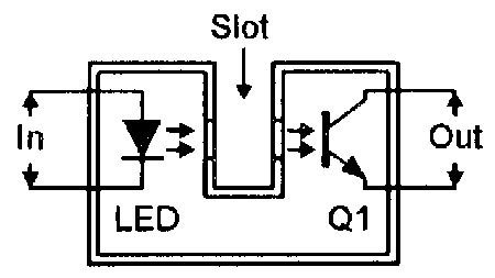
The Figure 2 device is a simple isolating optocoupler. Figures 3 and 4 show two other types of optocoupler. The device shown in Figure 3 is known as a slotted optocoupler, and has a slot molded into the package between the LED light source and the phototransistor light sensor. Here, light can normally pass from the LED to Q1 without significant attenuation by the slot. The optocoupling can, however, be completely blocked by placing an opaque object in the slot. The slotted optocoupler can thus be used in a variety of ‘presence’-detecting applications, including end-of-tape detection, limit switching, and liquid-level detection.
 |
 |
| FIGURE 3. Slotted optocoupler device. |
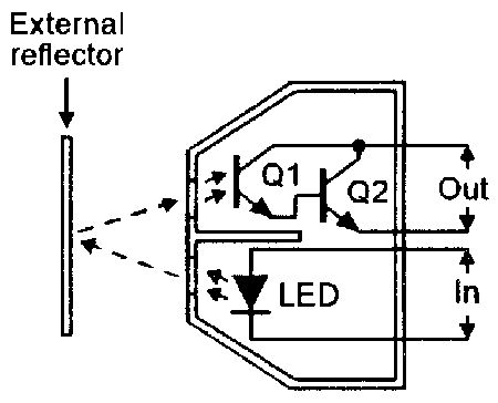
FIGURE 4. Reflective optocoupler. |
The device shown in Figure 4 is known as a reflective optocoupler. Here, the LED and Q1 are optically screened from each other within the package, and both face outwards (towards a common point) from the package. The construction is such that an optocoupled link can be set up by a reflective object (such as metallic paint or tape, or even smoke particles) sited a short distance outside the package, in line with both the LED and Q1. The reflective optocoupler can thus be used in applications such as tape-position detection, engine-shaft revolution counting or speed measurement, or smoke or fog detection, etc.
OPTOCOUPLER TRANSFER RATIOS
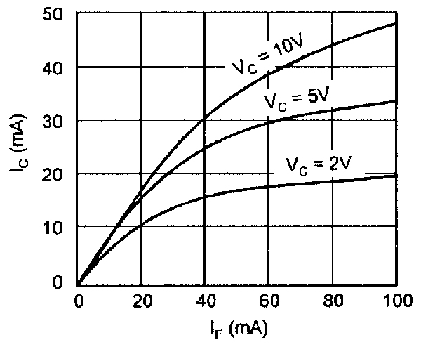 |
| FIGURE 5. Typical IC/IF characteristics of a simple optocoupler at various values of output-transistor collector voltage (VC). |
One of the most important parameters of an optocoupler device is its optocoupling efficiency and, to maximize this parameter, the LED and the phototransistor (which usually operate in the infrared range) are always closely matched spectrally.
The most convenient way of specifying optocoupling efficiency is to quote the output-to-input current transfer ratio (CTR) of the device, i.e., the ratio of the output collector current (IC) of the phototransistor, to the forward current (IF) of the LED. Thus, CTR = IC/IF. In practice, CTR may be expressed as a simple figure such as 0.5, or (by multiplying this figure by 100) as a percentage figure such as 50%.
Simple isolating optocouplers with single-transistor output stages have typical CTR values on the range of 20% to 100%; the actual CTR value depends (among other things) on the input and output current values of the device and on the supply voltage value (VC) of the phototransistor. Figure 5 shows three typical sets of output/input currents obtained at different VC values.
It should be noted that, because of variations in LED radiation efficiency and phototransistor current gains, the actual CTR values of individual optocouplers may vary significantly from the typical value. An optocoupler type with a typical CTR value of 60% may, for example, in fact have a true value in the range of 30% to 90% in an individual device.
OTHER PARAMETERS
Other important optocoupler parameters include the following.
ISOLATION VOLTAGE. This is the maximum permissible DC potential that can be allowed to exist between the input and output circuits. Typical values vary from 500V to 4kV.
VCE(MAX). This is the maximum allowable DC voltage that can be applied across the output transistor. Typical values vary from 20V to 80V.
IF(MAX). This is the maximum permissible DC current that can be allowed to flow in the input LED. Typical values vary from 40mA to 100mA.
BANDWIDTH. This is the typical maximum signal frequency that can be usefully passed through the optocoupler when the device is operated in its normal mode. Typical values vary from 20kHz to 500kHz, depending on the type of device construction.
PRACTICAL OPTOCOUPLERS
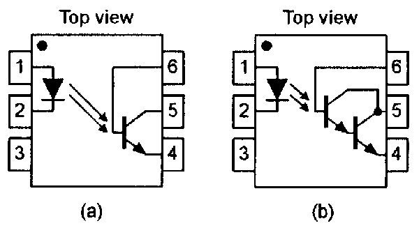 |
| FIGURE 6. Typical simple (a) and Darlington (b) isolating optocouplers. |
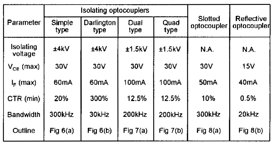
Optocouplers are produced by several manufacturers and are available in a variety of forms and styles. Simple optocouplers are widely available in six basic forms, which are illustrated in Figures 6 to 8. Four of these (Figures 6 and 7) are isolating optocouplers, and the remaining two are the slotted optocoupler (Figure 8(a)) and the reflective optocoupler (Figure 8(b)). The table of Figure 9 lists the typical parameter values of these six devices.
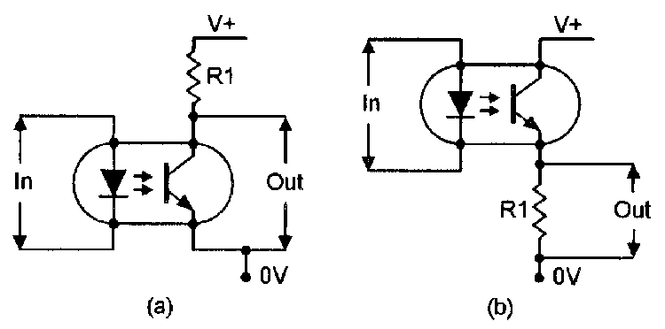
The simple isolating optocoupler (Figure 6(a)) uses a single phototransistor output stage and is usually housed in a six-pin package, with the base terminal of the phototransistor externally available. In normal use, the base is left open-circuit and, under this condition, the optocoupler has a minimum CTR value of 20% and a useful bandwidth of 300kHz. The phototransistor can, however, be converted to a photodiode by shorting the base (pin 6) and emitter (pin 4) terminals together; under this condition the CTR value falls to about 0.2%, but the bandwidth rises to about 30MHz.
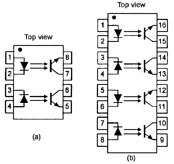 |
| FIGURE 7. Typical dual (a) and quad (b) isolating optocouplers. |
The Darlington optocoupler (Figure 6(b)) is also housed in a six-pin package and has its phototransistor base externally available. Because of the high current gain of the Darlington, this coupler has a typical minimum CTR value of about 300%, but has a useful bandwidth of only 30kHz.
The dual and quad optocouplers of Figure 7 use single-transistor output stages in which the base terminal is not externally available.
Note in all four isolating devices that the input pins are on one side of the package, and the output pins are on the other. This construction gives the maximum possible values of isolating voltage. Also note in the multichannel devices of Figure 7 that, although these devices have isolating voltages of 1.5kV, potentials greater than 500V should not be allowed to exist between adjacent channels.
 |
| FIGURE 8. Typical slotted (a) and reflective (b) optocouplers. |
Isolating voltage values are not specified for the slotted and reflective optocoupler devices of Figure 8. The Figure 8(a) device has a typical slot width of about 3mm, and uses a single output transistor to give an open slot minimum CTR value of 10% and a bandwidth of 300kHz.
Finally, the reflective optocoupler of Figure 8(b) uses a Darlington output stage and has a useful bandwidth of only 20kHz. Even so, the device has a typical minimum CTR value of only 0.5% at a reflective range of 5mm from a surface with a reflective efficiency of 90%, when the input LED is operated at its maximum current of 40mA.
 |
| FIGURE 9. Typical parameter values of the Figures 6 to 8 devices. |
OPTOCOUPLER USAGE NOTES
Optocouplers are very easy devices to use, with the input side being used in the manner of a normal LED and the output used in the manner of a normal phototransistor. The following notes give a summary of the salient usage points.
 |
 |
| FIGURE 10. The LED current must be limited by a series resistor, which can be connected to either the anode (a) or the cathode (b). |
FIGURE 11. The input LED can be protected against reverse voltages via an external diode. |
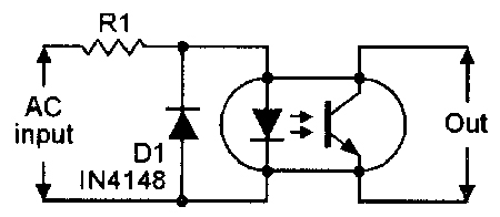
The input current to the optocoupler LED must be limited via a series-connected external resistor which, as shown in Figure 10, can be connected on either the anode or the cathode side of the LED. If the LED is to be driven from an AC source, or there is a possibility of a reverse voltage being applied across the LED, the LED must be protected from reverse voltages via an external diode connected as shown in Figure 11.
The phototransistor’s operating current can be converted into a voltage by wiring an external resistor in series with the collector of the device. This resistor can be connected to either the collector or the emitter of the phototransistor, as shown in Figure 12. The greater the value of this resistor, the greater is the sensitivity of the circuit, but the lower is its bandwidth.
 |
 |
| FIGURE 12. An external output resistor, wired in series with the phototransistor, can be connected to either the collector (a) or emitter (b). |
FIGURE 13. If its base is available, the phototransistor can be made to function as a photodiode (a), or its CTR values can be varied via RV1 (b). |
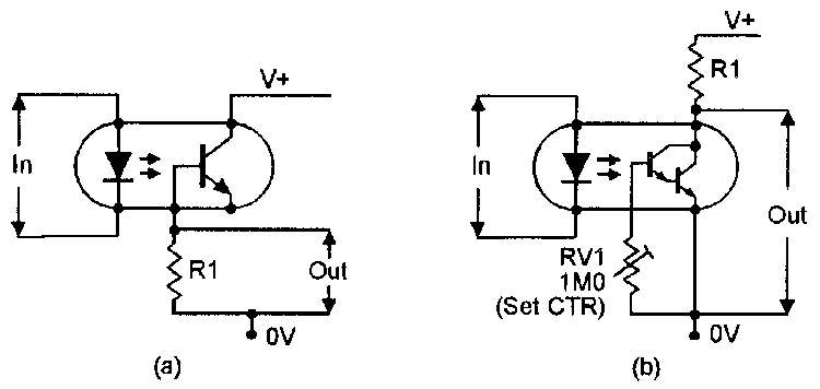
In normal use, the phototransistor is used with its base terminal open-circuit. If desired, however, the phototransistor can be converted into a photodiode by using the base terminal as shown in Figure 13(a) and ignoring the emitter terminal (or shorting it to the base). This connection results in a greatly increased bandwidth (typically 30MHz), but a greatly reduced CTR value (typically 0.2%).
Alternatively, the base terminal can be used to vary the CTR value of the optocoupler by wiring an external resistor (RV1) between the base and emitter, as shown in the Darlington example of Figure 13(b). With RV1 open-circuit, the CTR value is that of a normal Darlington optocoupler (typically 300% minimum); with RV1 short-circuit, the CTR value is that of a diode-connected phototransistor (typically about 0.2%).
DIGITAL INTERFACING
Optocoupler devices are ideally suited for use in digital interfacing applications in which the input and output circuits are driven by different power supplies. They can be used to interface digital ICs of the same family (TTL, CMOS, etc.) or digital ICs of different families, or to interface the digital outputs of home computers, etc., to motors, relays, and lamps, etc. This interfacing can be achieved using various special-purpose ‘digital interfacing’ optocoupler devices, or by using standard optocouplers; Figures 14 to 16 show circuits of the latter type.
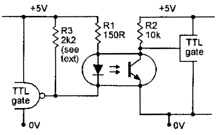
Figure 14 shows how to interface two TTL circuits, using an optocoupler circuit that provides a non-inverting action. Here, the optocoupler LED and current-limiting resistor R1 are connected between the 5V positive supply rail and the output-driving terminal of the TTL device (rather than between the TTL output and ground), because TTL outputs can usually sink a fairly high current (typically 16mA) but can source only a very low current (typically 400µA).
 |
 |
| FIGURE 14. TTL interface. |
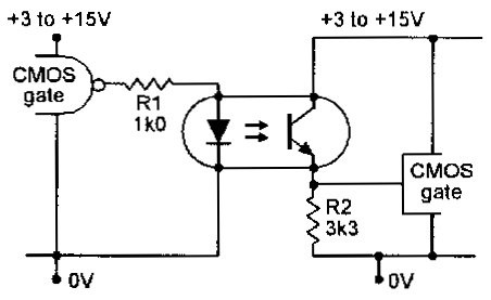
FIGURE 15. CMOS interface. |
The open-circuit output voltage of a TTL IC falls to less than 0.4V when in the logic-0 state, but may rise to only 2.4V in the logic-1 state if the IC is not fitted with an internal pull-up resistor. In such a case, the optocoupler LED current will not fall to zero when the TTL output is at logic-1. This snag is overcome in the Figure 14 circuit by fitting an external pull-up resistor (R3) as shown. The Figure 14 circuit’s optocoupler phototransistor is wired between the input and ground of the driven (right-hand) TTL IC because a TTL input needs to be pulled down to below 800mV at 1.6mA to ensure correct logic-0 operation.
CMOS IC outputs can source or sink currents (up to several mA) with equal ease. Consequently, these devices can be interfaced by using a sink configuration similar to that of Figure 14, or they can use the source configuration shown in Figure 15. In either case, the R2 value must be large enough to provide an output voltage swing that switches fully between the CMOS logic-0 and logic-1 states.
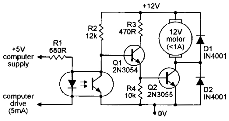 |
| FIGURE 16. Computer-driven DC motor. |
Figure 16 shows how the optocoupler can be used to interface a computer’s output signal (5V, 5mA) to a 12V DC motor that draws an operating current of less than 1A. With the computer output high, the optocoupler LED and phototransistor are both off, so the motor is driven on via Q1 and Q2. When the computer output goes low, the LED and phototransistor are driven on, so Q1-Q2 and the motor are cut off. The reverse of this action can be obtained by wiring the optocoupler’s output in series between R2 and Q1-base, so that Q1-Q2 and the motor turn on only when the computer output goes low.
ANALOG INTERFACING
An optocoupler can be used to interface analog signals from one circuit to another by setting up a standing current through the LED and then modulating this current with the analog signal. Figure 17 shows this technique used to make an audio-coupling circuit.
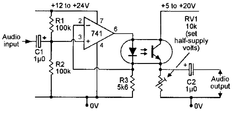 |
| FIGURE 17. Audio-coupling circuit. |
Here, the op-amp is connected in the unity-gain voltage follower mode, with the optocoupler LED wired into its negative feedback loop so that the voltage across R3 (and thus the current through the LED) precisely follows the voltage applied to the op-amp’s pin 3 non-inverting input terminal. This terminal is DC-biased at half-supply volts via the R1-R2 potential divider, and can be AC-modulated by an audio signal applied via C1. The quiescent LED current is set at 1 to 2 mA via R3.
On the output side of the optocoupler, a quiescent current is set up (by the optocoupler action) in the phototransistor, and causes a quiescent voltage to be set up across RV1, which should have its value adjusted to give a quiescent output value of half-supply voltage. The audio output signal appears across RV1 and is DC-decoupled via C2.
TRIAC INTERFACING
An ideal application for the optocoupler is that of interfacing the output of a low-voltage control circuit (possible with one side of its power supply grounded) to the input of a triac power-control circuit that is driven from the AC power lines and which can be used to control the power feed to lamps, heaters, and motors. Figure 18 shows an example of such a circuit; the figures in parenthesis show the component values that should be used if 115V AC (rather than 230V) supplies are used; the actual triac type must be chosen to suit individual load/supply requirements.
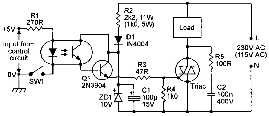 |
| FIGURE 18. Simple non-synchronous triac power switch with optocoupled input. |
The Figure 18 circuit gives a non-synchronous switching action in which the triac’s initial switch-on point is not synchronized to the AC power line waveform. Here, R2-D1-ZD1 and C1 are used to develop an AC-derived 10V DC supply, which can be fed to the triac gate via Q1 and hence be used to turn the triac on and off. Thus, when SW1 is open, the optocoupler is off, so zero base drive is applied to Q1, and the triac and load are off. When SW1 is closed, the optocoupler drives Q1 on and connects the 10V DC supply to the triac gate via R3, thus applying full AC mains power to the load.
OPTOCOUPLED SCRs and TRIACS
SCRs (silicon controlled rectifiers) and triacs are semiconductor power-switching devices that (like transistors) are inherently photosensitive. An optocoupled SCR is simply an SCR and an LED mounted in a single package, and an optocoupled triac is simply a triac and an LED mounted in a single package. Such devices are readily available, in both simple and complex forms; some sophisticated triac types incorporate interference-suppressing, zero-crossing switching circuitry in the package.
 |
 |
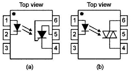
| FIGURE 19. Typical optocoupled SCR (a) and triac (b). |
FIGURE 20. Typical characteristics of optocoupled SCRs/triacs. |
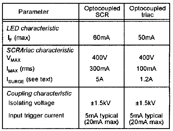
Figure 19(a) and 19(b) show the typical outlines of simple optocoupled SCRs and triacs (which are usually mounted in six-pin DIL packages); Figure 20 lists the typical parameters of these two particular devices, which have rather limited rms output-current ratings, the values being (in the examples shown) 300mA for the SCR and 100mA for the triac. The SCR device’s surge-current rating is 5A at a pulse width of 100µS and a duty cycle of less than 1%; the triac device’s surge rating is 1.2A at a pulse width of 10µS and a duty cycle of 10% maximum.
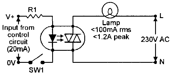
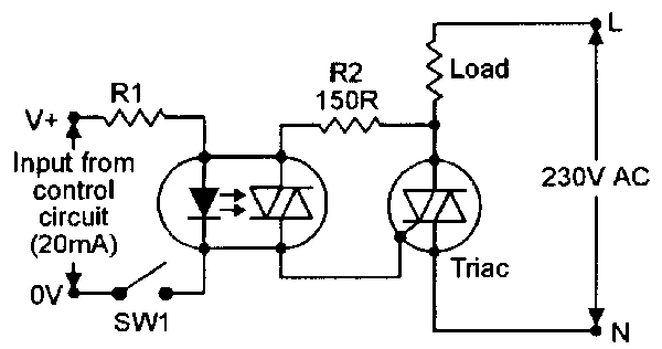
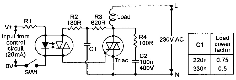
Optocoupled SCRs and triacs are very easy to use; the input LED is driven in the manner of a normal LED, and the SCR/triac is used like a normal low-power SCR/triac. Figures 21 to 23 show various ways of using an optocoupled triac; R1 should be chosen to pass an LED current of at least 20mA; all other component values are those used with a 230V AC supply.
In Figure 21, the triac is used to directly activate an AC line-powered filament lamp, which should have an rms rating of less than 100mA and a peak inrush current rating of less than 1.2A.
 |
 |
| FIGURE 21. Low-power lamp control. |
FIGURE 22. High-power control via a triac slave. |
Figure 22 shows how the optocoupled triac can be used to activate a slave triac and, thereby, activate a load of any desired power rating. This circuit is suitable for use only with non-inductive loads such as lamps and heating elements, using a triac of suitable rating.
 |
| FIGURE 23. Driving an inductive load. |
Finally, Figure 23 shows how the above circuit can be modified for use with inductive loads such as electric motors. The R2-C1-R3 network provides a degree of phase-shift to the triac gate-drive network, to ensure correct triac triggering action, and R4-C2 form a snubber network, to suppress rate-of-rise (rate) effects.
OPTOCOUPLED SSRs
An optocoupled solid-state relay (SSR) is a device that can be used as a superior replacement for many types of low-power electromechanical relays. Like a normal relay, it provides complete electrical isolation between its input and output circuits, and its output acts like an electrical switch that has a near-infinite resistance when open and a very low resistance when closed and which — when closed — can pass AC or DC currents with equal ease, without suffering ‘offset voltage’ losses.
Siemens are the present market leaders in the optocoupled SSR field. Their basic design has an IR LED input stage and a dual n-channel MOSFET output stage that (unlike a dual bipolar transistor stage) does not produce significant offset voltage drops when biased on. The IR LED’s output is coupled to the inputs of the MOSFETs via a bank of 25 photovoltaic diodes that — when illuminated — apply a 15V turn-on voltage to the MOSFET gates.
The simplest device in the Siemens range of optocoupled SSRs is the LH1540AT, which is housed in a six-pin package and has an output that acts as a normally-open (NO) single-pole switch. The device has an isolation voltage rating of 3.75kV and a maximum output load voltage rating of 350V. The LH1540AT has three output pins, which allow its two output IGFETs to be used in series for AC operation, or in parallel for DC operation.
When the input LED is passing a current of 5mA, the output can handle maximum load currents of 120mA and has a typical ‘on’ resistance of 25 ohms when used in the AC configuration, or 250mA and 5 ohms in the DC configuration. The device has typical on/off switching speeds of less than 1mS.
Other devices in the Siemens optocoupled SSRs range include ones that have outputs that act as single-pole or two-pole NC, NO, or change-over switches. NV