Basic operation and practical application circuits for SCRs.
An SCR (Silicon Controlled Rectifier) is a controllable medium- to high-power self-latching solid-state DC power switch. This article explains its basic operation and shows some practical ways of using it.
SCR basics
 |
 |
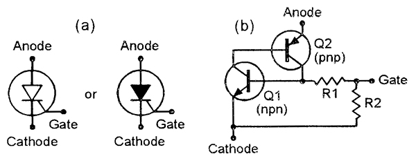
| FIGURE 1. Alternative SCR symbols (a) and SCR equivalent circuit (b). |
FIGURE 2. Basic way of using an SCR as a DC switch. |
An SCR is a four-layer PNPN silicon semiconductor device. It has three external terminals (anode, gate, and cathode) and uses the alternative symbols of Figure 1(a) and has the transistor equivalent circuit of Figure 1(b). Figure 2 shows the basic way of using the SCR as a DC switch, with the anode positive relative to the cathode, and the SCR controlled via its gate. The basic characteristics of the SCR can be understood with the aid of these diagrams, as follows:
- When power is first applied to the SCR by closing S1 in Figure 2, the SCR is 'blocked' and acts (between anode and cathode) like an open switch. This action is implied by Figure 1(b), i.e., Q2's base current is derived from Q1 collector, and Q1's base current is derived from either Q2 collector or the gate terminal; in the latter case, no base current is available, so both transistors are cut off, and only a small leakage current flows from anode to cathode.
- The SCR can be turned on and made to act like a forward-biased silicon rectifier by briefly applying gate current to it via S2; the SCR quickly (in a few microseconds) self-latches into the on state under this condition, and stays on even when the gate drive is removed. This action is implied by Figure 1(b); the initial gate current turns Q1 on, and Q1's collector current turns Q2 on, and Q2's collector current then holds Q1 on even when the gate drive is removed: a 'saturation' potential of 1V or so is generated between the anode and cathode under the on condition.
- Only a brief pulse of gate current is needed to drive the SCR on. Once the SCR has self-latched, it can only be turned off again by briefly reducing its anode current below a certain 'minimum holding current' value (typically, a few milliamps); in AC applications, turn-off occurs automatically at the zero-crossing point in each half-cycle.
- Considerable current gain is available between the gate and anode of the SCR, and low values of gate current (typically a few mA or less) can control high values of anode current (up to tens of amps). Most SCRs have anode ratings of hundreds of volts. The SCR gate characteristics are similar to those of a transistor base-emitter junction (see Figure 1(b)).
- Internal capacitance (a few pF) exists between the SCR's anode and gate, and a sharply rising voltage appearing on the anode can cause enough signal breakthrough to the gate to trigger the SCR on. This 'rate effect' turn-on can be caused by supply-line transients, etc. Rate-effect problems can be overcome by wiring a C-R smoothing network between the anode and cathode, to limit the rate of rise to a safe value.
AC power switching circuits
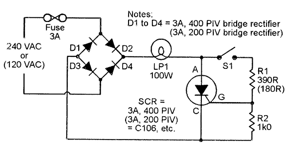
Figure 3 shows an SCR used in an AC power switching application; alternative component values are shown for use with 240V or (in parenthesis) 120V AC supplies. The AC power line signal is full-wave rectified via D1-D4 and applied to the SCR anode via lamp load LP1.
 |
 |
| FIGURE 3. Full-wave on-off SCR circuit with DC power load. |
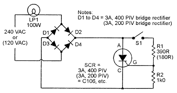
FIGURE 4. Full-wave on-off SCR circuit with AC power load. |
If S1 is open, the SCR and lamp are off. If S1 is closed, R1-R2 apply gate drive to the SCR, which turns on and self-latches just after the start of each half-cycle and then turns off again automatically at the end of the half-cycle as its forward current falls below the minimum holding value. This process repeats in each half-cycle, and the lamp thus operates at full power under this condition.
The SCR anode falls to about 1V when the SCR is on, so S1 and R1-R2 consume little mean power. Note that the lamp load is shown placed on the DC side of the bridge rectifier, and this circuit is thus shown for use with DC loads; it can be modified for use with AC loads by simply placing the load on the AC side of the bridge, as in Figure 4.
Note that SCRs can also be used, in various ways, to apply variable AC power to various types of load, but that these tasks are usually best carried out by TRIACs, as will be described in a future article; two special types of SCR variable AC power control circuits are, however, shown at the end of the present article.
Bell/buzzer alarm circuits
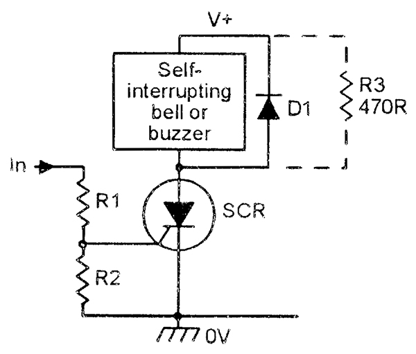 |
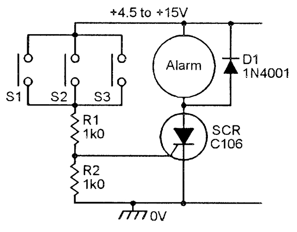
| FIGURE 5. Basic SCR alarm circuit. |
 |
| FIGURE 6. Multi-input non-latching alarm circuit. |
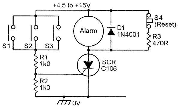 |
| FIGURE 7. Multi-input self-latching panic alarm. |
One useful application of the SCR is in DC-powered 'alarm' circuits that use self-interrupting loads such as bells or buzzers; these loads comprise a solenoid and a series switch, and give an action in which the solenoid first shoots forward via the closed switch, and in doing so, forces the switch to open, thus making the solenoid fall back and re-close the switch, thus restarting the action, and so on.
Figure 5 shows such an alarm circuit; it effectively gives a non-latching load-driving action, since the SCR unlatches automatically each time the load self-interrupts. The circuit can be made fully self-latching, if desired, by shunting the load with resistor R3, as shown, so that the SCR anode current does not fall below the SCR's minimum holding value as the load self-interrupts.
Figures 6 to 14 show a selection of alarm circuits of this type. All of these are designed around the inexpensive type C106 SCR, which can handle mean load currents up to 2.5 amps, needs a gate current of less than 200mA, and has a 'minimum holding current' value of less than 3mA. Note in all cases that the supply voltage should be about 1.5V greater than the normal operating voltage of the alarm device used, to compensate for voltage losses across the SCR, and that diode D1 is used to damp the alarm's back-EMFs.
Figure 6 shows a simple non-latching multi-input alarm, in which the alarm activates when any of the S1 to S3 push-button input switches are closed, but stops operating as soon as the switch is released.
Figure 7 shows the above circuit converted into a self-latching multi-input 'panic' alarm by wiring R3 plus normally-closed reset switch S4 in parallel with the alarm device. Once this circuit has latched, it can be unlatched again (reset) by briefly opening S4.
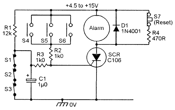
Figure 8 shows a simple burglar alarm system, complete with the 'panic' facility. The alarm can be activated by briefly opening any of the S1 to S3 'burglar alarm' switches (which can be reed-relays or microswitches that are activated by the action of opening doors or windows, etc.), or by briefly closing any of the 'panic' switches. C1 acts as a noise-suppressor that ensures that the alarm only activates if the S1 to S3 switches are held open for more than a millisecond or so, thus enhancing the circuit's reliability. The circuit consumes a typical standby current of 0.5mA (via R1) from a 6V supply.
 |
 |
| FIGURE 8. Simple burglar alarm system, with panic facility. |
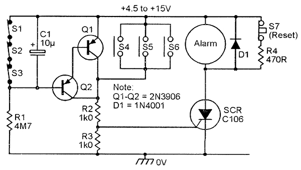
FIGURE 9. Improved burglar alarm circuit. |
The standby current of the burglar alarm circuit can be reduced to a mere 1.4mA (at 6V) by modifying it as shown in Figure 9, where Q1 and Q2 are connected as a Darlington common emitter amplifier that inverts and boosts the R1-derived 'burglar' signal and then passes it on to the gate of the SCR. Here, C1 is used as a time-delay component that ensures that the alarm only activates if the S1 to S3 switches are held open for more than a few seconds; the C1 value can be greatly reduced, if desired.
Water, light, and heat alarms
The basic SCR-driven alarm circuit can be used to indicate the presence of excess water, light, or temperature levels by driving the SCR gate via suitable sensing circuitry; Figures 10 to 14 show alarm circuits of this type.
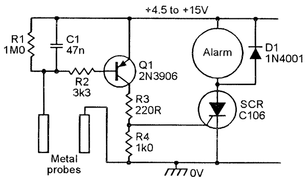
The Figure 10 'water-activated' alarm uses Q1 to activate the SCR when a resistance of less than about 220k appears across the two metal probes. Its operation as a water-activated alarm relies on the fact that the impurities in normal water (and many other liquids and vapors) make it act as a conductive medium with a moderately low electrical resistance, which thus causes the alarm to activate when water comes into contact with both probes simultaneously.
 |
 |
| FIGURE 10. Water-activated alarm. |
FIGURE 11. Light-activated alarm. |
C1 suppresses unwanted AC signal pick-up, and R2 limits Q1's base current to a safe value. By suitably adjusting the placing of the two metal probes, this circuit can be used to sound an alarm when water rises above a pre-set level in a bath, tank, or cistern, etc.
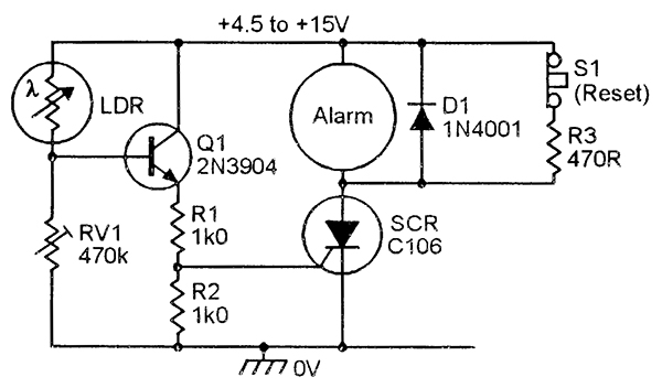
Figure 11 is a 'light-activated' circuit that can be used to sound an alarm when light enters a normally-dark area such as a drawer or wall safe, etc. The LDR and RV1 form a light-sensitive potential divider that has its output buffered via Q1 and fed to the SCR gate via R1; this output is low under dark conditions (LDR resistance is high), but goes high under bright conditions (LDR resistance is low), and thus drives the SCR and alarm on; the light-triggering point can be pre-set via RV1. Almost any small cadmium sulphide photocell can be used in the LDR position.
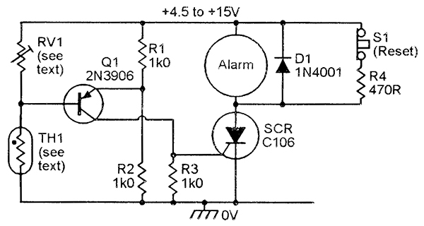
Temperature-activated alarms can be used to indicate either fire or overheat conditions, or frost or underheat conditions. Figures 12 to 14 show three such circuits; in each of these, TH1 can be any NTC thermistor that has a resistance in the range 1k0 to 20k at the required trigger temperature; pre-set pot RV1 needs a maximum resistance value roughly double that of TH1 under this trigger condition.
The Figure 12 over-temperature alarm uses R1-R2 and TH1-RV1 as a Wheatstone bridge in which R1-R2 generates a fixed half-supply 'reference' voltage and TH1-RV1 generates a temperature-sensitive 'variable’ voltage, and Q1 is used as a bridge balance detector and SCR gate driver. RV1 is adjusted so that the 'reference' and 'variable' voltages are equal at a temperature just below the required trigger value, and under this condition, Q1 base and emitter are at equal voltages and Q1 and the SCR are thus cut off.
 |
 |
| FIGURE 12. Simple over-temperature alarm. |
FIGURE 13. Simple frost or under-temperature alarm. |
When the TH1 temperature goes above this 'balance' value, the TH1-RV1 voltage falls below the 'reference' value, so Q1 becomes forward-biased and drives the SCR on, thus sounding the alarm. The precise trigger point can be pre-set via RV1.
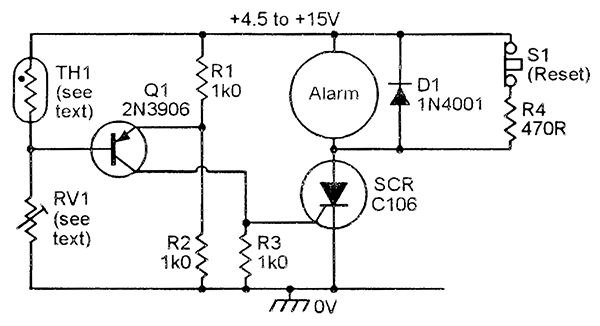
The circuit's action can be reversed, so that the alarm turns on when the temperature falls below a pre-set level, by simply transposing the TH1 and RV1 positions as shown in the frost or under-temperature alarm circuit of Figure 13.
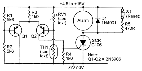 |
FIGURE 14. Precision over-temperature alarm.
|
Note in these two circuits that if TH1 and Q1 are not mounted in the same environment, the precise trigger points are subject to slight variation with changes in Q1 temperature, due to the temperature dependence of its base-emitter junction characteristics. These circuits are thus not suitable for use in precision applications, unless Q1 and TH1 operate at equal temperatures.
This snag can be overcome by using a two-transistor differential detector in place of Q1, as shown in the Figure 14 over-temperature alarm, which can be made to act as a precision under-temperature alarm by simply transposing RV1 and TH1.
Variable AC power control
All SCR circuits shown so far give an on/off form of power control. SCRs (and TRIACs) can be used to give variable power control in AC circuits in several ways. One of these is via the 'phase-delayed switching' technique of Figure 15, in which power is fed to the load via a self-latching solid-state power switch that can be triggered (via a variable phase-delay network and a trigger pulse generator) at any point in each power half-cycle, and automatically unlatches again at the end of each half-cycle. The diagram shows the load voltage waveforms that can be generated.
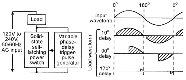 |
| FIGURE 15. Variable phase-delay-switching AC power controller with waveforms. |
Thus, if the power switch is triggered near the start of each half-cycle (with near 0° phase delay), the mean load voltage equals almost the full supply value, and the load consumes near-maximum power; if it is triggered near the end of each half-cycle (with near-180° phase delay), the mean load voltage is near-zero, and the load consumes minimal power; by varying the trigger signal's phase-delay between these extremes, the load's power feed can be varied between zero and maximum.
This form of variable power control is very efficient (typically 95%), and can (among other things) be used to control the speeds of many types of electric motor, including those of electric drills and model trains (see Figures 16 and 17).
A drill-speed controller
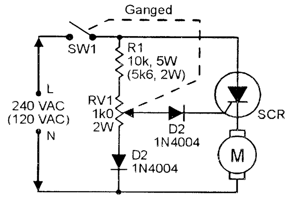 |
| FIGURE 16. Electric drill speed controller. |
Most electric drills are powered by series-wound 'universal' (AC/DC) electric motors. These motors generate a back-EMF that is proportional to the motor speed, and the motor's effective applied voltage thus equals the true applied voltage minus the back-EMF; this gives the motor a degree of speed self-regulation, since any increase in motor loading tends to reduce the speed and back-EMF, thereby increasing the effective applied voltage and causing the motor speed to rise towards its original value, and so on.
The speed of an electric drill can be varied electronically by using the 'phase-delayed switching' technique. Figure 16 shows a particularly effective yet simple variable speed-regulator circuit. This uses an SCR as the control element and feeds half-wave power to the motor (this causes a 20% reduction in maximum available speed/power), but in the off half-cycles, the back-EMF of the motor is sensed by the SCR and used to give automatic adjustment of the next gating pulse, to give automatic speed regulation.
The R1-RV1-D1 network provides only 90° of phase adjustment, so all motor pulses have minimum durations of 90° and provide very high torque. At low speeds, the circuit goes into a high-torque 'skip cycling' mode, in which power pulses are provided intermittently, to suit motor loading conditions.
Model-train speed controller
Figure 17 shows how the 'phase-delayed switching' technique can be used to make an excellent 12-volt model-train speed controller that enables speed to be varied smoothly from zero to maximum.
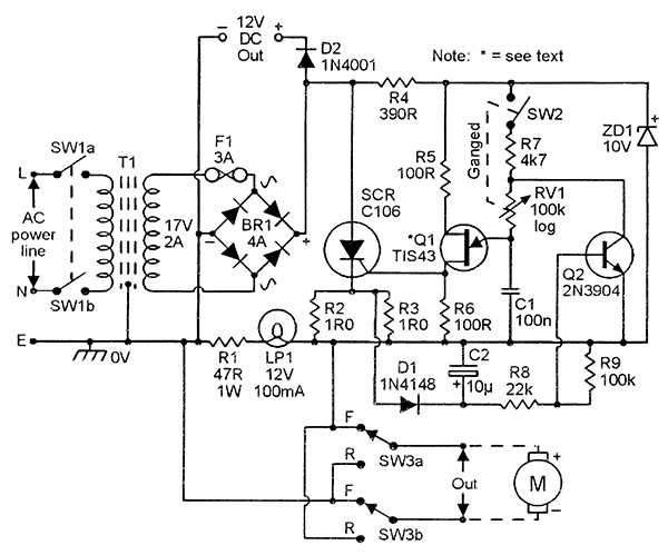 |
| FIGURE 17. Model train speed-controller circuit with automatic short-circuit protection. |
The maximum available output current is 1.5 amps, but the unit incorporates short-circuit sensing and protection circuitry that automatically limits the output current to a mean value of only 100mA if a short occurs on the track. The circuit operates as follows.
The circuit's power line voltage is stepped down via T1 and full-wave (bridge) rectified via BR1, to produce a raw (unsmoothed) DC supply that is fed to the model train (via the track rails) via the series-connected SCR and direction control switch SW3.
At the start of each raw DC half-cycle, the SCR is off, so DC voltage is applied (via R4 and ZD1) to unijunction transistor (UJT) Q1 and its associated C1-RV1 (etc.) timing circuitry, and C1 starts to charge up until eventually the UJT fires and triggers the SCR; as the SCR turns on, it saturates, removing power from Q1 (which thus resets) and feeding the rest of the power half-cycle to the model train via R2//R3 (= R2 and R3 in parallel) and SW3.
This timing/switching process repeats in each raw DC half-cycle (i.e., at twice the power line frequency), giving a classic phase-triggered power control action that enables the train speed to be varied over a wide range via RV1.
Note that the circuit's output current passes through R2/R3, which generate a proportional output voltage that is peak-detected and stored via D1-C2 and fed to Q2 base via R8-R9.
The overall action is such that, because of the voltage storing action of C2, Q2 turns on and disables the UJT's timing network (thus preventing the SCR from firing) for several half-cycles if the peak output current exceeds 1.5 amps.
Thus, if a short occurs across the track, the half-cycle output current is limited to a peak value of a few amps by the circuit's internal resistance, but the protection circuitry ensures that the SCR fires only once in (say) every 15 half-cycles, thus limiting the mean output current to a mere 100mA or so.
Note that the UJT shown here is an obsolete TIS43 type, and that in practice any TIS43 or 2N2646 near-equivalent UJT can be used in its place.
Optocoupled SCRs
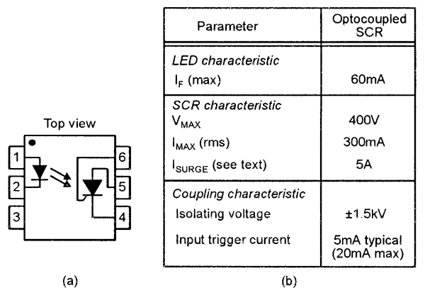 |
| FIGURE 18. Typical outline (a) and characteristics (b) of an optocoupled SCR. |
 |
| FIGURE 19. High-power control via an optocoupled SCR slave. |
SCRs are semiconductor power switching devices that (like transistors) are inherently photosensitive. An optocoupled SCR is simply an SCR and a LED mounted in a single package and configured so that the SCR's gate current is controlled by the LED's optical output, thus enabling the SCR to be controlled by a remote input current that is electrically fully isolated from the SCR's output (load) circuitry.
Figure 18(a) shows the typical outline of an optocoupled SCR that is mounted in a six-pin DIL package, and Figure 18(b) lists the typical parameter values of such a device, which has a mean output load current rating of only 300mA but has a surge current rating of 5A at a pulse width of 100mS and a duty cycle of 1%.
Optocoupled SCRs are very easy to use; the input LED is driven in the way of a normal LED, and the SCR is used like a normal low-power SCR.
The most important application of the optocoupled SCR is a 'slave' device that controls the gate current of a high-power SCR, which can activate a load of any desired power rating. Figure 19 shows an example of this type of application. NV