INTRODUCTION
Security circuits that react to temperature, voltage, current, or resistance have many practical applications in the home and in commerce and industry.
Temperature-sensitive circuits can be used to automatically activate alarms or safety devices when one or more monitored temperatures goes above or below a preset level, or when two temperatures differ by more than a preset amount.
Such circuits can be used to give warning of fire, frost, excessive boiler temperature, the failure of a heating system, or over-heating of a piece of machinery or a liquid, etc., and may use thermostats, thermistors, or various types of solid-state devices as their temperature-sensing elements.
The first half of this article presents a selection of practical temperature-sensitive security circuits.
Circuits that react to an input voltage, current, or resistance also have many practical applications, since these inputs may, in fact, be derived from the output of a transducer that monitors a parameter such as motor speed, liquid flow rate or pressure, or rate of linear movement, etc.
The second half of this article presents a selection of practical voltage-, current-, or resistance-sensitive security circuits.
Note that most practical circuits shown here are designed to activate a relay under the ‘alarm’ condition but that, in most cases, this relay can be replaced by a ready-built 12V piezo-siren module if required.
Temperature-Sensitive Security Circuits
THERMOSTAT FIRE-ALARM CIRCUITS
One of the simplest types of temperature-sensitive circuit is the thermostat-activated fire alarm. Figure 1 shows the practical circuit of a relay-aided non-latching alarm of this type. Here, any desired number of n.o. thermostats are wired in parallel and then connected in series with the coil of a relay, and one set of the relay’s n.o. contacts are wired in series with the alarm bell so that the bell operates if the relay turns on.
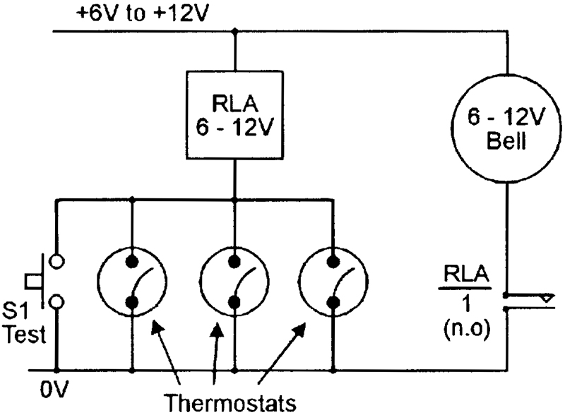
FIGURE 1. Simple relay-aided non-latching fire alarm.
Normally, the thermostats are all open, so the relay and alarm bell are off. Under this condition, the circuit consumes zero standby current. At ‘overheat’ temperatures, on the other hand, one or more of the thermostats closes, and thus turns on the relay and thence the alarm bell. Note that push-button switch S1 is wired in parallel with the thermostats, enabling the circuit to be functionally tested by operating the push-button.
The basic Figure 1 circuit gives a non-latching form of operation. If required, the circuit can be made self-latching by wiring a spare set of n.o. relay contacts in parallel with the thermostats, as shown in Figure 2. Note that n.c. push-button switch S2 is wired in series with these relay contacts, so that the circuit can be reset or unlatched by momentarily operating S2.
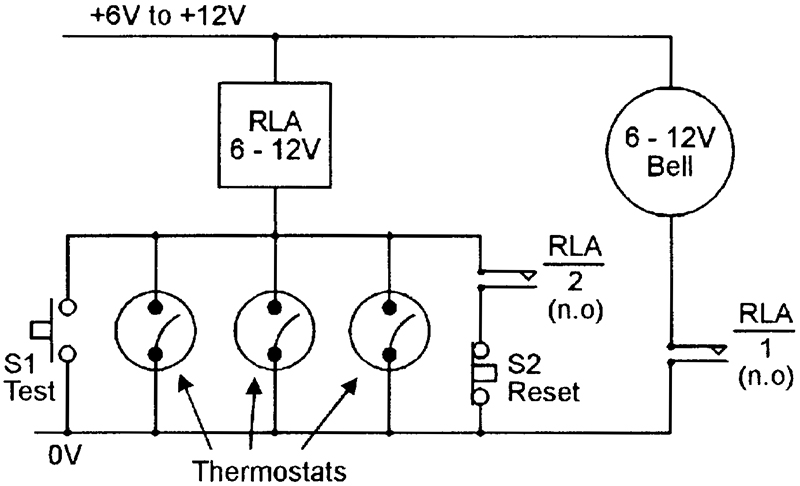
FIGURE 2. Simple relay-aided self-latching fire alarm.
The thermostats used in the above two circuits must be n.o. types that close when the temperature exceeds a preset limit. When the thermostats are located in normal living areas, they should be set at a temperature of roughly 60°C (140°F), but when they are located in unusually warm places — such as furnace rooms or attics — they should be set at about 90°C (194°F).
OVER- and UNDER-TEMPERATURE SECURITY CIRCUITS
Most over-temperature (and under-temperature) security circuits activate a relay or an alarm unit when a monitored temperature rises above (or falls below) a preset level, which may range from well below the freezing point of water to well above the boiling point of water. Precision circuits of this type usually use one or more thermistors or solid-state devices as their temperature-sensing elements.
Two useful over-temperature security circuits (and two under-temperature circuits) are de-scribed in this section. The first two circuits use an inexpensive n.t.c. (negative temperature coefficient) thermistor as a temperature-sensing element.
This device acts as a temperature-sensitive resistor that presents a high resistance at low temperatures and a low resistance at high temperatures.
The thermistor circuits described in this and the following sections of this article have all been designed to work with thermistors that present a nominal resistance of 5K0 at the desired operating temperature; all of these circuits will, however, in fact, work well with any n.t.c. thermistors that present a resistance in the range 1K0 to 20K at the required ‘trip’ temperature.
Figure 3 shows the practical circuit of a simple but very sensitive over-temperature switch that has a relay output.
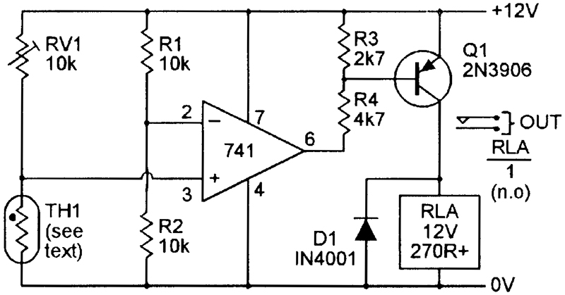
FIGURE 3. Relay-output precision over-temperature switch.
Here, the thermistor (TH1) and RV1-R1-R2 are wired in the form of a simple Wheatstone bridge in which R1-R2 generate a fixed half-supply ‘reference’ voltage and TH1-RV1 generate a ‘variable’ output voltage that is inversely proportional to the TH1 temperature and is trimmed (via RV1) so that it almost equals the R1-R2 reference value at the required ‘trip’ temperature.
These two voltages are fed to the input of the type 741 op-amp which is used — in conjunction with transistor Q1 — as the bridge’s balance detector and relay driver. The 741 op-amp is used in the open-loop mode in this circuit, and its action is such that its pin 6 output is driven low (to negative saturation) if its pin 3 (non-inverting) input is more than a few millivolts negative to the pin 2 (inverting) input, and is driven high (to positive saturation) if pin 3 is significantly positive to pin 2.
Suppose, then, that the bridge is adjusted so that it is close to balance at the desired ‘trip’ temperature. When the temperature falls below this value, the TH1 resistance increases, so the 741’s pin 3 voltage rises above that of pin 2, and the pin 6 output voltage thus goes to positive saturation and consequently applies no base drive to Q1; Q1 and the relay are off under this condition.
When the temperature rises above the ‘trip’ value, however, the TH1 resistance decreases and the 741’s pin 3 voltage falls below that of pin 2, and the pin 6 output voltage thus goes to negative saturation and applies heavy base drive to Q1; Q1 and the relay are driven on under this condition.
Thus, the relay goes on when the temperature rises above the preset level, and turns off when the temperature falls below the preset level.
Important points to note about the Figure 3 circuit are that, because it uses the bridge sensing configuration, its accuracy is independent of variations in supply voltage, and that the circuit can respond to TH1 resistance changes of less than 0.1 percent, i.e., to temperature changes of a fraction of a degree.
Figure 4 shows the above circuit converted into a precision under-temperature switch by simply transposing the op-amp’s pin 2 and pin 3 input connections; alternatively, the Figure 3 circuit can be made to give under-temperature operation by simply transposing the R1 and TH1 positions, or by redesigning the Q1 output stage so that it uses an npn transistor in place of the pnp device.
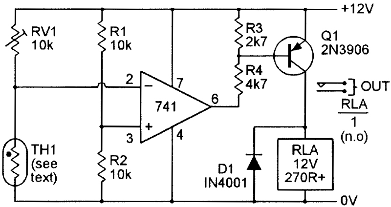
FIGURE 4. Relay-output precision under-temperature switch.
The Figure 3 and 4 circuits use a thermistor with a nominal trip-level resistance value of 5K0 as its temperature-sensing element, and this thermistor dissipates several milliwatts of power under actual working conditions.
In some special applications, this power dissipation may cause enough self-heating of the thermistor to upset its thermal sensing capability. In such cases, an alternative type of temperature-sensing device — such as an ordinary silicon diode — may have to be used.
Ordinary silicon diodes have temperature-dependent forward volt-drop characteristics, and can thus be used as temperature-sensing elements. Typically, a silicon diode gives a forward volt drop of about 600mV at a current of 1mA. If this current is held constant, the volt drop changes by about -2mV for each degree Centigrade increase in diode temperature.
All silicon diodes have similar thermal characteristics. Since the power dissipation of the diode is a mere 0.6mW under the above condition, negligible self-heating takes place in the device, which can thus be used as an accurate temperature sensor.
Figure 5 shows how general-purpose silicon diode D1 can be used as a thermal sensing element in an op-amp over-temperature relay-switch circuit. Here, zener diode ZD1 is wired in series with R1 so that a constant 5.6V is developed across the two potential dividers formed by R2-RV1 and R3-D1, and a near-constant current thus flows in each of these dividers.
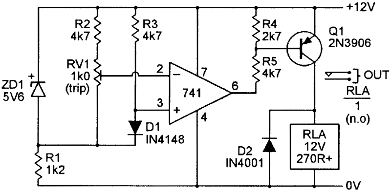
FIGURE 5. Relay-output over-temperature switch using silicon diode temperature-sensing element.
A constant reference voltage is thus developed between the R1-RV1 junction and pin 2 of the op-amp, and a temperature-dependent voltage with a coefficient of -2mV/°C is developed between the R1-RV1 junction and pin 3 of the op-amp. Thus, a differential voltage with a coefficient of -2mV/°C appears between pins 2 and 3 of the op-amp.
In practice, this circuit is set up by simply raising the temperature of D1 to the required over-temperature trip level, and then slowly trimming RV1 so that the relay just turns on. Under this condition, a differential temperature of about 1mV appears between pins 2 and 3 of the op-amp, the pin 3 voltage being below that of pin 2, and Q1 and the relay are driven on.
When the temperature falls below the trip level, the pin 3 voltage rises above that of pin 2 by about -2mV/°C change in temperature, so Q1 and the relay turn off. The circuit has a typical sensitivity of about 0.5°C, and can be used as an over-temperature switch at temperatures ranging from sub-zero to above the boiling point of water.
Figure 6 shows how the operation of the Figure 5 circuit can be reversed, so that it functions as an under-temperature switch, by simply transposing the pin 2 and pin 3 connections of the op-amp.
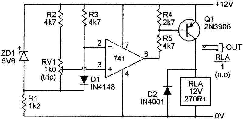
FIGURE 6. Relay-output under-temperature switch using silicon diode temperature-sensing element.
MISCELLANEOUS TEMPERATURE SWITCHES
Each temperature-sensitive circuit shown so far in this article activates when a monitored temperature goes either above or below a preset level. The present section shows three other types of temperature-sensitive security circuit.
Two of these circuits activate relays if the temperature deviates from a preset level by more than a preset amount, and the third activates a relay if two monitored temperatures differ by more than a preset amount. In all cases, the relay(s) can be used to operate any type of electrical alarm or slave device.
Figures 7 and 8 show the circuits of a pair of temperature-deviation switches, which activate if the temperature deviates from a preset level by more than a preset amount. The Figure 7 circuit has independent over-temperature and under-temperature relay outputs, while the Figure 8 circuit has a single relay output that activates if the temperature goes above or below preset levels.
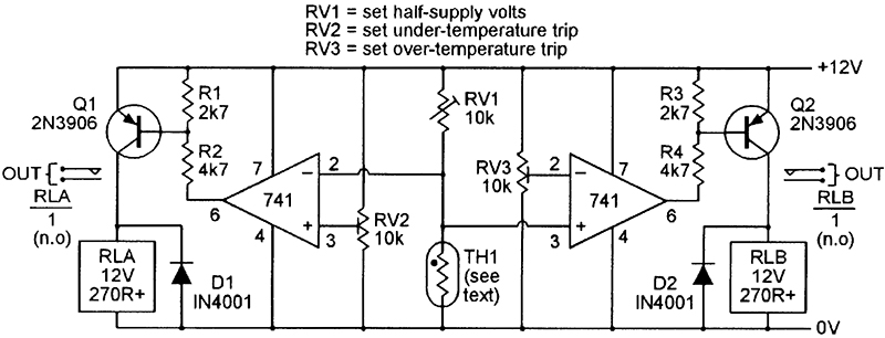
FIGURE 7. Temperature-deviation switch with independent over/under-temperature relay outputs.
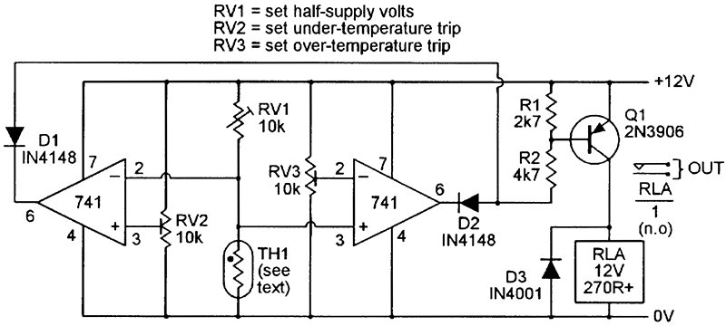
FIGURE 8. Temperature-deviation switch with single relay output.
Both of these circuits are made by combining the basic over-temperature and under-temperature circuits of Figures 3 and 4. The right (over-temperature) half of each circuit is based on that of Figure 3, and the left (under-temperature) half is based on that of Figure 4.
Both halves of the circuit share a common RV1-TH1 temperature-sensing network, but the under-temperature and over-temperature switching levels of the circuits are independently adjustable.
Each of the two op-amp outputs of the Figure 7 circuit are taken to independent transistor-relay output stages, while the two op-amp outputs of the Figure 8 circuit are taken to a single transistor-relay output stage via the D1-D2 gate network. The procedure for setting up the two circuits is as follows.
First, set RV2 and RV3 to mid-travel, then, with TH1 at its normal or mid-band temperature, adjust RV1 so that half-supply volts are developed across TH1. Now fully rotate the RV2 slider towards the positive supply line, rotate the RV3 slider towards the zero volts line, and check that no ‘trip’ condition is indicated (relays off).
Next, reduce TH1’s temperature to the required under-temperature trip value and adjust RV2 so that the appropriate relay goes on to indicate the ‘trip’ condition. Now increase the TH1 temperature slightly and check that the relay turns off.
Finally, raise the TH1 temperature to the required over-temperature trip level and adjust RV3 so that the appropriate relay turns on to indicate the ‘trip’ condition. The circuits are then ready for use.
Figure 9 shows the circuit of a differential-temperature switch that activates a relay if two monitored temperatures differ by more than a preset amount. The circuit uses a pair of silicon diodes as temperature-sensing elements, and activates the relay only when the temperature of D1 is more than a preset amount greater than that of D2, and is not influenced by the absolute temperatures of the two diodes.
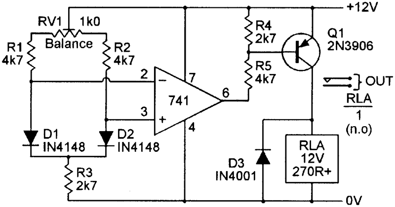
FIGURE 9. Differential-temperature switch with relay output.
In this circuit, general-purpose silicon diodes D1 and D2 are used as temperature-sensing elements. A standing current is passed through D1 from the positive supply rail via RV1-R1 and R3, and a similar current is passed through D2 via RV1-R2 and R3. The relative values of these currents can be adjusted over a limited range via RV1, thus enabling the forward volt drops of the diodes to be equalized, so that they give zero differential output when they are both at the same temperature.
Suppose then that the diode voltages have been equalized in this way, so that zero voltage differential exists between them. If now the temperatures of both diodes are raised by 10°C, the forward voltages of both diodes will fall by 20mV, and zero differential will still exist between them. The circuit is thus not influenced by identical changes in the temperatures of D1 and D2.
Suppose next that the temperature of D2 falls 1°C below that of D1; in this case, the D2 voltage will rise 2mV above that of D1, so the op-amp’s pin 3 voltage goes positive to that of pin 2, thus driving the op-amp output to positive saturation and holding Q1 and the relay off.
Finally, suppose that the temperature of D2 rises 1°C above that of D1; in this case, the D2 voltage will fall 2mV below that of D1, so the op-amp output goes into negative saturation and drives Q1 and the relay on. Thus, the relay turns on only when the temperature of D2 is above that of D1. The circuit has a typical sensitivity of 0.5°C.
The above explanation assumes that RV1 is adjusted so that the D1 and D2 voltages are equalized when the two diodes are at the same temperature, so that the relay goes on when the D2 temperature rises a fraction of a degree above that of D1. In practice, RV1 is usually adjusted so that the standing bias voltage of D2 is some millivolts greater than that of D1 at normal temperatures, in which case, the relay will not turn on until the temperature of D2 rises some where above that of D1.
The magnitude of this differential temperature trip level is fully variable from zero to about 10°C via RV1, so the circuit is quite versatile. The circuit can be set up by raising the temperature of D2 the required amount above that of D1, and then trimming RV1 so that the relay just turns on under this condition.
DC VOLTAGE-ACTIVATED CIRCUITS
Figure 10 shows the practical circuit of a precision DC over-voltage switch that activates only when the input voltage is greater than some pre-set value in excess of at least 5V. Here, the op-amp is used in the open-loop mode as a DC voltage comparator, with a Zener-derived 5V reference applied to the op-amp’s non-inverting pin 3 input, and with the test voltage applied between the pin 2 inverting input and ground.
The circuit action is such that the op-amp output is positively saturated, and Q1 and the relay are off, when the pin 2 test voltage is fractionally less than the pin 3 5V reference value, and Q1 and the relay go on when the test voltage is greater than the 5V reference value.
Note in Figure 10 that Rx is wired in series between the input test voltage and the 10K (R1) impedance of the inverting input of the op-amp, and enables the circuit to be ‘ranged’ so that it triggers at any required voltage in excess of the 5V reference value. The Rx value for any required trigger voltage is determined on the basis of (2K0 x V) - 10K. Thus, for 50V triggering, Rx = (50 x 2K0) - 10K = 90K. For 5V triggering, Rx must have a value of zero ohms.
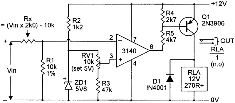
FIGURE 10. Precision DC over-voltage switch, covering 5V upwards.
The Figure 10 circuit is very sensitive and exhibits negligible back-lash. Triggering accuracies of 0.5 percent can easily be achieved. For maximum accuracy, either the power supply or the zener reference voltage of the circuit should be fully stabilized.
The Figure 10 circuit can be made to function as a precision under-voltage switch, which turns on when the input voltage falls below a preset level, by simply transposing the inverting and non-inverting input pin connections of the op-amp, as shown in Figure 11.
FIGURE 11. Precision DC under-voltage switch, covering 5V upwards.
This circuit also shows how the zener reference supply can be stabilized for high-precision operation. Note in both of these circuits that, once 5V has been accurately set via RV1, the final triggering accuracy is determined solely by the accuracies of Rx and R1. In high-precision applications, therefore, these resistors must be stable high-precision types.
Figure 12 shows how the Figure 10 circuit can be modified for use as an over-voltage switch covering the range 10mV to 5V. In this case, the input voltage is connected directly to the op-amp’s inverting input terminal, and a variable reference voltage is applied to its non-inverting input terminal, and is adjusted to give the same value as that of the required trigger voltage.
FIGURE 12. Dual-supply precision DC over-voltage switch, covering 10mV to 5V.
The circuit action can be reversed, so that the design acts as an under-voltage switch, by transposing the input pin connections of the op-amp. Note that the Figure 12 circuit uses two sets of supply lines (+9V and -3V), to ensure proper biasing of the op-amp.
Figure 13 shows how the Figure 12 circuit can be adapted for operation from a single set of supply lines.
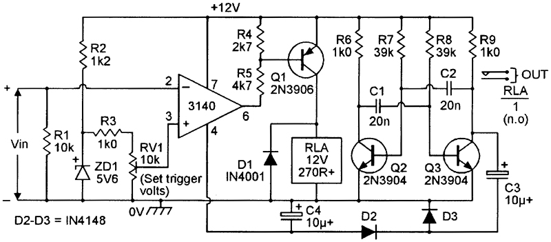
FIGURE 13. Single-supply precision DC over-voltage switch, covering 10mV to 5V.
Here, Q2 and Q3 are wired as an astable multivibrator or squarewave generator, and the output of this generator is used to provide a negative supply rail for the op-amp via the voltage-converting and smoothing D2-D3 and C3-C4 network, which actually gives a negative output of about 9V when unloaded, but this output falls to only 3 to 5 volts when it is loaded by connecting it to the pin 4 ‘negative supply’ terminal of the 3140 op-amp.
Finally, Figure 14 shows the circuit of a DC over-voltage switch that covers the range 10mV to 5V and uses a single floating supply. Here, the op-amp is again used as a DC voltage comparator, but its positive supply rail is set at 6.8V via the floating supply and zener diode ZD1, and its negative rail is set at -5.2V via the ZD1 and R2 combination.
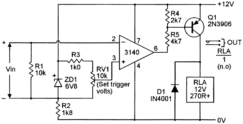
FIGURE 14. Single-supply DC over-voltage switch, covering 10mV to 5V.
The monitored input voltage is fed to the pin 2 inverting input of the op-amp, and the zener-derived reference voltage is fed to the pin 3 non-inverting input of the op-amp via potential divider R3-RV1.
This reference voltage can be varied between roughly 10mV and 5V, and this is therefore the voltage range covered by this over-voltage switch.
AC VOLTAGE-ACTIVATED CIRCUITS
The five voltage-activated switches shown in Figures 10 to 14 are all designed for DC activation only. All of these circuits can be modified for AC activation by interposing suitable rectifier/smoothing networks or AC/DC converters between their input terminals and the actual AC input signals, so that the AC signals are converted to DC before being applied to the switching circuits.
Figure 15 shows the practical circuit of a precision AC over-voltage switch that is designed to work with sinewave signals in excess of 2.5V RMS. Here, the AC signal is converted to DC via the voltage-converting and smoothing network formed by Rx-C1-D1-D2-C2-R1, and the resulting DC voltage is applied to the pin 2 inverting input of the op-amp via R2.
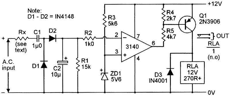
FIGURE 15. Precision AC over-voltage switch, covering 2.5V upwards.
A zener-derived 5.6V reference voltage is applied to the op-amp’s non-inverting input terminal, and the circuit action is such that — when Rx has a value of zero — Q1 and the relay turn on when the DC voltage on pin 2 exceeds 5.6V.It is important to note in Figure 15 that the voltage-converting and smoothing network actually gives a DC output voltage that is somewhat less than the peak voltage value of a symmetrical sinewave input signal. This type of network cannot be used to measure the RMS values of non-symmetrical or pulse-type waveforms.
Also note that the action of the Figure 15 circuit can be reversed, so that it acts as an under-voltage switch, by simply transposing the input terminal connections of the op-amp, as shown in Figure 16.
FIGURE 16. Precision AC under-voltage switch, covering 2.5V upwards.
The Figures 15 and 16 circuits both have a basic input impedance — with Rx reduced to zero ohms — of 15K (= R1) and, under this condition, a sinewave of about 2.5V RMS is needed to activate the switch.
Consequently, when Rx is given a finite value, it acts as a potential divider with the 15K input impedance, and enables the circuits to be triggered at any required AC input level in excess of 2.5V.
The Rx value is chosen on the basis of roughly (6K0 x V) - 15K. Thus, if a circuit is to be activated at an input signal level of 10V RMS, Rx must have a value of about 45K.
If required, the effective sensitivities of the Figure 15 and 16 circuits can be increased, so that they trigger at sinewave input levels substantially less than 2.5V RMS, by simply feeding the AC input signals to the inputs of the switching circuits via fixed-gain transistor or op-amp preamplifiers. Alternatively, the simple AC/DC converters used in these circuits can be replaced by high-gain precision types.
CURRENT-ACTIVATED CIRCUITS
Each of the five DC voltage switch circuits of Figures 10 to 14 can be used as a DC (power-level) current switch by simply feeding the monitored DC current to the input of the voltage switch via a current-to-voltage converter. A suitable converter circuit is shown in Figure 17.
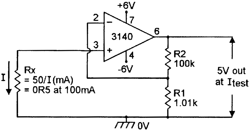
FIGURE 17. DC current-to-voltage converter.
In Figure 17, the op-amp is wired as a non-inverting x100 voltage amplifier, with its gain controlled by the ratios of R1 and R2. The test current is passed through input resistor Rx, which has its value chosen so that 50mV is developed across it at the required trigger current, thus giving 5V output from the op-amp under this condition; this 5V output is used to trigger the external voltage switch.
The circuit’s Rx value is selected on the basis of
Rx = 50/I(mA)
where I(mA) is the desired trigger current in milliamps. Thus, Rx needs a value of 0R5 at a trigger current of 100mA, or 0.05 ohms at a trigger level of 1A, and so on.
Note that the Figure 17 type of converter circuit can also function as an AC current-to-voltage converter, and can be used to make an AC current switch by connecting its output to the input of a suitable AC voltage switch circuit.
If required, an op-amp circuit can be built specifically for use as a DC over-current switch by using the circuit shown in Figure 18. Here, Rx is again used to develop 50mV at the desired test current level, and this voltage is applied to the inverting pin of the op-amp.
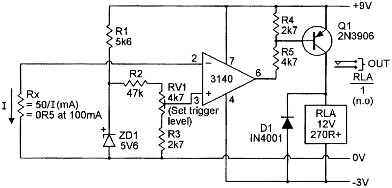
FIGURE 18. DC over-current switch.
A zener-derived reference of approximately 50mV is applied to the non-inverting input terminal of the op-amp; this reference voltage can be adjusted over a limited range via RV1, thus providing a limited control of the circuit’s sensitivity.
Thus, the Figure 18 switch circuit’s relay turns on when the current-derived input voltage exceeds the 50mV reference voltage. The circuit’s action can be reversed, so that it acts as an under-current switch, by simply transposing the op-amp’s two input terminal connections. In either case, the value of monitor resistor Rx is chosen on the basis of
Rx = 50/I(mA)
where I(mA) is the desired trigger current in milliamps. Thus, Rx needs a value of 0R5 at a trigger current of 100mA, or 0.05 ohms at a trigger level of 1A, and so on.
RESISTANCE-ACTIVATED CIRCUITS
Figure 19 shows the practical circuit of a precision under-resistance switch that turns on when the value of a monitored resistance falls below a specific value.
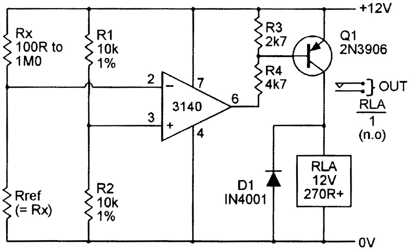
FIGURE 19. Precision under-resistance switch.
Here, the op-amp is again used as a voltage comparator, with its output fed to the coil of relay RLA via transistor Q1 but, in this case, the voltage on the op-amp’s non-inverting input pin is set at half-supply volts via potential divider R1-R2, and the voltage on the inverting input pin is determined by the ratios of Rx and Rref.
In effect, these four resistors are wired as a Wheatstone bridge, and the circuit action is such that the relay turns on when the value of Rx falls below that of reference resistor Rref, i.e., when the bridge goes out of balance in such a way that the voltage on the op-amp’s inverting input terminal rises above that on its non-inverting input terminal.
In this circuit, Rref must have the same value of the desired Rx ‘trigger’ resistance value, which can have any value in the range 100R to 1M0.
The minimum usable resistance value is dictated by the current-driving capability of the circuit’s power supply (and the power dissipation limits of Rref and Rx), and the maximum value is restricted by the shunting effect that the op-amp’s input impedance and leakage impedance has in the effective value of Rref.
The accuracy of the above circuit is (within sensible limits) quite independent of variations in power-supply voltage, and the ‘switch’ circuit is capable of responding to changes of less than 0.1 percent in the value of Rx.
The actual accuracy of the circuit is determined by the precisions of R1-R2 and Rref, and in worst-case terms is equal to the sum of the tolerances of these three resistors, i.e., it equals ±3% if ±1% percent resistors are used.
The action of the above circuit can be reversed, so that it acts as a precision over-resistance switch, by simply transposing the input pin connections of the op-amp, as shown in Figure 20.
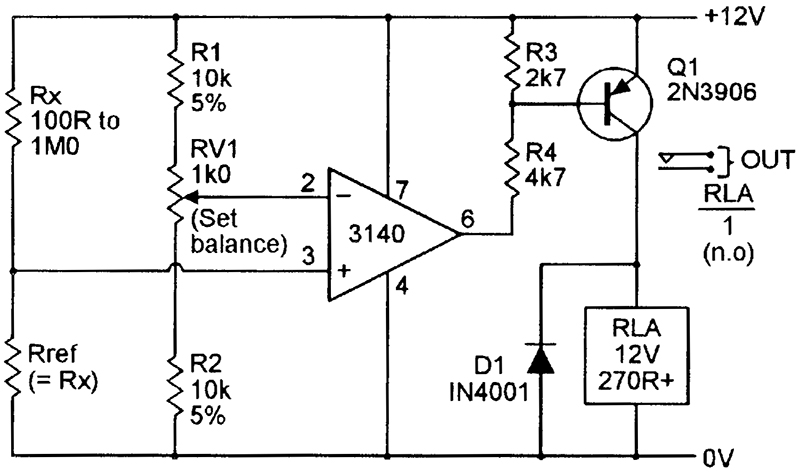
FIGURE 20. Precision over-resistance switch.
This circuit also shows how the basic accuracies of both designs can be improved by adding an RV1 ‘set balance’ control to the R1-R2 potential divider chain.
This control enables the bridge to be very precisely balanced (even when using ±5% R1-R2 components) so that the circuit ‘switches’ when the value of Rx varies from the marked value of Rref by only ±0.1% or so.
In this case, the true accuracy of the circuit is equal to the tolerance of Rref +0.1%. NV