Frequency Synthesizers
Part 1 of this two-part article introduced the topic of signal generators. This time, we will look at the frequency synthesizer. A synthesizer architecture is shown in Figure 1. This type of signal generator is more modern than the old-fashioned type, and is capable of producing very accurate, high-quality signals.
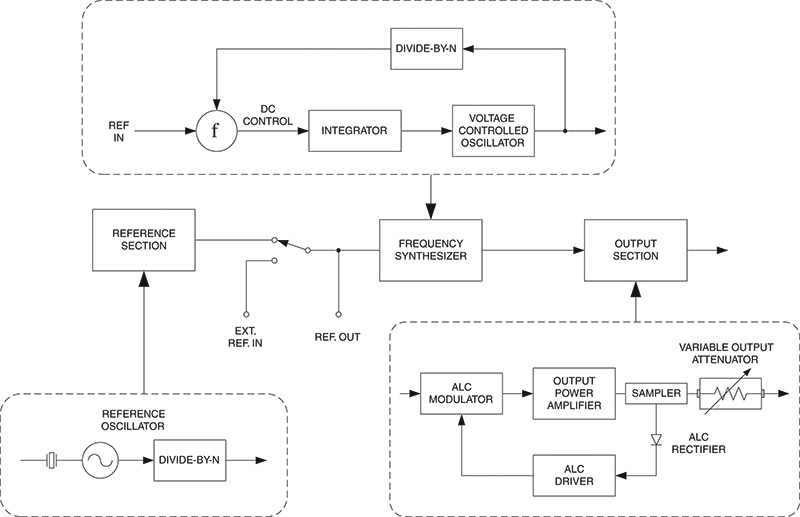
FIGURE 1.
There are three main sections to this signal source: Reference Section, Frequency Synthesizer, and Output Section. In Figure 1, each section is broken down into further components for sake of easy analysis.
Reference Section
The Reference Section is at the very core of the signal generation process. It is an accurate, stable, fixed-frequency source such as a crystal oscillator. The frequency of the reference section must be precisely adjustable over a small range so that it can be compared to a higher order standard, such as a Cesium-beam oscillator or WWVB comparator receiver, for purposes of calibration.
Because it controls the frequency synthesizer, the stability of the reference section determines the overall stability of the signal generator. The stability of ordinary crystal oscillators is reasonably good for many purposes, but not for use in the reference section of a signal source. For that purpose, either Temperature Compensated Crystal Oscillators (TCXO) or Oven Controlled Crystal Oscillators (OCXO) are used for the reference section. The TCXO will typically exhibit crystal aging of better then ±2 ppm/year, and a temperature aging of ±1 ppm/year. The OCXO is capable of 0.1 ppm/year for aging and 0.01 ppm/year for temperature.
The crystal oscillator is usually operated at a frequency such as 5 MHz, but lower frequencies are often needed. To generate these lower frequencies, a divide-by-N digital counter is provided. This circuit will divide the output frequency by some integer — N — to produce a much lower reference frequency.
Many signal generators provide REF. OUT and EXT. REF. IN capability (these connections are often located on the rear panel of signal generators, so may be overlooked). The REF. OUT connector provides the reference signal to other instruments, or can be used for calibration purposes. The EXT. REF. IN allows the use of an external reference source in place of the internal reference section. This is done sometimes to lock up two signal generators that must work together, or to substitute a much more accurate reference such as a Cesium-beam clock.
Frequency Synthesizer Section
The actual signal is produced in the frequency synthesizer section. It is generated by a voltage-controlled oscillator (VCO) whose output is compared to the reference signal. Voltage variable capacitance diodes (“varactors”) can be used for the VCO, as can surface acoustical wave (SAW) oscillators (which are used at higher frequencies and in the microwave bands).
The frequency of the VCO is set by a DC control voltage applied to its tuning input line. This control voltage is generated by integrating the output of a phase detector or phase comparator that receives the reference frequency and a divide-by-N version of the VCO frequency as inputs. When the two frequencies are equal, then the output of the phase detector is zero, so the VCO tuning voltage is at some quiescent value.
But, if the frequency of the VCO drifts, the phase detector output becomes non-zero. The integrator output ramps up in the direction that will cancel the frequency drift of the VCO. The VCO frequency is continuously held in check by corrections from the integrated output of the phase detector. This type of circuit is called a phase-locked loop (PLL).
Suppose, for example, a signal source has a reference of 5 MHz, and it is divided by 20 to produce a 250 KHz reference. If the frequency synthesizer divide-by-N stage is set for, say, N = 511, then the VCO output frequency will be 0.25 MHz x 511 = 127.75 MHz. Band switching, operating frequency, and frequency resolution are controlled by manipulating the reference frequency divide-by-N and VCO divide-by-N settings. In some cases, the frequency is entered by keypad, and this tells the signal generator how to set these values. Alternatively, “tunable” signal generators may have a digital encoder shaft connected to a front panel control.
Noise Floor
The noise component of the output signal is composed of thermal noise and phase noise. Of these two, the phase noise tends to dominate the performance of the signal source. Both the Reference Oscillator and VCO phase noise contributes to the overall output phase noise. There is a 20 LOG(N) degradation of the phase noise performance of the signal source because of the divide-by-N nature of the PLL. Fortunately, the bandwidth of the PLL tends to limit the contribution of the VCO phase noise to the overall phase noise performance.
Output Section
The output section performs three basic functions: It boosts power output to a specified maximum level; it provides precision control over the actual output level; and keeps the output level constant as frequency is changed.
The power amplifier is a wideband amplifier that produces an output level of some value in excess of the required maximum output level (e.g., +13 dBm). A calibrated precision attenuator can then be used to set the actual output level to any lower value required (e.g., -136 dBm to +13 dBm).
The accuracy of the output power setting is dependent on keeping the RF power applied to the attenuator input constant, despite the fact that oscillators (including VCOs) tend to exhibit output signal amplitude changes as frequency is changed. In older manual signal sources, there was a zero center RF voltmeter at the input of the attenuator, and the output coarse attenuator level could be manually set to the zero line, making the calibration of the fine attenuator meaningful. Modern signal sources, however, use an automatic level control (ALC) circuit to accomplish this job.
Automatic Level Control (ALC)
The ALC modulator is essentially an amplitude modulator that is controlled by a DC voltage developed by rectifying and filtering a sample of the RF output level. The ALC driver compares the actual output level with a preset value, and adjusts the control signal to the ALC modulator in a direction that cancels the error.
Modulators
A signal generator is said to differ from a signal source in that it will provide modulation of the CW signal. Although I believe that is a distinction without a practical difference, it is nonetheless a commonly held usage.
Amplitude Modulation (AM)
Amplitude modulation conveys intelligence over a radio carrier by means of varying the amplitude in accordance with the applied audio. The sinewave RF carrier is described by a(t) = Ac Sin(2 π fc t), where a(t) is the instantaneous amplitude, Ac is the peak amplifier, fc is the carrier frequency and t is time. When another signal is used to vary the amplitude of the carrier, amplitude modulation (AM) results:

where
µ is the depth of modulation fm is the modulating frequency (all other terms previously defined)
You will see the terms linear AM and logarithmic AM. The former is used when the depth of modulation is expressed as a percentage, and the latter when it is expressed in decibels (dB). Figure 2 shows the block diagram of the output section of a signal generator that offers amplitude modulation. The depth of modulation for most signal generators is adjustable over at least 0 to 30 percent, while some offer 100 percent AM.
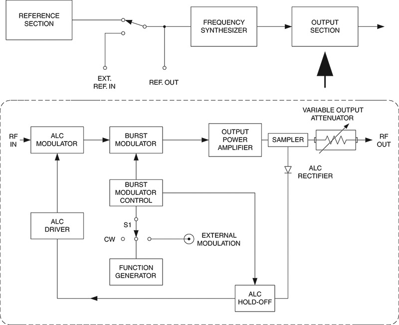
FIGURE 2.
The amplitude modulator is called a burst modulator in some signal generators, and is placed between the ALC modulator and the output power amplifier stage. The input signal used to modulate the RF carrier can be derived from an external source, or provided by an internal function generator that produces at least sinewaves. The function generator might also produce square waves, sawtooth waves, triangle waves, or pulses, depending on the nature of the signal generator. When the CW mode is desired, the modulating source is turned off.
Note that there are two modulators in Figure 2: ALC modulator and burst modulator. The ALC modulator is designed to keep the output RF level constant, while the burst modulator wants to vary the output RF level in accordance with the applied audio signal. These two circuits are, therefore, in conflict with each other. The ALC Hold-Off circuit is used to moderate this conflict.
Frequency and Phase Modulation (FM & PM)
There are two basic forms of angular modulation: frequency modulation (FM) and phase modulation (PM). In FM, the carrier frequency is varied in accordance with the modulating frequency, while in PM, the carrier frequency remains constant, but its phase is varied. Both FM and PM are considered essentially the same. Consider the case of FM. When there is no modulation present, the RF carrier (fc) will remain constant. But as a sinewave audio signal is applied, the carrier frequency will deviate from fc to a lower frequency (F1) on one peak of the modulating frequency (fm), and to a higher frequency (F2) on the alternate peak of fm. The deviation is the difference between the carrier and either extreme, i.e., +Fd = F2 - fc and -Fd = fc - F1. In most cases, signal generators use symmetrical sinewave modulation, so +Fd = -Fd, and is simply called Fd.
The peak voltage of the carrier remains constant, and is defined by:

In FM, the depth of modulation is expressed as the modulation index (β), which is defined as the ratio of the deviation to the modulating frequency, or Fd/fm. The FM process produces a large number of sidebands and, at certain values of β, the carrier will go to zero. The sidebands are described by mathematical entities called Bessell functions. In phase modulation, the modulation index (β) is related to the variation in the phase, i.e., β = ΔΦpeak.
Straight frequency modulation is created by varying the frequency of the oscillator in the frequency synthesizer (see Figure 3).
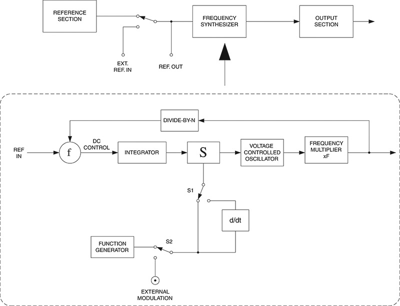
FIGURE 3.
Phase modulation, on the other hand, is sometimes generated by using a reactance modulator to vary the phase of the oscillator signal.
Sweep Generators
Sweep generators (“sweepers”) are used to produce a signal that changes frequency over a specified range. Although the sweeper nominally resembles an FM generator, there are differences. For one thing, the sweep range is usually quite a bit larger than the deviation of an FM signal generator. Another thing is that the sweeper tends to change frequency from one limit to the other, and then snaps back to the first limit.
There are three basic forms of sweep: linear (or “ramp”) sweep, stepped sweep, and list sweep. All of these forms use a voltage-controlled oscillator frequency synthesizer, but the difference is in the waveform used for sweeping the output signal. Figure 4A shows linear sawtooth waveform sweep. At time T1, the ramp applied to the VCO is at zero and begins ramping up. The frequency begins to move upwards from the zero-volts value in a linear manner until time T2, at which point it snaps back to the zero-volts value.
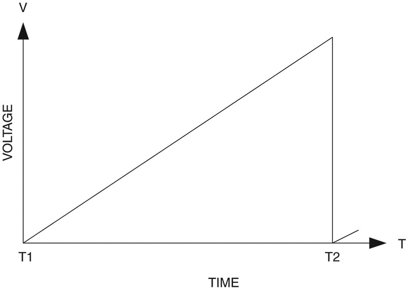
FIGURE 4A.
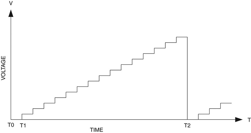
FIGURE 4B.
Stepped sweep (Figure 4B) uses a series of discrete voltage steps to change the frequency of the VCO. This method does not produce an output on every frequency in the output voltage range from T1 to T2, but rather only at specific values determined by the steps. The steps are produced in a circuit such as shown in Figure 5.
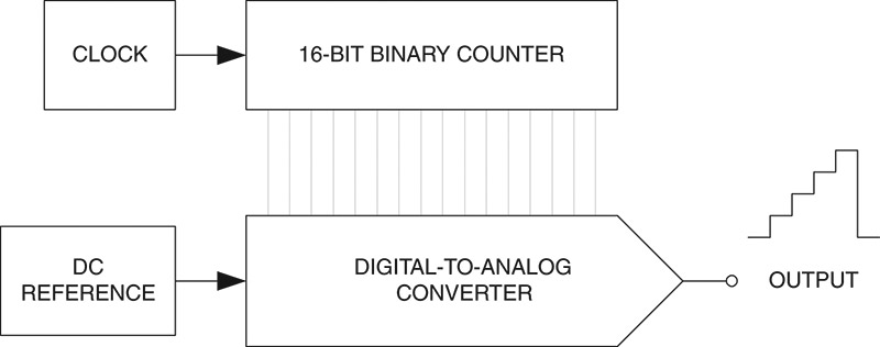
FIGURE 5.
A digital-to-analog converter (DAC) produces an output voltage that is proportional to the binary number applied to its inputs. The maximum output voltage is set by an internal or external DC reference voltage, and the applied binary number. In this case, the DAC input is driven by a binary counter which, in turn, is incremented by a digital clock (square wave generator).
The maximum number of steps that can be accommodated using any given binary counter is 2N, where N is the bit length of the counter. For the 16-bit counter shown in Figure 5, therefore, a total of 216 = 65,536 different levels (including zero) can be created. The maximum output voltage is less than the reference voltage by the 1-LSB (least significant bit) voltage, or 1/2N. If a 16-bit counter is connected to a DAC with a 10.00 volt reference source, then the 1-LSB step is 0.00015 volts and the maximum output voltage is 10.00 - 0.00015 volts = 9.99985 volts.
Output Reverse Power Protection
Many signal generators are used to test radio communications transceivers. These devices contain both transmitter and receiver, which share a common output connector to the antenna. If the signal generator is connected to the antenna connector to test the receiver, and someone accidentally keys the transmitter, then serious damage can result to the signal generator. High quality instruments provide architectures with output reverse power protection. This circuitry will prevent damage to the signal source if a high RF power level is applied to its output connector.
Digital sweepers also have a DAC to control the VCO, but will drive it with a series of values stored in a digital memory similar to those used in computers. This permits arbitrary waveforms to be created.
Figure 6 shows one way sweepers are built: open loop.
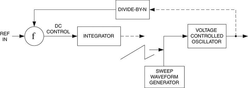
FIGURE 6.
The frequency synthesizer loop is broken, and a linear sawtooth, stepped waveform, or list generated waveform is applied to its DC control voltage input. Another approach is shown in Figure 7.
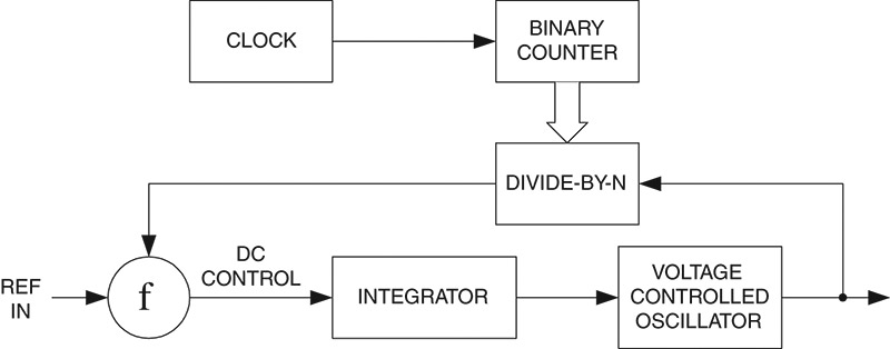
FIGURE 7.
This is a closed loop approach. The frequency synthesizer loop is not opened, but rather a binary counter or list memory is used to drive the divide-by-N counter in the synthesizer PLL feedback loop. NV