Learn how to turn your junk box orphans into a construction project or replacement part treasures.
Yes, Michael, there is such a thing as a generic logic chip.
Straight from the "It never fails" files. Ten o'clock Saturday night. You're putting the finishing touches on your mindboggling new robot steering controller. Visions of Bot Wars games numb your senses. Just one more step, a simple RS flip-flop, and your beast will roar into action. But wait! The IC cupboard is ... well, bare. Not a flip-flop in sight!
Not to fret, though. If you have just a single NOR or NAND chip in that rat's nest, you have the makings of an RS flip-flop. In fact, you probably have more logic functions in there than you're aware of.
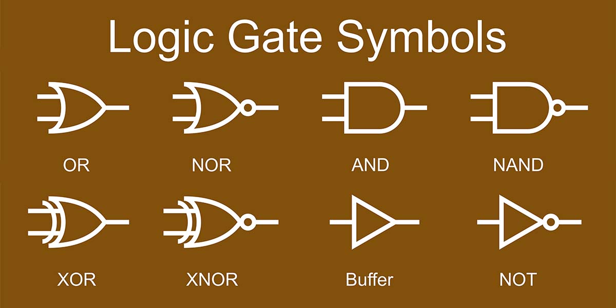
All logic circuits — no matter how complex (including that BASIC Stamp microcontroller) — are based on two elementary propositions: AND and OR. Throw in an inverter gate (NOT), and you can solve any logic equation.
In this article, I'll show you how to use these basic building blocks to get you out of a parts jam, whether it be for a new project or as a replacement device. You will also learn about the subtle differences between seemingly similar logic functions, so that you can choose the flavor that best suits your pet project.
The Basics
Boolean algebra is the basis for all computer logic. Originally formulated by George Boole, an English mathematician (1815-1864), Boolean algebra describes propositions whose outcomes are either true or false. In computer work, the true and false statements are represented by the output state of an electronic circuit, whose state can be either 1 (true) or 0 (false). We perceive these logic changes as voltage levels. That is, when the logic level is supposed to represent a 1, the output voltage will typically measure five volts. Conversely, a logic 0 is represented by — what else? Zero volts. This is important. Logic 1 is five volts and logic 0 is no volts. (Okay, you nitpickers. Before you pluck my pupils out, let me say that voltages other than five volts can represent a logic 1, with 3.3 volts being the newest inductee.)
The basic operators are AND, OR, and NOT. AND is the product of the two arguments; that is, if both propositions are true, then the statement is true. If either of the propositions is false, then the statement is false. OR is the sum of the propositions. If either proposition is true, or both are true, then the statement is true. NOT is the inverse or complement of a statement. If the statement is true, then its complement is false.
Expressed algebraically, the Boolean equations are:
| Expression |
Proposition |
Statement |
| x • y |
x AND y |
true |
| x + y |
x OR y, x AND y |
true |
| x̄ • ȳ |
NOT x AND NOT y |
true |
| x̄ + ȳ |
NOT x OR NOT y, |
|
| |
NOT x AND NOT y |
true |
The inverse function is an important logic operator because it can be used to simplify otherwise complex functions, and is sometimes the only way to arrive at a solution. For example, it's virtually impossible to solve the equation of
x OR y, but not x AND y
(the logical reasoning of an exclusive OR gate) without the NOT operator. And without the exclusive-OR gate, computers wouldn't be smart enough to add or subtract. Figure 1 shows the logic chips that we'll use for the rest of this discussion, and Figure 2 shows their elementary structures.
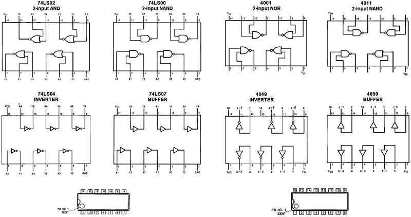
Figure 1. All the logic chips you'll ever need to build any TTL or CMOS digital project.
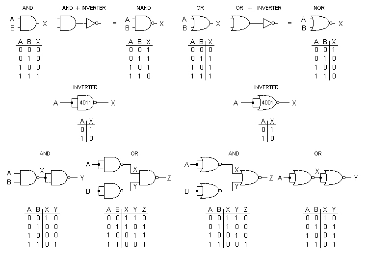
FIGURE 2. The basic binary building blocks: AND, OR, and INVERTER.
Early logic gates were built on RTL (resistor-transistor logic) technology, which was plagued by noise, blatantly cantankerous, and downright slow. RTL construction techniques of the time also limited the gate types to the simpler AND, OR, and inverter functions. It wasn't until the advent of TTL (transistor-transistor logic) that more complex designs could be successfully fabricated.
The advances included multiple inputs beyond four propositions, stable edge triggering, and increased fan-out capability. But none were more important than the paradigm shift from positive (AND/OR) logic to negative (NAND/NOR) logic thinking (Figure 3). Negative logic simplifies many Boolean equations, which leads to a reduced gate count — which results in very sophisticated logic products like embedded microcontrollers and Pentium processors.
FIGURE 3. The AND-OR and exclusive-OR gates are a perfect example of complex logic functions, made from negative logic gates, that find widespread use in the computer industry.
Negative logic isn't hard to understand, but it takes a nimble mind to implement it efficiently. In this discussion, there is a heavy emphasis on negative logic and the clustering of gate types to reduce IC count. Most logic ICs contain two or more identical gates, many of which might go unused if you don't know how to wire them to perform operations other than for what they were intended. For example, an unused NAND or NOR gate can easily substitute for an inverter, which could possibly eliminate an extra IC and make the product less costly and more reliable.
I Remember, Too
Logic gates can also be used as memory elements. In order for a logical circuit to remember and retain its logical state after the controlling input stimulus has been removed, it's necessary to include some form of feedback. This is easily done using a pair of inverters, each having its input connected to the output of the other, like the cross-linked circuit in Figure 4.
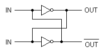
FIGURE 4. In order for a logical circuit to be used as a memory cell, it's necessary to include some form of feedback. By cross-linking the outputs of two inverters to its opposite inputs, the circuit forms a stable memory retention element.
Because the gates are inverting, the outputs will always have an opposite logic level of the input. Depending on which gate assumes control on power-up, this circuit will latch up in one of two states. To toggle between these states, an extra input is added to the cross-linked inverters, like the NAND latch shown in Figure 5a.
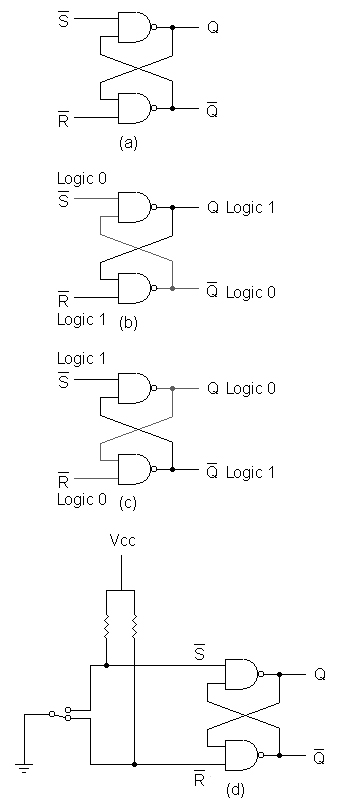
FIGURE 5. An RS latch can be used to debounce mechanical switches, sending a single, clean digital pulse to the next circuit.
The inputs are traditionally designated S and R for Set and Reset, respectively, and the outputs are designated Q and /Q The designations S and R are a logical evolution, but what prompted the use of Q for an output? Legend has it that the early memory gates weren't totally reliable, and so researchers labeled the predicted outcome as Questionable (so the story goes). In a commercial latch circuit, either or both outputs may be available for use by other circuits.
For the NAND latch circuit, both inputs should normally be at logic 1. Pulling the top gate's input low (logic 0) forces its output high (logic 1). This logic 1 is also applied to the input of the bottom NAND gate, forcing that output low (logic 0). This, in turn, feeds back to the second input of the original gate, thereby closing the feedback loop. The gates are now locked (Figure 5b), even if the /S input signal is removed. Applying logic 0 input to the top gate will have no further effect on this circuit. However, applying a logic 0 to the bottom gate will cause the same reaction in the other direction, thus changing the state of the latch (Figure 5c). If you need to switch states on a positive note, pulling the inputs high (logic 1) instead of low (logic 0), a NOR gate may be substituted for the NAND gate.
Note that it's forbidden to have both NAND inputs at a logic 0 level at the same time (the opposite occurs in the NOR latch configuration). That state will force both outputs to a logic 1, overriding the feedback latching action. In this condition, whichever input goes to logic 1 first will lose control, while the other input (still at logic 0) controls the resulting state of the latch. If both inputs go to logic 1 simultaneously, the result is a "race to the finish line" frenzy, and the final state of the latch cannot be determined ahead of time.
Pardon My Hiccups
RS latches are the most simple-minded of the flip-flop family — but that doesn't prevent them from contributing to the digital community. RS latches are often used to eliminate contact bounce in mechanical switches. When you press the button or change a switch's position, the physical contacts flex a little, causing them to make and break several times before settling down. You don't notice this when turning on a light in your home, but digital circuits are fast enough that they do notice this behavior and mimic it faithfully.
The solution is to insert an RS latch between the mechanical switch and the following circuitry, as shown in Figure 5d. Notice that the unconnected input is held at a logic 1 via a pull-up resistor, while the switched input is held at logic 0 by a direct connection to ground. (The resistor prevents the switch from shorting Vcc to ground.) When the switch is moved to its alternate position, the gate toggles to its opposite state and latches in place; additional bounces will have no effect on the output. This eliminates the contact bounce and sends a single, clean digital pulse to the next circuit.
While RS latches are useful devices, they have their limitations. One problem is how to control when the latch is allowed to change state, and when it's not. This is necessary if we have a group of latches and want to be sure they all change state (or not) at the same time. By adding a pair of NAND gates to the input circuits of the RS latch, we accomplish two goals: normal rather than inverted inputs, and a third input common to both gates which we can use to synchronize this circuit with others of its kind.

FIGURE 6. The RS NAND latch is created by adding a pair of NAND gates to the input circuits of a basic RS latch.
The gated RS NAND latch (Figure 6) circuit is very similar in operation to the basic latch. The S and R inputs are normally at logic 0, and must be changed to logic 1 to switch the state of the latch. However, with the third input, a new factor has been added. This input is typically designated clock or CLK, because it's typically controlled by a clock circuit of some sort, which is used to synchronize banks of these latch circuits with each other. The output can only change state while the CLK input is a logic 1. When CLK is a logic 0, the S and R inputs have no effect.
Flip-Flops, Not Pop-Tops
Although the gated RS latch solves some of the problems of basic RS latch circuits, and allows closer control of the latching action, it's by no means the last word. The RS latch circuit could easily experience a change in S and R input levels while the CLK input is still at a logic 1 level. This allows the circuit to change state many times before the CLK input returns to logic 0.
A good way to make sure that the latch can only change its outputs exactly on the clock cycle trigger is to sample the inputs on the transition, or edge, of the clock signal. To adjust the gated RS latch for edge triggering, we must use two identical gated latch circuits, each of which operates on opposite halves of the clock signal. The resulting circuit is commonly called a flip-flop, because its output can first flip one way and then flop back the other way. The two-section flip-flop is also known as a master-slave flip-flop, because the input latch operates as the master section, while the output section is slaved to the master during half of each clock cycle.
The edge-triggered RS NAND flip-flop is shown in Figure 7. As previously described, the circuit actually consists of two identical RS latch circuits, with an inverter connected between the two CLK inputs to ensure that the two sections are enabled during opposite half-cycles of the clock signal. The inverter is the key to the operation of this circuit.
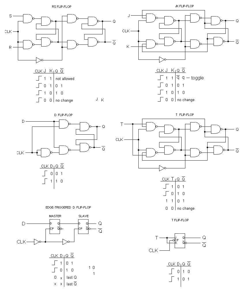
FIGURE 7. Flip-flops come in a wide variety of sizes, shapes, and features.
If we start with the CLK input at logic 0, the S and R inputs are disconnected from the input (master) latch. Therefore, any changes in the input signals cannot affect the state of the final outputs. When the CLK signal goes to logic 1, the S and R inputs are able to control the state of the input latch, just as with the single RS latch. At the same time, though, the inverted CLK signal is applied to the output (slave) latch and prevents the state of the input latch from having any effect here. Therefore, any changes in the R and S input signals are tracked by the input latch while CLK is at logic 1, but are not reflected at the Q and /Q outputs.
When CLK falls again to logic 0, the S and R inputs are again isolated from the input latch. At the same time, the inverted CLK signal now allows the current state of the input latch to reach the output latch. As a result, the Q and /Q outputs can only change state when the CLK signal falls from a logic 1 to logic 0. This is known as the falling edge of the CLK signal; hence the designation "edge-triggered flip-flop."
By making the flip-flop edge-triggered, we can precisely control the moment when all flip-flops will change state. This arrangement also allows plenty of time for the master latch to respond to the input signals, and for those input signals to change and settle down following the previous change of state.
JK Flip-Flop
Still, there is one problem left to solve: the ambiguous output condition which may occur if both the S and R inputs are at logic 1 when the CLK falls from logic 1 to logic 0. In the example above, we automatically assume that the master latch will end up in the logic 1 state — but this isn't always a certainty with real components. Therefore, we need a way to prevent a race between the two gates to see which one reaches logic 1 state first.
The solution is to add extra feedback from the slave latch to the master latch. This modified latch is called a JK flip-flop. To prevent any possibility of a "race" occurring between the R and S inputs when both inputs are at logic 1, we must somehow prevent one of the inputs from having an effect on the master latch. At the same time, we still want the flip-flop to be able to change state on each falling edge of the CLK input if the input logic calls for it. Whether the S input or the R input is to be disabled depends on the current state of the slave latch outputs. If the Q output is a logic 1 (the flip-flop is in the Set mode), the S input can't be any more set that it already is. Therefore, the S input can be disabled without disturbing the flip-flop under these conditions. In the same way, if the Q output is logic 0 (the flip-flop is Reset), the R input can be disabled without causing any harm. We have thus prevented a foot race to logic 1.
Feedback control of the RS flip-flop inputs is attained by adding two new inputs from the Q and /Q outputs. (Remember that NAND and NOR gates may have any number of inputs.) To prevent confusion, the designations of the new flip-flop inputs are designated J (instead of S) and K (instead of R).
In most ways, the JK flip-flop behaves just like the RS flip-flop. The Q and /Q outputs will only change state on the falling edge of the CLK signal, and the J and K inputs will control the future output state pretty much as before. However, there are some notable differences.
Since one of the two logic inputs is always disabled, the master latch can't change state back and forth while the CLK input is at logic 1. Instead, the enabled input can change the state of the master latch once. This isn't true of the RS flip-flop. The Q and /Q outputs can only change state with each falling edge of the CLK signal, with the master latch circuit changing state with each rising edge of CLK.
We can use this characteristic to our advantage in a number of ways. A flip-flop built specifically to operate this way is typically called a T flip-flop (Toggle flip-flop). The lone T input is, in fact, the CLK input for other types of flip-flops.
The operation of the T flip-flop is identical to that of an RS flip-flop with joined S (set) and R (reset) inputs. Every T input pulse triggers switching of the latch to the opposite state. When it's in logic 0, a CLK pulse changes the T flip-flop to the logic state 1. When the latch is in logic 1, a clock pulse changes the flip-flop to logic state 0. Note that the frequency of the output pulses is exactly half of the frequency of the input pulses.
D Flip-Flop
One very useful variation on the RS latch circuit is the Data latch, or D flip-flop, as it's generally called. The D flip-flop is constructed by using the inverted S input as the R input signal. The single remaining input is designated D to distinguish its operation from other types of latches. It makes no difference that the R input signal is effectively clocked twice, since the CLK signal will either allow the signals to pass both gates or it won't.
When the CLK input is logic 1, the Q output will always follow and reflect the logic level present at the D input, no matter what course it may take. However, when the CLK input falls to logic 0, the state of the D input at that instant is trapped and held in the latch for use by whatever other circuits may need this signal. Because the single D input is also inverted, this latch circuit can't experience an ambiguous state condition caused by all inputs being at logic 1 simultaneously, making it safe to use in any circuit.
Although the D flip-flop doesn't have to be edge-triggered, there are some applications where an edge-triggered D flip-flop is desirable. This can be accomplished by using a D latch circuit as the master section of an RS flip-flop. Both types are useful, and both are commercially available.
With all of these different types of latches and flip-flops, the logic diagrams we've been using have gotten rather large, especially for the edge-triggered flip-flops. Fortunately, it really isn't necessary to follow and understand the inner workings of any of these circuits when they are used in larger applications. Instead, we used a set of very simple symbols to represent each type of latch or flip-flop in larger logical circuits, as shown in the two bottom circuits of Figure 7.
That's all for this installment. Coming next time is a look at the brainier side of binary logic. Here is where we put the above logic gates and memory cells to work on mathematical problems. NV