A Necessary Device for the Modern IC
The commonly used bipolar transistor — in which electrons or holes pass through two PN semiconductor junctions — is essentially a current amplifying device. Although voltage can be amplified indirectly if the “common emitter” or “common collector” wiring configurations are used, it still is true that a small amount of input current must always flow into the transistor’s base region for control purposes.
Another type of semiconductor device, the field effect transistor or “FET,” is not as familiar to many electronics hobby enthusiasts, possibly because it is easily damaged by misuse. The FET amplifies voltage directly, and the current needed for control is so low that it cannot be measured with common instruments. This transistor was actually the first type of semiconductor amplifier predicted theoretically at Bell Labs, back in the 1950s, but it was not developed into a practical device until after the bipolar type had become popular. However, FETs have now become the most common type, with tens of millions of them in each microprocessor IC chip.
With such a huge number of transistors operating in a single chip, we certainly don’t want much current to be required for the control of each one — the battery power would be used up fast, and a lot of heat would have to be removed. Also, there are many other applications where super-low input current is desirable. An obvious example is in the first stage of an accurate voltmeter, where we don’t wish to cause any new voltage drops by draining current out of the circuit being studied.
Still another advantage of the FET, probably less important, is the fact that its input versus output characteristics are similar to those of vacuum tubes. Because tubes have been used since about 1910, we have a great deal of experience with them, and some designers feel more comfortable with FETs than with bipolar devices, especially in audio amplifiers. (Whether or not this is truly an advantage borders on emotional factors as much as scientific ones. Some readers might recognize the author of the present article as an early partisan on one side of this intensely debated issue, so we won’t discuss it any further here!)
At any rate, the FET responds entirely to voltage at the controlling electrode, and this can be used to throttle fairly large amounts of output current and/or voltage in the other two wires.
The JFET
Instead of making a transistor that conducts through both PN junctions when it is turned on (“bipolar”), one type of FET transistor can be made with just a single PN junction (“unijunction”). Since it does have a junction, it is called a juncFET or JFET, and a simplified cross section diagram is shown in Figure 1.
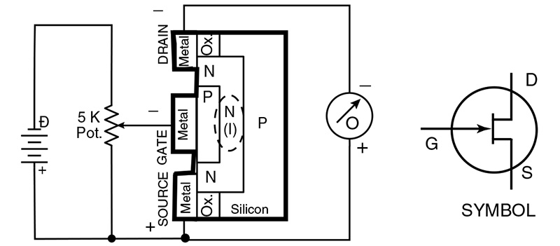
FIGURE 1. Simplified cross section of a JFET, with an operating circuit. It is N-channel, depletion mode, and normally on. The symbol is at the right-hand side of the figure.
The rectangles enclosed by a thick line are solid materials, including two regions that are P-type silicon but do not conduct appreciable current. There is an N-type region in the middle that can conduct all the current. In the very simple circuit shown in the diagram — which the reader can easily construct to get some experience with the JFET — an ohmmeter provides a voltage and also indicates a flow of load current. This type of FET is normally in the turned-on state, before any control voltage is applied. If the 5K potentiometer is set so there is no voltage on the “gate” (by sliding its arrow downwards as shown in the diagram), then “positive” load current from the ohmmeter goes into the upper left corner of the FET, then down into the topmost metal, then down through the continuous N-type silicon, and out of the transistor through the lower metal. (The “Ox.” regions are silicon dioxide insulators.)
The diagram is not drawn to scale, and the rectangles show regions that are actually only about a micron in size. (A more formal size designation is “micrometer,” which is a millionth of a meter.) The metal is usually a thin aluminum or copper film about a micron thick, and the whole configuration is sometimes more complex than shown in this simplified diagram. The P-type silicon (to the right, as drawn here) is mainly just a mechanical support for the smaller active regions that do the conducting. It is often referred to as the “substrate.”
To turn off the transistor, the 5K pot setting can be raised to provide a negative control voltage. This charges the P-type region, but practically no electricity actually flows, because there is a “reverse-biased” PN junction (negative voltage on P-type silicon and positive on N). However, this charge strongly repels electrons from the very thin N-type conductive “channel” in the middle. A depletion zone conaining fewer electrons is formed there, so the silicon inside the dashed-line oval becomes intrinsic (I-type, as symbolized by the I in parenthesis), which is insulating, and the FET stops conducting. This type of behavior is called “depletion mode.” Because the controlling action is done by an electric field (and not by carriers flowing into a base region), the whole device is called a field effect transistor, or “FET.”
One metal electrode is called the source, one is the gate, and one is the drain, similar to the emitter, base, and collector in a bipolar transistor. This is an “N-channel” device, because the current goes through N-type silicon. The symbol is shown to the right of the cross section. Another type of JFET, a “P-channel” device, has the opposite types of P and N semiconductor regions, so the arrow in the symbol is aimed away from the channel. That type of gate must be charged positive in order to turn off the channel by repelling holes. It is not as common as the one shown here, but it does exist, and it can be useful for special purposes.
Constant Current Diode
An interesting application for the JFET is in the “constant current diode.” The total effect of this is similar to that of a bipolar voltage regulator, except that current is regulated here instead of voltage. This can be a very simple circuit, as shown in Figure 2, diagram B.
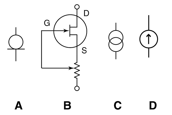
FIGURE 2. An N-channel JFET wired to be a constant current self-regulating device, with the symbol shown next to it on the left. The other two symbols, to the right, are for constant current sources that include power supplies such as batteries.
Looking at the negative current that flows upward through the resistor, some of it will be sent to the gate, which partially turns off the FET. This is negative feedback, so if the current in the circuit starts to increase, then the transistor gets turned off even more. Thus, less current flows, until some constant current level is reached. The JFET and potentiometer are all inside an insulating plastic “package.” That whole thing, plus a power source like a battery (not shown here), is symbolized by two overlapping circles, Figure 2, diagram C. Occasionally an alternative symbol is used, with an upward arrow, especially in Europe, as shown in diagram D.
The MOSFET
A different kind of field effect transistor is illustrated in Figure 3, the metal-oxide-semiconductor or “MOS” device.
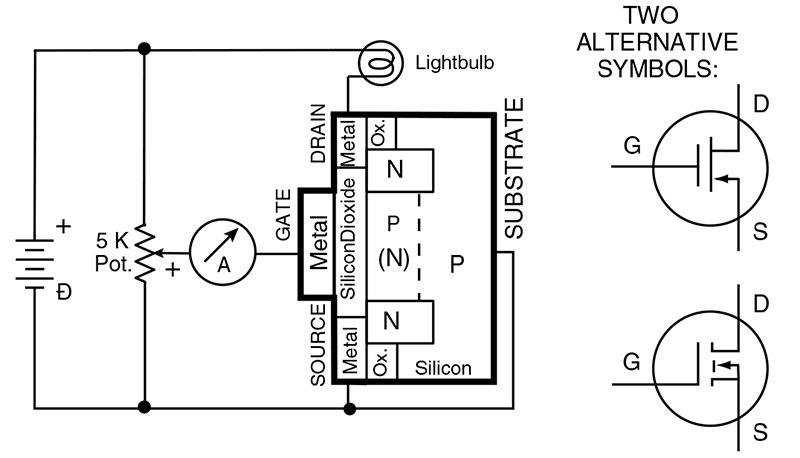
FIGURE 3. Simplified cross section diagram for a MOSFET, with an operating circuit. It is N-channel, enhancement mode, and normally off. Two alternative symbols are shown at the right.
In this transistor, there is insulating silicon dioxide to prevent gate current from going into the main semiconductor, instead of the reverse-biased junction that was used in the JFET. This one is sometimes called an “IGFET,” because of the insulated gate. It is a normally off device, which has to be turned on by some sort of action, and therefore it is referred to as an “enhancement mode” device. (The IGFET can also be made in a depletion mode configuration.)
In the figure, if the pot is turned down to zero voltage, then the battery current tending to go through both the lightbulb and the transistor will be stopped by one of the PN junctions. In this diagram, it is the upper one, which is reverse-biased. (Initially, the dashed line and the N region in the middle are not present.)
If the potentiometer arrow is raised, and a positive potential is now applied to the gate, holes in the P-type silicon are repelled, causing this region to become N-type (as indicated by the N in parenthesis). Now there is no PN junction directly in the path between the upper and lower N-type regions, because it is all one continuous N-type region (drawn as a vertical bar, with the dashed-line as one edge). This transistor is also N-channel, because the electricity goes through N-type silicon when it is turned on.
If the reader wishes to get some experience with the MOSFET, an ammeter can be placed as in Figure 3, to show that no measurable current flows into the gate, even when the bulb is lit. In this diagram, the multimeter has been switched to measure current, and it is moved to the gate lead. (This circuit could be used for the JFET experiment also. The experimenter should note that precautions for avoiding damage to MOS devices are described in the ESD Sensitivity section below.)
Symbols for the MOSFET are shown on the right. The arrow, in this case, indicates that the “source” electrode is internally connected to the substrate, which is often done if one of the PN junctions is not going to be used.
If the device were P-channel, the source and drain would be P-type, and the arrow would be aimed away from an N-type substrate.
Characteristic Curves and Load Line
Typical FET “spec sheets” use formats similar to those of vacuum tubes. The shapes of the curves are almost the same, but the voltages are usually much lower. The input is the VGS and the output is the ID. In this case, a type 2N7000 MOSFET is used in N-channel enhancement mode.
A “load line” is shown here as a dashed line. Its slope represents the effect of a load resistance (such as the lightbulb in Figure 4), and it is quite valuable as a way to show the amount of current in any situation.
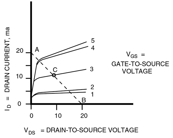
FIGURE 4. Characteristic curves for a 2N7000 MOSFET, with a load line.
In the case graphed here, the load resistance is 1,000 ohms, and VDS is 20 volts. The dashed load line is drawn from the maximum possible voltage (shown here as B) to the maximum possible current with that particular load, which is 20V/1KW = 20 mA (shown as A). If the transistor is turned partly “on” (VGS = 3 volts), the drain current would be about 11 mA, as shown by the intersection (the circle under the letter C).
CMOS
Two MOS transistors of opposite type can be wired as in Figure 5, in the complementary MOS configuration (“CMOS”).
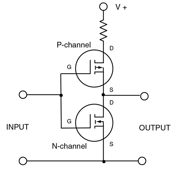
FIGURE 5. CMOS transistor pair. The current is extremely low when there is no input signal.
When no signal is fed to the input, one of the transistors is always “off,” so essentially zero current can get from the power supply down through the resistor, and then through the pair of transistors. When a signal comes to the input, then load current can be drawn from the output terminal, at either high (V+) or low (ground) voltage, depending on the polarity of the input voltage. However, in the situations when there is no input, the overall current is practically zero.
Modern integrated circuits have millions of transistors attached in parallel, so if only a microamp of “leakage current” flowed through each one that was not being used, an ampere or more would still be drawn from the power supply or battery at all times. That would generate a lot of heat and also drain batteries too fast for portable devices. Therefore, almost all modern calculators, laptop computers, cellular phones, etc., use CMOS circuits whenever possible.
ESD Sensitivity
The MOS transistor is particularly susceptible to damage from static electricity, of the kind generated when a person walks across a rug in dry weather. The spark that the person makes when touching the metal faceplate on a light switch is called electrostatic discharge, or “ESD,” but damage can be done to a MOSFET, even if there is not enough static to make a visible spark.
Static electricity can destroy the very thin silicon oxide that insulates the gate. Some MOS transistors are protected by zener diodes that are attached in parallel with them, inside the packages, but most are not protected. To prevent damage, people handling IGFETs should always follow these two precautions:
- Only touch the plastic insulation with your hands, not the metal leadwires directly;
- Use a grounded wrist strap.
The latter is a plastic band (usually black or pink) that conducts electricity and is attached to a long wire. It should be fastened around either wrist, touching the person’s skin, and then the other end of the wire is hooked up to a good ground connection such as a water pipe. NV
Parts List
| JFET |
N-channel |
| Potentiometer |
5,000 ohms |
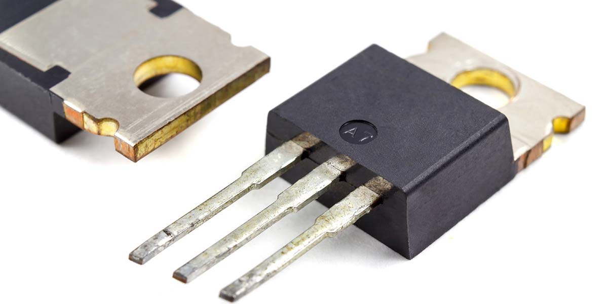
| Power MOSFET |
N-channel |
| Lamp bulb |
Tungsten, 12 volt, 40 mA |
| Battery |
Nine-volts |
| Multimeter |
|
| Static-grounding wrist strap |
|