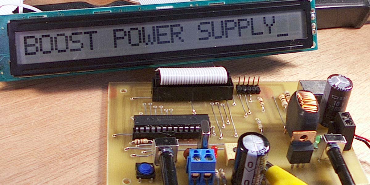
Can you generate 200 volts DC from a five-volt DC PIC power supply? Yes, you can, and I will tell you how. In this two-part series, we will build a 200-volt DC boost power supply driven by an 18F2455 Microchip PIC microprocessor. The completed power supply (shown in Figure 1) will generate between five and 200 volts DC from a five-volt, DC input.
FIGURE 1. Completed boost power supply.
This device can be used for any application where high voltage and low current is needed, such as PIC programming (13 volts), neon indicator bulbs (120 volts), or nixie tube displays (170 volts).
In this first part, we’ll cover the theory of how a boost power supply works. You’ll learn how to use pulse width modulation (PWM) to get the 18F2455 PIC to output a square wave with a given period and duty factor, and we’ll look at how the PWM’s “ON” time affects voltage. We will cover the important parameters in designing a boost power supply and use the free LTSPICE program to come up with a possible design.
In the second article, we will implement this design on a printed circuit board. We will use a liquid crystal display (LCD) to show important power-supply parameters. Using a free C compiler, we’ll write software to drive A/D conversion, control PWM, and output information to the LCD.
Boost Power Supply Theory
A boost power supply is a type of switching power supply that generates a higher output voltage than the supply voltage. In addition to stepping up the voltage, it can also change the sign of the voltage input. These tricks are very useful for generating a local source of other voltages from a standard +5 VDC supply.
A boost converter can have as few as four basic components: a semiconductor switch, a diode, an inductor, and a capacitor. The semiconductor switch may be a unipolar device, such as a MOSFET, or a bipolar transistor. The benefit of using a unipolar device is the absence of stored carriers and, therefore, theoretically instantaneous switching transients that are limited only by small parasitic capacitances.
If you are like me, you may not have a large assortment of inductors in your parts box and you may not use them a lot in your circuits. Let’s take a more detailed look at inductors. Inductance (measured in Henries) is an effect which results from the magnetic field that forms around a current carrying conductor. Inductance can be increased by looping the conductor into a coil which causes magnetic flux from adjacent loops of the conductor to link.
An inductor is usually constructed as a coil of conducting material, typically copper wire, wrapped around a core of ferrous material, which is highly permeable to magnetic flux. The coils and the core’s permeability amplify the current’s magnetic field, increasing inductance. Some small inductors look similar to resistors and use a similar color scheme. Other inductors look like wire-wrapped donuts (toroids), as shown in Figure 2.
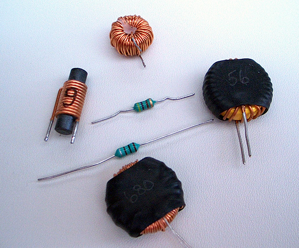
FIGURE 2. An inductor assortment.
Two (or more) inductors that have coupled magnetic flux form a transformer — a fundamental component of every electric power grid. An inductor is used as the energy-storage device in the boost power supply. The inductor is energized for a specific fraction of the regulator’s switching frequency — the “ON” time — and de-energized for the remainder of the cycle. When we select the inductor to use in our boost power supply, we want to make sure the inductor can handle the peak current. The peak current in the inductor of the boost power supply can be written as a function of the input voltage, semiconductor ON time, and inductance:
Max_Current = Input_Voltage* ON_Time/Inductance
The basic circuit is shown in Figure 3 and operates as follows:
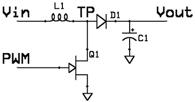
FIGURE 3. Basic boost power supply schematic.
- The inductor current ramps up while the MOSFET is conducting (TP voltage near zero). When the MOSFET is conducting, the source voltage is applied across the inductor, and the rate of rise of inductor current depends on the source voltage Vin and inductance L1. If the source voltage remains constant, the rate of rise of inductor current is positive and remains fixed, so long as the inductor has not saturated.
- When the MOSFET is off, the voltage at TP rises rapidly as the inductor tries to maintain a constant current. The diode turns on, and the inductor dumps current into the capacitor, increasing the output voltage to more than the input voltage.
- The switching of the MOSFET will be controlled by a microprocessor using PWM. PWM will control the duty cycle, D, which is the fraction of the time the output is high. The value of D varies such that 0 < D < 1. The output voltage is lowest when D = 0. At zero D, the output voltage equals the source voltage. As D approaches unity, the output voltage tends to infinity. Usually D is varied such that 0.1 < D < 0.9.
A boost power supply can be driven in discontinuous conduction mode (DCM) or continuous conduction mode (CCM), depending on whether the current in the inductor is allowed to go to zero or not. In DCM, the semiconductor is switched on only after the inductor current has fallen to zero. In CCM, the switch is turned on before the current through the diode reaches zero. We will operate in DCM because we want to have the largest range of duty cycles. Also, the equations for DCM are somewhat simpler. The basic waveforms for DCM are shown in Figure 4.
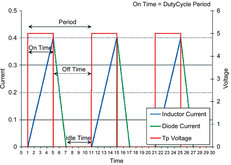
FIGURE 4. Showing boost power supply waveforms.
[Reference 1] gives the following equation for the boost power supply output voltage, in DCM, as a function of the input voltage, load resistance, semiconductor ON time, period, and inductance:
Output_Voltage = Input_Voltage*(1 + SQRT(1+(4*On_Time/Period))/K)/2,
where
K = 2*Inductance/(Output_Load_Resistance * Period)
A spreadsheet to calculate the output voltage, peak current, current fall time, and other important boost power supply parameters is available in the downloads section at the end of this article. I generated Figure 5 using the spreadsheet, but it assumes a perfect inductor. One can use the spreadsheet to see the effects of inductor value, ON time, voltage ripple, and load on the peak current, output voltage, and output capacitor.
| BOOST CALCULATOR |
| INPUT |
| INDUCTOR |
220.00 |
µH |
| ON TIME |
24.00 |
µsec |
| PERIOD |
32.00 |
µsec |
| VIN |
5.00 |
volts |
| INDUCTOR EFF |
70.00 |
% |
| R3 |
330000.00 |
ohms |
| R4+R10 |
8000.00 |
ohms |
| RLOAD |
34000.00 |
ohms [1] |
| DESIRED RIPPLE |
0.02 |
volts |
| OUTPUT |
| POWER OUTPUT |
0.95 |
watts |
| SWITCHING FREQ |
31250 |
Hz |
| PEAK CURRENT |
0.55 |
amps |
| VOUT |
180.27 |
volts |
| FALL TIME |
0.68 |
µsec |
| RLOAD total |
30892.47 |
ohms |
| A/D AT VOUT |
873 |
counts |
| DC LOAD CURRENT |
0.005835 |
amps |
| FILTER CAPACITOR |
25.16 |
µF |
| [1] Equivalent to two nixie tubes. |
TABLE 1. The Boost Calculator Spreadsheet.
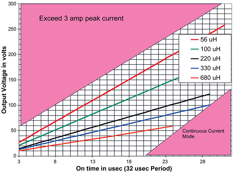
FIGURE 5. Output voltage versus ON time and inductance for a 32 µs period.
Also shown in Figure 5 are two limiting conditions. First, if the ON time and inductor combination are too large, the power supply will cease to operate in DCM and will start operating in CCM. Second, if the inductor value is too small, the peak current will exceed the limiting current of one of the components.
An Introduction to Pulse Width Modulation
Most Microchip microprocessors have a PWM feature. PWM is a process by which the ON portion of a square wave is varied as shown in Figure 4. For the PIC182455 microprocessor, the PWM output is on Pin 13 (RC2). PWM can be described by the two parameters: period and duty cycle. The period and ON time are controlled by loading certain values into registers on the microprocessor. The period is set by using the following equation:
PWM Period = (PR2+1) * 4 * Tosc *TMR2
Here, PR2 is the TIMER2 period register, and TMR2 is the TIMER2 prescaler register. Tosc is the period of the system clock, that is, (clock rate)-1. For example, for a 48 MHz clock rate, Tosc would be 1/48 (= 0.0208) microseconds.
The ON time is calculated from the following equation:
PWM ON Time = (CCPR1L:CCP1CON<5:4>) * Tosc *TMR2
where CCPR1L:CCP1CON<5:4> is a 10-bit number consisting of the contents of the CPR1L register and bits 5 and 4 of the CCP1CON register.
If the ON time is longer than the PWM period, the CCP2 output pin will never be cleared. Table 2 shows the behavior of the PWM period and ON time for various register values.
| MICROPROCESSOR FREQ |
48 MHz Tosc = 0.0208 µs |
| CCPR1L:CCP1CON(4:5) |
512 |
512 |
512 |
256 |
128 |
64 |
72 |
| TIMER PRESCALER |
61 |
4 |
1 |
1 |
1 |
1 |
16 |
| PR2 VALUE |
128 |
128 |
128 |
128 |
128 |
128 |
23 |
| PWM FREQUENCY (Hz) |
5814 |
23256 |
93023 |
93023 |
93023 |
93023 |
31250 |
| PWM PERIOD (µs) |
172.0 |
43.0 |
10.8 |
10.8 |
10.8 |
10.8 |
32.0 |
| PWM ON TIME (µs) |
170.7 |
42.7 |
10.7 |
5.3 |
2.7 |
1.3 |
24.0 |
TABLE 2. Pulse width modulation parameter table.
This table shows that increasing the product of PR2 and TMR2 increases the PWM period. Increasing the contents of CCPR1L and CCP1CON increases the ON time.
One common application of PWM signals is motor control. By varying the ON time of a PWM signal sent to a motor, you can vary the effective power of the signal and thereby slow the motor down or speed it up. We will use the PWM signal to control the voltage output of the boost power supply.
Circuit Design
In order to build the circuit, there are a number of interacting variables that need to be optimized to determine the final output voltage and the response to the requested voltage. Some of these variables are:
- Value of L1 inductor (inductor rated at peak current)
- Value of C1 capacitor (capacitor rated at peak voltage)
- PWM period
- PWM ON time
- Values of R3 and R4 to limit A/D value to 0-5 volts
Because of the number of interacting values, I decided to use the computer program SPICE to analyze the circuit before building it on a breadboard. SPICE stands for Simulation Program with Integrated Circuit Emphasis. SPICE is a general-purpose circuit simulation program developed at the University of California, Berkley for nonlinear DC, nonlinear transient, and linear AC analyses. Circuits may contain resistors, capacitors, inductors, independent voltage and current sources, and the five most common semiconductor devices: diodes, BJTs, JFETs, MESFETs, and MOSFETs.
I had not used SPICE before, but there was an excellent article in the July ‘02 issue of Nuts & Volts [Reference 2]. The LTSPICE program mentioned in the article is available as a free download at [Reference 3]. The LTSPICE program now includes the SWITCHERCAD III graphical user interface that allows one to draw a schematic and analyze it with LTSPICE without ever having to enter a SPICE command. Figure 6 shows the LTSPICE model that I arrived at after some trial and error.
The LTSPICE model shows two voltage sources. One is the five-volt DC supply. The second voltage source is described by the PULSE(0 5 0 1E-6 1E-6 24E-6 32E-6 1000000) command. The PULSE statement describes a square wave pulse that has an ON time of 24 microseconds and a period of 32 microseconds. The “.TRAN” command tells SPICE to run a 100 millisecond transient using 10 ms steps.
R1 is a load resistor standing in for the power supply load. R2 and R3 form a resistor voltage divider network that scales the output voltage to 0-5 volts.
There was no SPICE model included for the IRF730 MOSFET with the LTSPICE program package. The device vendor does have a SPICE model for the IRF730, called IRF730.SPI, which can be downloaded from [Reference 4].
There are two types of third-party SPICE models: those described with a .MODEL statement and those defined with a .SUBCKT statement. Models given as .MODEL statements are for intrinsic SPICE devices like diodes and transistors. The .MODEL statement gives the parameters for the specific component. The behavior of the device is already known by SPICE and only the parameters need to be given to finish specifying the component’s electrical characteristics. Figure 6 shows the .MODEL statement for the MBRS3201T3 Schottky diode [Reference 5].
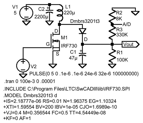
FIGURE 6. LTSPICE model of boost power supply.
In contrast, models given by .SUB CKT statements define the modeled component by a collection of circuitry of intrinsic SPICE devices. For example, the SPICE model of an op-amp would be given as a sub-circuit. The IRF730 is also described by a SUBCKT statement.
Adding an IRF730 MOSFET that’s described by SUBCKT statements to the circuit is a little tricky. It’s done as follows:
- Add an instance of symbol NMOS to your schematic.
- Move the cursor over the body of the newly placed N-channel MOSFET symbol instance and press <Ctrl>RightMouseButton. A dialog box will appear. Change Prefix: MN to Prefix: X. This causes this instance of the symbol to netlist as a sub-circuit instead of as a MOSFET.
- Edit the value “NMOS” to “IRF730” to coincide with the name given on the .SUBCKT line.
- Add the SPICE directive “.INCLUDE C:\Program Files\LTC\SwCADIII\lib\
IRF730.SPI” to the schematic to point to the file containing the SUBCKT information.
Hit the SIMULATION/RUN menu item, and the output should look like Figure 7.
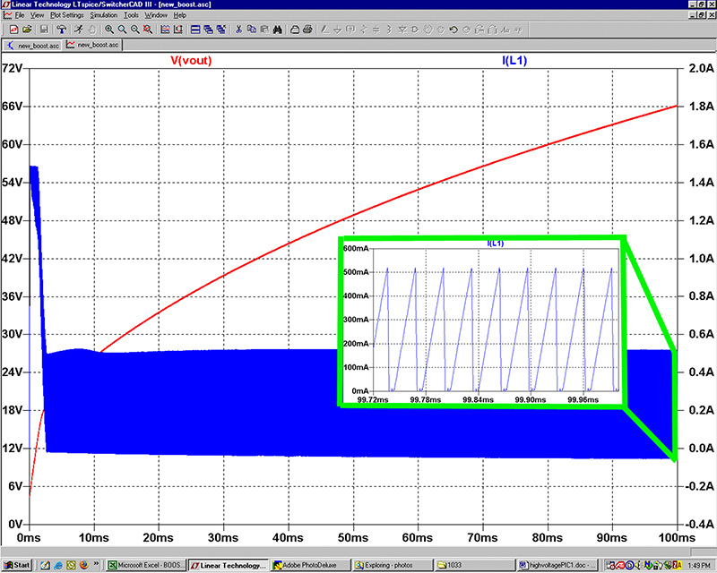
FIGURE 7. Output of LTSPICE model.
Figure 7 shows that the output voltage increases to approximately 66 volts over the first 100 milliseconds after power is turned on. If you examine I(L1), you will see that when the power is first turned on, there is a large transient in the current through the inductor. The large transient occurs if the ON time of the semiconductor switch is constant at 24 µs. We can reduce the required peak current capacity of the inductor by using a software “soft start.” In the “soft start” algorithm, ON time is initially set to zero, then increased slowly until the desired voltage is reached.
If you examine the blowup of the last part of the startup, you will see that the current through the inductor returns to zero during each power cycle. This behavior confirms that the device is operating in DCM, as expected.
The two large capacitors — C1 and C2 — are used to help reduce the ripple on the output voltage. Any switching supply, no matter how well regulated and filtered, has some ripple (also known as output noise). Without the large capacitors, the A/D conversion is unsteady and the output voltage tends to oscillate. The output ripple is not visible in the output voltage plot in Figure 7, but a close examination of the simulation reveals that it is there.
In addition to large output capacitors, ripple can be further reduced by the addition of output filters. An output filter consists of a small inductor L (2-10 µH) and a capacitor C1 (50-150 µF) in parallel with the output capacitor as shown in Figure 8.
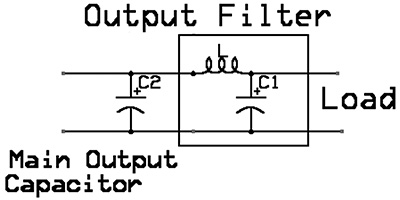
FIGURE 8. Boost power supply output filter.
The inductor must be rated at full load current since the load is connected across the output filter capacitor.
Figure 9 shows the basic PWM logic implemented on the microprocessor.
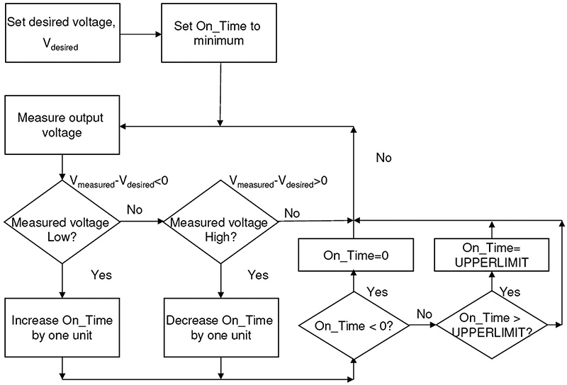
FIGURE 9. Simplified flow chart.
[Reference 6] has a more complicated algorithm that involves looking not only at the voltage error, but also at the integral of the voltage error and the derivative of the voltage error. This more complicated correction algorithm is intended to reduce voltage oscillations and improve convergence of the output voltage to the desired voltage. You may want to try it if your output voltage oscillates or fails to converge to the desired voltage.
Conclusion
This article covered the theory of how a boost power supply works. It described pulse width modulation and explained how to get the 18F2455 PIC to output a square wave with a given period and ON time. It covered the important parameters in designing the boost power supply, showed how to use the free LTSPICE program to come up with a possible design, and looked at the output of a simulation using this design.
In our next article, we will build the power supply we just designed. We will write the software needed to drive the PIC in a freely downloadable version of the C language. We will discuss the software that drives the A/D conversion, the LCD display, and the PWM. Then we will program the microprocessor with the software. I will mention some of the pitfalls in designing a switching power supply and, finally, use the power supply to power some simple applications. NV
REFERENCES
- Boost Steady State Discontinuous Mode Analysis, downloaded 11/14/2005 from http://focus.ti.com/lit/an/slva061/slva061.pdf
- A. Williams, “Spice Up Your PC,” Nuts & Volts, July 2002, pp. 10-12.
- LTSPICE Version 2.16h free 5.4 MB download (retrieved 10/5/2005) was used in the writing of this article from www.linear.com/designtools/software/#LTspice. An updated newer version is available.
- IRF730 SPICE model retrieved 10/6/2005 from www.irf.com/product-info/models/spice.
- MBRS3201T3 SPICE model retrieved on 11/9/2005 from www.onsemi.com/PowerSolutions/product.do?id=MBRS3201
- R. Condit and D. Butler, “Low Cost Microcontroller Programmer,” Microchip App Note 258, retrieved 10/21/2005 from http://www.microchip.com/wwwAppNotes/AppNotes.aspx?appnote=en012103
Downloads
High Voltage PIC 2006-09 (spreadsheet, PCB layout, and source codes)