Digital Buffer IC Circuits
Logic gate basics and a detailed look at practical TTL and CMOS digital buffer IC circuits in this first part of a five-part mini series.
Logic Gate Symbology
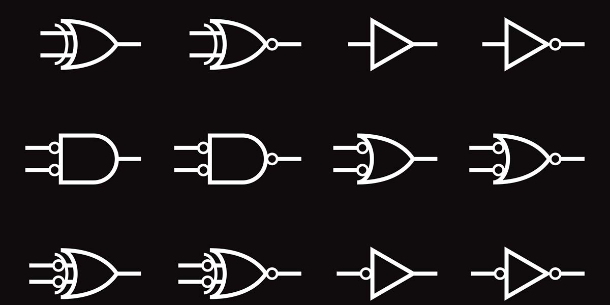
The eight best known types of digital logic gates are the buffer and the NOT, OR, NOR, AND, NAND, XOR (EX-OR), and XNOR (EX-NOR) types. Many different symbols can be used to represent each of these eight basic logic gate elements. Figure 1 shows four different families of symbols that are widely used in different parts of the world today; of these, the American MIL/ANSI symbols are by far the most popular, are instantly recognizable, are used by most of the world’s practical digital engineers, and are used throughout this series.
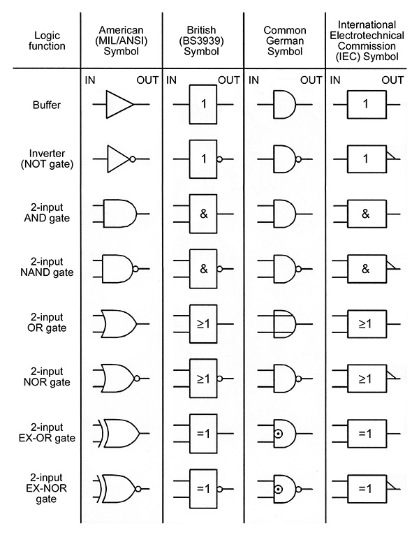
FIGURE 1. A selection of widely used logic symbols.
Two useful variations of these American symbols are also widely used and are shown added to a standard inverter symbol in Figure 2.
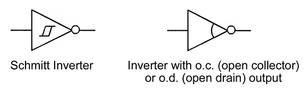
FIGURE 2. Useful variations of the MIL/ANSI inverter symbol.
The left-hand symbol is internationally recognized and indicates that the logic element has a Schmitt trigger input action; the right-hand symbol — which is widely used but is not universally recognized — indicates that the logic element has an open-drain (o.d.) or open-collector (o.c.) output stage.
Logic Gate Functions
The functional action of any logic gate can be described either in words or in a tabular or symbolic way. The following list describes the functions of all eight basic types of logic gates in words.
- Buffers — A buffer is a non-inverting amplifier that has an output drive capacity that is far greater than its input drive requirement, i.e., it has a high fan-out and gives a logic 1 output for a logic 1 input, etc.
- Inverters — An inverter (also known as a NOT gate) is a high fan-out amplifier that gives a logic 1 output for a logic 0 input, and vice versa.
- AND Gates — An AND gate has an output that is normally at logic 0 and only goes to logic 1 when all inputs are at logic 1, i.e., when inputs A and B and C, etc., are high.
- NAND Gates — A NAND gate is an AND gate with a negated (inverted) output; the output is normally at logic 1 and only goes to logic 0 when all inputs are at logic 1.
- OR Gates — An OR gate has an output that goes to logic 1 if any input is at logic 1, i.e., if inputs A or B or C, etc., are high. The output goes to logic 0 only if all inputs are at logic 0.
- NOR Gates — A NOR gate is an OR gate with a negated output; it has an output that goes to logic 0 if any input is at logic 1, and goes to logic 1 only when all inputs are at logic 0.
- XOR Gates — An exclusive-OR (EX-OR) gate has two inputs, and its output goes to logic 1 only if a single input (A or B) is at logic 1; the output goes to logic 0 if both inputs are in the same logic state.
- XNOR Gates — An exclusive-NOR (EX-NOR) gate is an EX-OR gate with a negated output, which goes to logic 1 if both inputs are in the same logic state, and goes to logic 0 only if a single input is at logic 1.
Figure 3 shows how the functions of the eight basic types of gates can also be presented in tabular form via truth tables (which show the logic state of the output at all possible input logic state combinations) or symbolically via Boolean algebraic terms. Note that, by convention, all logic gate inputs are notated alphabetically as A, B, C, etc., and the output terminal is notated as Y (in counters and flip-flops, etc., the main output is usually notated as Q).
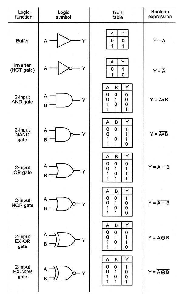
FIGURE 3. Symbols, truth tables, and Boolean expressions for the eight basic types of logic gates.
The actual logic states may be represented by 0 and 1, as shown, or by L (= Low logic level) and H (= High logic level). Also note in the Boolean expressions that a negated output is indicated by a negation bar drawn above the basic output symbol; the negated state is called a not state; thus, a negated Y output is called a not-Y output.
Positive Versus Negative Logic
All modern digital logic circuitry assumes the use of the positive logic convention, in which a logic 1 state is high and a logic 0 state is low. In the early days of electronic digital circuitry, an alternative ‘negative logic’ convention — in which a logic 1 state is low and a logic 0 state is high — was also in common use, and it is sometimes still useful to be able to think in negative logic terms, particularly when designing gates in which a low state output is of special interest. With this point in mind, Figure 4 presents a basic set of two-input positive and negative logic equivalents.
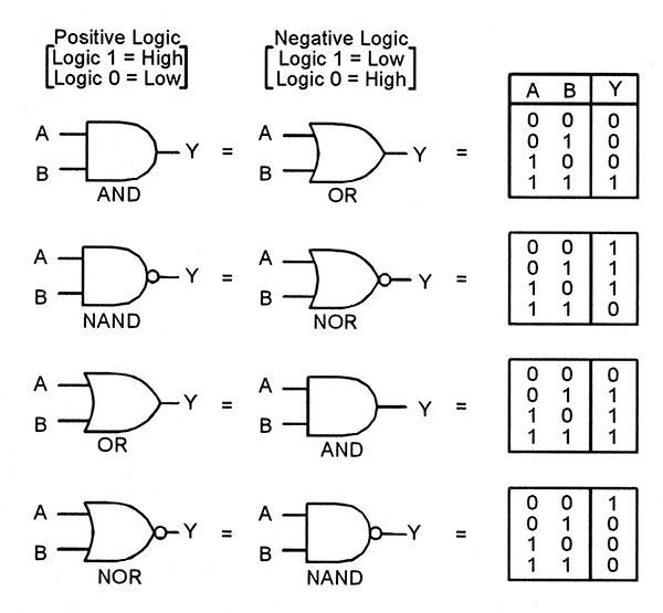
FIGURE 4. Basic sets of two-input positive and negative logic equivalents.
Thus, it can be seen that a negative logic AND gate action — in which the output is low only when both inputs are low — is directly available from a positive logic OR gate, and so on.
Practical Buffer IC Circuits
Digital buffer ICs have two main purposes: to act either as simple non-inverting, current-boosting interfaces between one part of a circuit and another, or to act as three-state switching units that can be used to connect a circuit’s outputs to a load, only when required. If you ever need only a few simple buffers, one cheap way to get them is to make them from spare AND or OR elements (as shown in Figure 5) or from pairs of normal or Schmitt inverters (as shown in Figure 6).

FIGURE 5. Any AND or OR gate can be used as a non-inverting buffer element.
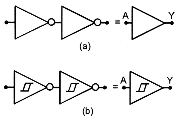
FIGURE 6. Any two elements from an inverter IC can be used to make a non-inverting buffer element.
Figure 7 lists basic details of nine popular, non-inverting digital buffer ICs.

FIGURE 7. Nine popular non-inverting buffer ICs.
When using these ICs, note that all unused buffers must be disabled by tying their inputs to one of the IC’s supply lines. In CMOS devices, the unused inputs can be tied directly to either supply line, but in TTL devices, it is best (for lowest quiescent current consumption) to tie all unused inputs high via a common 10K resistor. If the unused buffer is a three-state type, it should (if it has independent control) be set into its normal mode via its control input.
Dealing now with the individual buffer ICs listed in Figure 7, Figure 8 shows the functional diagram and truth table, etc., of the 74LS125 TTL IC, which houses four independently controlled, three-state buffers and is so modestly priced that it is still worth using, even if you do not need the three-state facility.
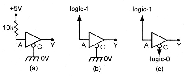
FIGURE 8. Functional diagram and truth table, etc., of the 74LS125 Quad three-state buffer/bus-driver IC.
Note from the truth table that each of the four elements acts as a normal buffer when its control terminal (C) is in the logic 0 state, and that the element’s quiescent current (Is) is least when C is at logic 0 and the buffer’s input (A) is at logic 1.
Thus, any unwanted elements should be disabled by tying their C terminals low and their A terminals high, using one of the methods shown in Figure 9.
FIGURE 9. All unwanted 74LS125 elements must be connected in one of these ways.
Any element can be used as a normal buffer by grounding its C terminal (Figure 10), or as a three-state buffer that drives a common bus line by using it as shown in Figure 11.
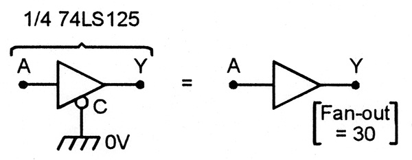
FIGURE 10. Methods of using a 74LS125 element as a normal buffer.
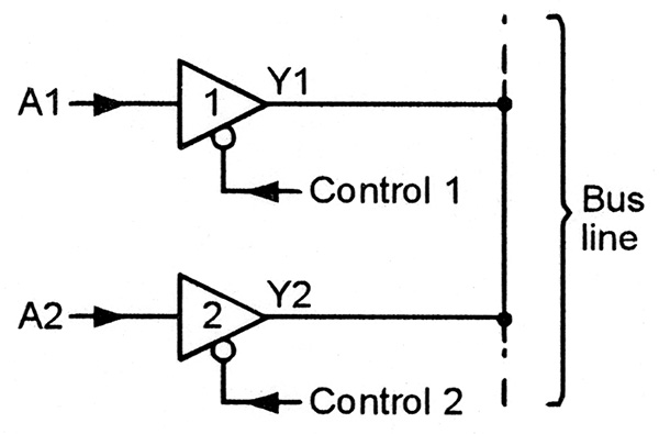
FIGURE 11. Methods of using a 74LS125 element as a three-state line-driving buffer.
If you need up to six simple CMOS buffers, one of the cheapest ways to get them is via a 4050B or 74HC4050 Hex buffer IC. Figure 12 shows the IC’s functional diagram; each buffer can source up to 10 mA or sink up to 40 mA of output current when the IC is powered from a 15V supply.
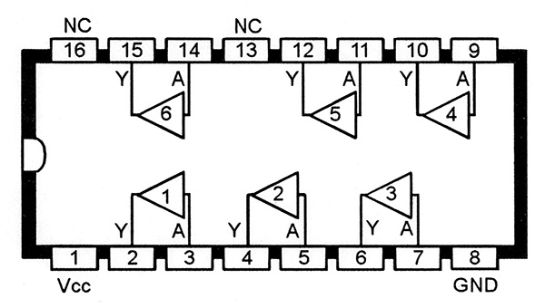
FIGURE 12. Functional diagram of the 4050B or 74HC4050 Hex buffer IC.
If you need up to six three-state CMOS buffers, one option is to use a 4503B Hex buffer IC. Figure 13 shows the functional diagram and truth table of this versatile IC, in which pin 1 acts as a DISABLE input that controls four of the six buffers, and pin 15 acts as a DISABLE input that controls the other two buffers.
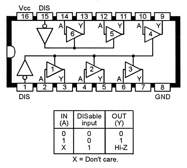
FIGURE 13. Functional diagram and truth table of the 4503B Hex buffer IC.
Note that each buffer element acts as a normal buffer when its DISABLE pin is at logic 0 (low), and goes into the high-impedance output state when its DISABLE pin is at logic 1 (high).
Thus, this IC can be used as a simple Hex buffer by wiring it as shown in Figure 14 (with pins 1 and 15 grounded), or as a Hex three-state buffer that is controlled via a single input by wiring it as shown in Figure 15 (with pins 1 and 15 shorted together and used as a DISABLE input).
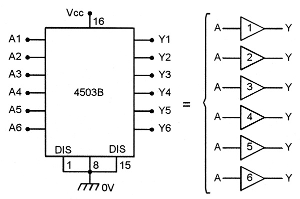
FIGURE 14. Method of connecting the 4503B for use as six normal buffers.
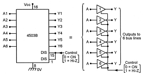
FIGURE 15. Method of connecting the 4503B for use as a three-state Hex buffer controlled via a single input.
Figure 16 shows the functional diagram of the 7407, which is a standard TTL Hex buffer in which each buffer has an open-collector output that can sink up to 40 mA and can be connected to a supply of up to 30V via an external current-limiting pull-up resistor (but the actual IC must use a 5V supply).
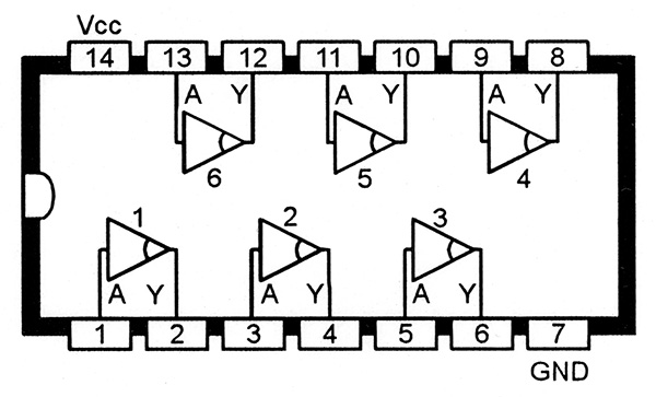
FIGURE 16. Functional diagram of the 7407 Hex buffer with 30V o.c. outputs.
Figure 17 shows how one of these buffers can be used as a 5V to high-voltage (up to 30V) non-inverting interface.
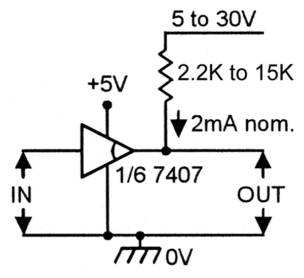
FIGURE 17. A 5V to high-voltage buffer/interface.
Figure 18 shows how three o.c. buffers can be made to act as a wired AND gate by wiring all three outputs to the same pull-up resistor.

FIGURE 18. Three 7407 buffers used to make a three-input wired AND gate.
The circuit action is such that the output is pulled low when any input is low, and only goes high when all three inputs are high, thus giving an AND action.
Figure 19 shows the functional diagram and basic truth table of a 74LS365 Hex three-state buffer IC, in which all six buffers share a common AND-gated control line.
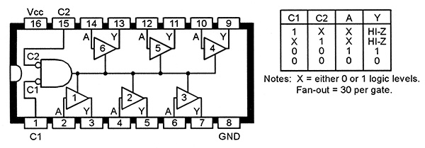
FIGURE 19. Functional diagram and truth table of the 74LS365 Hex three-state buffer.
This IC can be used as six normal buffers by grounding its two control pins as shown in Figure 20, or as a set of six three-state buffers that are all switched via one common control signal as shown in Figure 21; AND-type three-state control can be obtained by using both Control terminals (pins 1 and 15).

FIGURE 20. Methods of connecting the 74LS365 for use as six normal buffers.
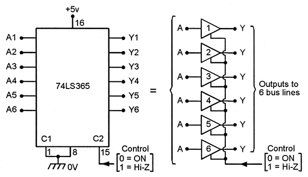
FIGURE 21. Methods of connecting the 74LS365 for use as a three-state Hex buffer controlled via a single input.
Finally, the 74HC241, 74HC244, and 74LS244 are ‘Octal’ three-state Schmitt buffers in which the buffers are split into two groups of four, with the mode of each group controlled via a separate input. Figure 22 shows the functional diagram and truth table of the 74LS244 IC (the 74HC244 is similar, but it has Schmitt-type CA and CB inputs).
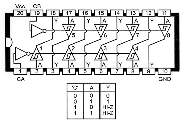
FIGURE 22. Functional diagram and truth table of the 74LS244 (or 74HC244) Octal (dual Quad) three-state Schmitt buffer IC.
The IC is really a dual Quad device, in which buffers 1-4 are controlled via the CA terminal, and buffers 5-8 are controlled via the CB terminals.
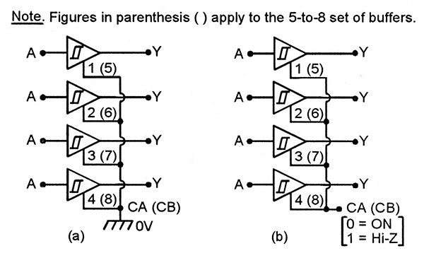
FIGURE 23. The 74LS244 Quad buffers can be used as (a) simple Schmitt buffers, or as (b) three-state ganged Schmitt buffers.
Each of these Quads can be used as a set of simple Schmitt buffers by grounding its control terminal as shown in Figure 23(a), or as a ganged set of three-state Schmitt buffers by using its control terminal as shown in Figure 23(b). NV