In our last episode, we explained modern TTL and CMOS logic gate basics and gave practical descriptions of some of the most popular digital buffer ICs that are available. This time, we'll expand on this basic theme and take detailed looks at some popular digital inverter and AND gate ICs.
As you read through this, note that some of the ICs mentioned may not be available via your local supplier, but should still be available from specialist dealers.
Practical Digital Inverter Circuits
The digital inverter (or NOT gate) is the most basic of all digital logic elements, and is sometimes called an inverting buffer. If you ever need only a few simple inverters, one cheap way to get them is to make them from spare TTL or CMOS NAND or NOR elements, connected in the basic way shown in Figure 1, in which the input terminals of a two input NAND or NOR gate are shorted together to accept a single input and give a single (but inverted) output signal.
FIGURE 1. Any NAND or NOR gate can be used as an inverting buffer element.
Figure 2 lists basic details of some popular digital inverter ICs.
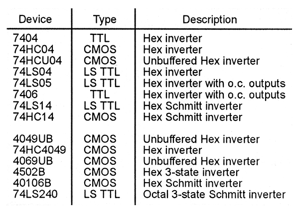
FIGURE 2. Fourteen popular inverter ICs.
When using these ICs, note that all unused inverters must be disabled by tying their inputs to one of the IC’s low voltage supply lines. In CMOS devices, the unused inputs can be tied directly to either supply line, but in TTL devices, it is best (for lowest quiescent current consumption) to tie all unused inputs directly to the 0V rail. If the unused inverter is a three-state type, it should (if it has independent controls) be set into its normal mode via its control input, to minimize current drain.
Dealing now with the individual inverter ICs listed in Figure 2, Figure 3 shows the functional diagram that is common to the popular 7404, 74LS04, 74HC04, 74HCU04, and 4069UB Hex inverter ICs.
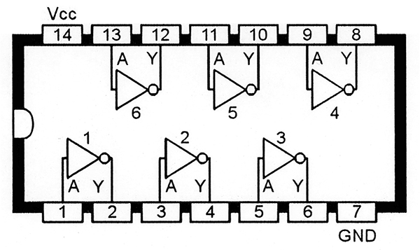
FIGURE 3. Functional diagram of the 7404, 74LS04, 74HC04, 74HCU04, or 4069UB Hex inverter ICs.
Of these, the 7404 is an ancient standard TTL IC; the 74LS04 is a modern LS TTL type in which each inverter has a fan-out of 10, the 74HC04 is a fast CMOS type, and the 74HCU04 and 4069UB are unbuffered CMOS types that are suitable for use in linear applications.
Figure 4 shows the functional diagram that is common to the 74LS05 and 7406 Hex inverters with open collector (OC) outputs.
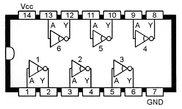
FIGURE 4. Functional diagram of the 74LS05 or 7406 Hex inverters with open collector outputs.
The 74LS05’s OC outputs can handle maximum outputs of only 5.5 volts, but those of the 7406 can handle up to a maximum of 30 volts.
Figure 5 shows the functional diagram that is common to three of the most useful of all Hex inverter ICs — the 74LS14 TTL and the 74HC14 and 40106B CMOS Schmitt types.

FIGURE 5. Functional diagram of the 74LS14, 74HC14, or 40106B Hex Schmitt inverter ICs.
In the 74LS14, the output of each Schmitt inverter is in the logic 1 state until the input rises to an upper threshold value of 1.6V, at which point the output switches to logic 0 and locks there until the input is reduced to a lower threshold value of 0.8V. At this point, the output switches and locks into the logic 1 state again, and so on. Thus, a 74LS14 Schmitt inverter can be made to function as a sine-to-square converter by connecting it as shown in Figure 6, where RV1 is used to set the circuit to its maximum sensitivity point, at which a quiescent voltage of 1.2V is set on the inverter’s input.

FIGURE 6. A TTL Schmitt inverter sine-to-square converter.
Figures 7 through 9 show more simple applications of the 74LS14 IC. Figure 7 is a practical version of a mechanical-switch contact-bounce debouncer; it can be activated by a push-button (S1) or toggle (S2) switch, and has an output that goes to logic 1 when the switch is closed.
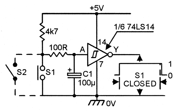
FIGURE 7. TTL switch debouncer, with logic 1 closed output.
Figure 8 is a modified version of the above circuit, with an added inverter stage, and gives a logic 0 output when S1 is closed.
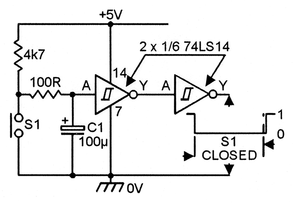
FIGURE 8. TTL switch debouncer, with logic 0 closed output.
Figure 9 is yet another variation of the basic circuit, and generates a brief logic 1 switch-on output pulse when the circuit’s supply is first connected.

FIGURE 9. TTL supply switch-on pulse generator.
Regarding the 74HC14 and 40106B CMOS Schmitt inverters, these have typical upper and lower threshold voltage values equal to 60% and 40% of the supply voltage respectively. A CMOS Schmitt inverter can thus be made to function as a sine-to-square converter by connecting it as shown in Figure 10, where RV1 is used to set the circuit to its maximum sensitivity point.
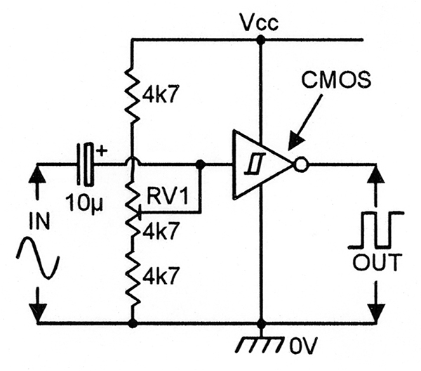
FIGURE 10. CMOS Schmitt inverter sine/square converter.
Alternatively, either CMOS Schmitt inverter can be used as a switch-on pulse generator (which generates a brief logic 1 switch-on output pulse when the circuit’s supply is first connected) by wiring it as shown in Figure 11.
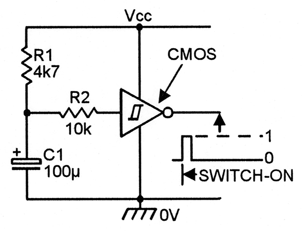
FIGURE 11. CMOS supply switch-on pulse generator.
Note in this circuit that resistor R2 is used to give the CMOS IC element a reasonable degree of protection against damage from excessive C1 discharge current if a short circuit suddenly appears acoss the circuit’s two supply lines.
Figure 12 shows the functional diagram that is common to the 4049UB and 74HC4049 Hex CMOS inverter ICs.

FIGURE 12. Functional diagram of the 4049UB (unbuffered) or 74HC4049 (buffered) Hex inverter IC.
The 4049UB is an unbuffered type, suitable for use in linear applications, and the 74HC4049 is a fast, fully buffered general-purpose device.
Figure 13 shows the functional diagram and truth table of the 4502B.
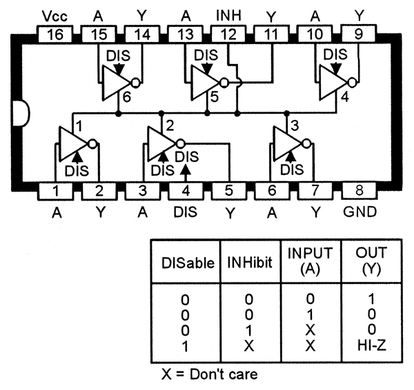
FIGURE 13. Functional diagram and truth table of the 4502B Hex three-state inverter with INHIBIT control.
This is a special-purpose, three-state Hex inverter in which the outputs of all six inverters can be set to the logic 0 state by driving the INHIBIT (pin 12) terminal high, or can be set to the high-impedance state by driving the DISABLE (pin 4) terminal high. The IC can be used as a conventional Hex inverter by grounding the INHIBIT and DISABLE pins, or as a normal three-state inverter by grounding the INHIBIT pin and applying the three-state control to the DISABLE terminal.
Finally, Figure 14 shows the functional diagram and truth table of the 74LS240 octal three-state Schmitt inverting buffer IC, in which each buffer has a fan-out of 30.
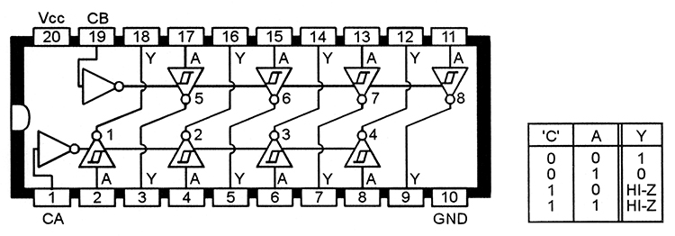
FIGURE 14. Functional diagram and truth table of the 74LS240 octal (dual quad) three-state Schmitt inverting buffer IC.
This IC is actually a dual quad device, in which inverters 1-4 are controlled via the CA terminal, and inverters 5-8 are controlled via the CB terminal. Each of these quads can be used as a set of normal Schmitt inverters by grounding the control terminal, or as a ganged set of three-state Schmitt inverters by using its control terminals as shown in the truth table.
Practical AND-Gate IC Circuits
The output of an AND gate goes high (to logic 1) when all of its inputs (A, B, and C, etc.) are high. Figure 15 lists basic details of several popular AND-gate ICs.
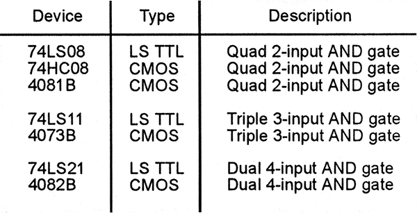
FIGURE 15. Seven popular AND gate ICs.
Of these, the 74LS08, 74HC08, and 4081B (see Figures 16 and 17) are quad two input types.
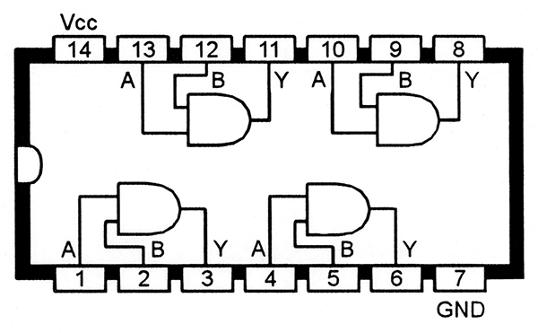
FIGURE 16. Functional diagram of the 74LS08 or 74HC08 quad two-input AND gate ICs.
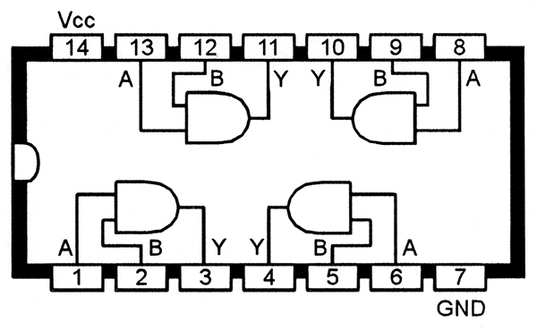
FIGURE 17. Functional diagram of the 4081B quad two-input AND gate IC.
The 74LS11 and 4073B (see Figures 18 and 19) are triple three-input types.
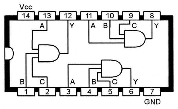
FIGURE 18. Functional diagram of the 74LS11 triple three-input AND gate IC.

FIGURE 19. Functional diagram of the 4073B triple three-input AND gate IC.
The 74LS21 and 4082B (see Figures 20 and 21) are dual four input types.
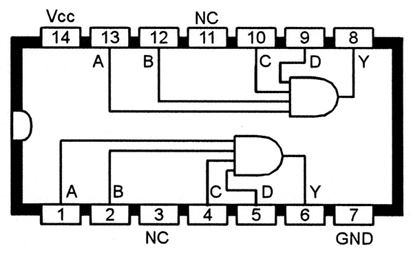
FIGURE 20. Functional diagram of the 74LS21 dual four-input AND gate IC.
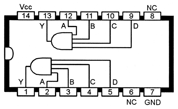
FIGURE 21. Functional diagram of the 4082B dual four-input AND gate IC.
When using AND-gate ICs, each unwanted gate must be disabled by shorting all of its inputs together and tying them to one of the IC’s supply lines. In CMOS ICs, the shorted inputs can be wired directly to either supply line, but in TTL ICs the inputs must (to give minimum quiescent current consumption with good stability) be tied to the positive supply rail via a single 1K resistor, as shown in Figure 22.
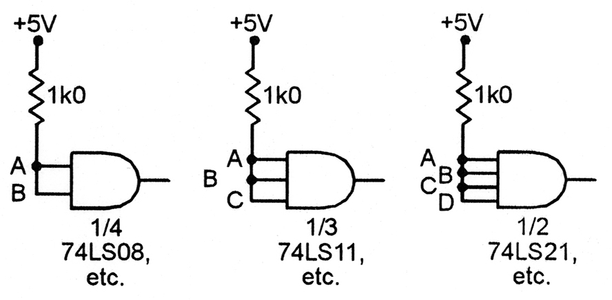
FIGURE 22. Method of disabling unwanted TTL AND gates.
A single resistor can be used as a tie point for large numbers of unwanted inputs.
Sometimes, when using three or four input AND gate ICs, you may not want to use all of a gate’s input terminals. In this case, the unwanted inputs can be disabled by either tying them high (directly in CMOS gates, or via a 1K resistor in TTL types) or by simply shorting them directly to a used input. Figure 23 shows examples of three input and four input TTL AND gates wired for use as two input types.
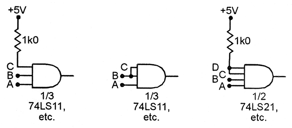
FIGURE 23. Methods of disabling unwanted TTL inputs, to make a two-input AND gate.
Note that the fan-in of a TTL AND gate is an almost constant 1, irrespective of the number of inputs used. Thus, CMOS or TTL AND gates can be converted into non-inverting buffers by simply shorting all of their inputs together. Figure 24 shows examples of TTL AND gates used as simple buffers.
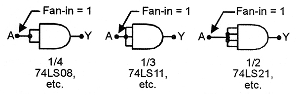
FIGURE 24. Methods of using TTL AND gates as simple buffers.
A useful feature of AND gate ICs is that their gates can be directly cascaded, with the output of one gate feeding directly into one input of another gate, to make compound AND gates with any desired number of inputs. Figure 25, for example, shows how two input AND gates can be cascaded to make three, four, or five input AND gates.

FIGURE 25. Ways of using two input AND gates to make (a) three input, (b) four input, or (c) five input AND gates.

FIGURE 26. Ways of using (a) three input or (b) four input AND gates to make a seven input AND gate.
Figure 26 shows three three input or two four input gates cascaded to make a single seven input AND gate. NV