One of the most important events in the history of digital electronics was the development of the new IC technology known as CMOS in 1969. CMOS (Complementary-symmetry MOSFET) digital IC elements have major advantages over TTL types. They are simple and inexpensive, consume near-zero quiescent current, have a very high input impedance, can operate over a wide range of supply voltages, have excellent noise immunity, and are very easy to use.
In 1972, practical CMOS arrived on the commercial scene in the form of a brand-new medium-speed family of digital ICs known as the ’4000’-series. This new family was not as fast as the TTL technology then in use in the rival ‘74’-series of digital ICs, but in the mid 1980s, a new high-speed type of CMOS was developed and introduced as a new member of the 74 family of devices. The advantages of this new ‘fast’ CMOS were so great that in 1994, it overtook TTL in popularity within the 74-series, finally making CMOS the most popular of all modern digital IC technologies.
This final episode explains the operating principles of these 4000- and 74-series CMOS devices, and describes CMOS basic usage rules.
CMOS Basics
The most basic element in any digital IC family is the digital inverter. Figure 1 (repeated from Part 1 of this four-part series) shows a basic CMOS inverter.
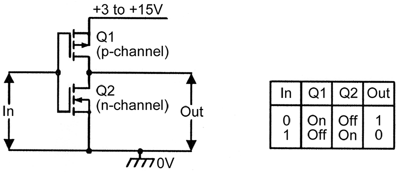
FIGURE 1. Circuit and Truth Table of a basic CMOS inverter.
It is a ‘totem-pole’ type of amplifier and consists of a complementary pair of enhancement-mode MOSFETs wired in series between the two supply lines, with p-channel MOSFET Q1 at the top and n-channel MOSFET Q2 below and with the MOSFET gates (which have a near-infinite DC input impedance) tied together at the input terminal and the output taken from the junction of the two devices. The pair can be powered from any supply in the 3V to 15V range. The basic digital action of the n-channel device is such that its drain-to-source path acts like an open-circuit switch when the input is at logic-0, or as a closed switch in series with a 400Ω resistor when the input is at logic-1. The p-channel MOSFET has the inverse of these characteristics, and acts like a closed switch plus a 400Ω resistance with a logic-0 input, and an open switch with a logic-1 input. The basic action of the CMOS inverter can be understood with the help of Figure 2.
FIGURE 2. Equivalent circuit of the CMOS digital inverter with (a) logic-0 and (b) logic-1 inputs.
Figure 2(a) shows the digital equivalent of the CMOS inverter circuit with a logic-0 input. Under this condition, Q1 (the p-channel MOSFET) acts like a closed switch in series with 400Ω, and Q2 acts like an open switch. The circuit thus draws zero quiescent current but can ‘source’ fairly large drive currents into an external output-to-ground load via the 400Ω output resistance (R1) of the inverter. Figure 2(b) shows the inverter’s equivalent circuit with a logic-1 input. In this case, Q1 acts like an open switch, but Q2 (the n-channel MOSFET) acts like a closed switch in series with 400Ω; the inverter thus draws zero quiescent current under this condition, but can ‘sink’ fairly large currents from an external supply-to-output load via its internal 400Ω output resistance (R2).
Thus, the basic CMOS digital inverter can be used with any supply in the 3V to 15V range, has a near-infinite input impedance, draws near-zero (typically 0.01 µA) supply current with a logic-0 or logic-1 input, can source or sink substantial output currents, and has an output impedance of about 400W. Note that, unlike the TTL inverter, its output can swing all the way from zero to the full positive supply rail value, since no potentials are lost via saturation or forward-biased junction voltages, etc. Typically, a basic (mid 1970s style) CMOS stage has a propagation delay ranging from 12 ns when using a 12V supply, to 60 nS at 3V, etc.
The ‘4000A’-Series of ICs
The initial 1972 range of digital ICs was known as the ‘4000A’ series; it used the basic type of CMOS inverter shown in Figure 1, but incorporated extensive diode-resistor ‘clamping’ networks to protect its MOSFETs against damage from static charges, etc. Thus, a complete A-series inverter stage took the basic form shown in Figure 3.
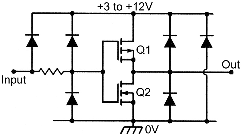
FIGURE 3. Basic 4000A-series inverter stage, with internal input and output protection networks.
Commercial testing of the early A-series range of CMOS devices quickly revealed a number of design problems. Their on-off resistance values were, for example, very sensitive to gamma radiation effects, thus limiting their value in outer-space projects, and they gave uneven ‘high’ and ‘low’ output impedances and propagation delays, etc. (i .e., they had poor output symmetry). But the most important problem was that their output switching levels were overly sensitive to the magnitudes of their input switching signals; the root cause of this problem can be understood with the aid of Figure 4, which shows the linear characteristics of the CMOS inverter’s two MOSFETs when they are operated from a 15 volt supply.
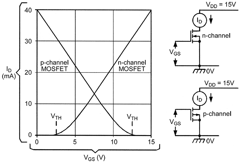
FIGURE 4. Typical gate-volts/drain-current characteristics of p- and n-channel MOSFETs operating from a 15V supply.
Note in Figure 4 that each MOSFET acts like a voltage-controlled resistance. The n-channel device has a near-infine drain-to-source resistance at zero input voltage: the resistance remains high until the input rises to a ‘threshold’ value of about 1.5 to 2.5 volts, but then decreases as the input voltage is increased, eventually falling to about 400Ω when the input equals the supply line voltage. The p-channel MOSFET has the reverse of these characteristics. Thus, when the two MOSFETs are wired in series and used as a 15 volt basic CMOS inverter, they produce the typical drain-current transfer graph shown in Figure 5, and the voltage transfer graph of Figure 6; these graphs can be explained as follows.
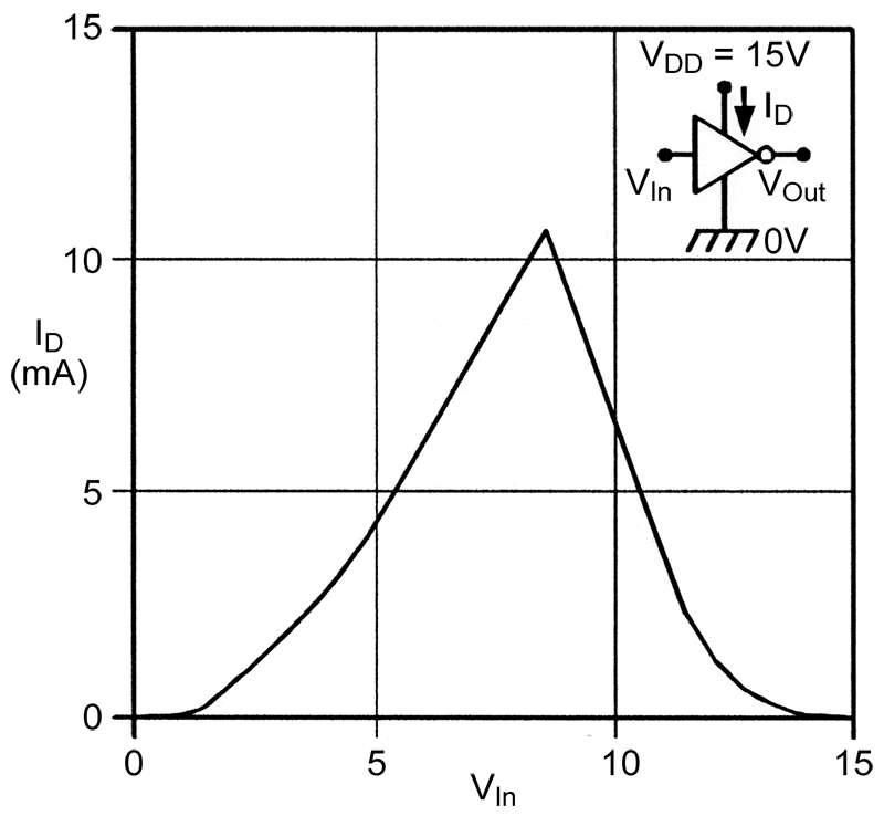
FIGURE 5. Typical drain-current transfer characteristics of the simple CMOS inverter.
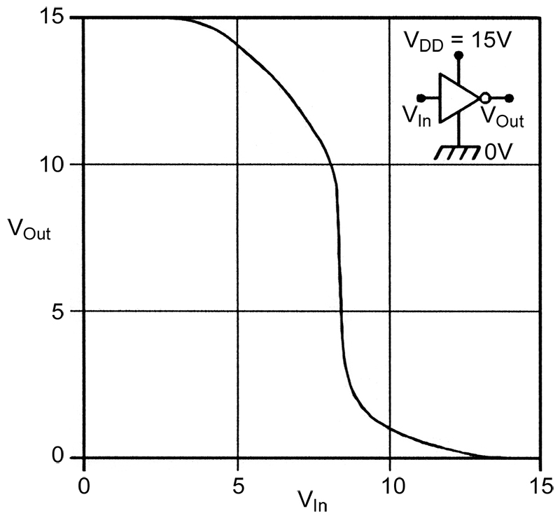
FIGURE 6. Typical voltage transfer characteristics of the simple CMOS inverter.
Suppose in Figures 5 and 6 that the CMOS inverter’s input voltage is slowly increased upwards from zero. The inverter current is near zero until the input exceeds the n-channel MOSFET’s threshold voltage, at which point its resistance starts to fall and that of the p-channel MOSFET starts to increase. Under this condition, the inverter current is dictated by the larger of the two resistances; when the input is far less than half-supply volts, the n-channel MOSFET resistance is far greater than that of the p-channel device, so the output is high (at logic-1).
When the input is at a transition value somewhere between 30 and 70 percent of the supply voltage, the two MOSFETs have similar resistance values and the inverter acts as a linear amplifier with a voltage gain of about 30 dB and draws several milliamps of supply current. Under this condition, small changes of input voltage cause large changes of output voltage. When the input is further increased — well above half-supply volts — the resistance of the n-channel MOSFET falls below that of the p-channel device, and the output goes low (to logic-0). Finally, when the input rises above the threshold value of the p-channel MOSFET, it acts like an open switch, and the inverter current again falls to near zero.
Thus, the A-series type of inverter gives an output that switches fully between the supply rail values only if its input voltage swings well above and below its two internal threshold voltage values. Note (from Figure 5) that the CMOS draws a brief pulse of supply current each time it goes through a switching transition; the more often CMOS changes state in a given time, the greater are the number of current pulses that it takes from the supply and the greater is its mean current consumption. Thus, CMOS current consumption is directly proportional to switching frequency.
The ‘4000B’-Series of ICs
The defects of the 4000A-series were so severe that an improved CMOS series, known as the ‘4000B’ or buffered series, was introduced around 1975, and the old 4000A-series was slowly phased out of production. The major feature of this new series is that each of its ‘inverters’ consists of three basic inverters wired in series, as shown in Figure 7, so that each ‘buffered’ inverter has a typical linear voltage gain of 70 to 90 dB and has the typical voltage transfer graph of Figure 8, in which any input below VDD/3 is recognized as a logic-0 input and any input above 2VDD/3 is recognized as a logic-1 input.
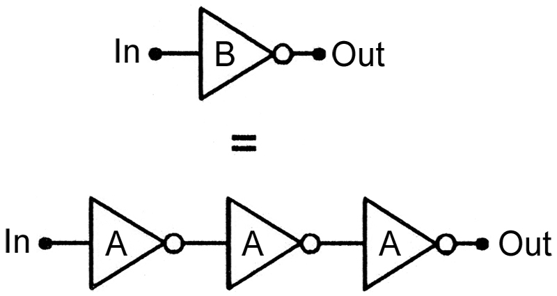
FIGURE 7. A B-series CMOS inverter can be made by wiring three A-series types in series.
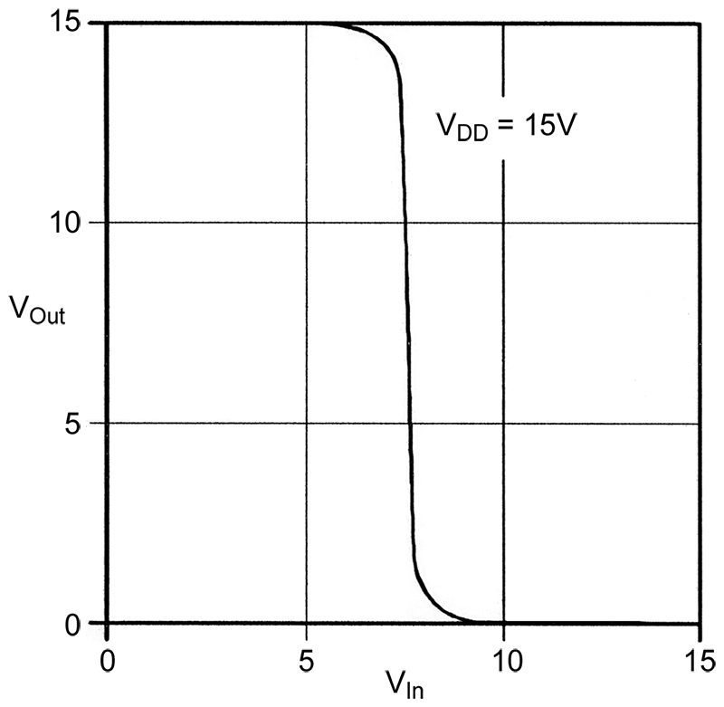
FIGURE 8. Voltage transfer graph of the Figure 7 B-series inverter.
Other changes in the new series include greatly improved output-drive symmetry and immunity to gamma-radiation effects, new and better input and output protection networks (see Figure 9), and improved voltage ratings (usually to 15V maximum, but to 18V maximum in some manufacturer’s versions, compared to 12V maximum in the original A-series).
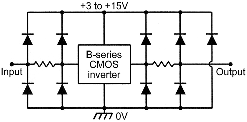
FIGURE 9. Basic 4000B-series inverter with typical input and output protection networks.
One disadvantage of the B-series is that its propagation delays are larger than those of the old A-series. To counter this problem, a few new-generation devices are produced in an ‘unbuffered’ format (denoted by a ‘UB’ suffix), but incorporate all the other improvements of the B-series.
Typically, UB inverters have an AC gain of 23 dB at 10 volts, and are useful in several analog applications. Note that the bandwidth and propagation delays of a CMOS device vary with supply voltage and with capacitive output loading. Figure 10 lists the typical propagation delays of both UB and B-series inverters when used with supply values of 5V, 10V, and 15V when driving a 50 pF load.
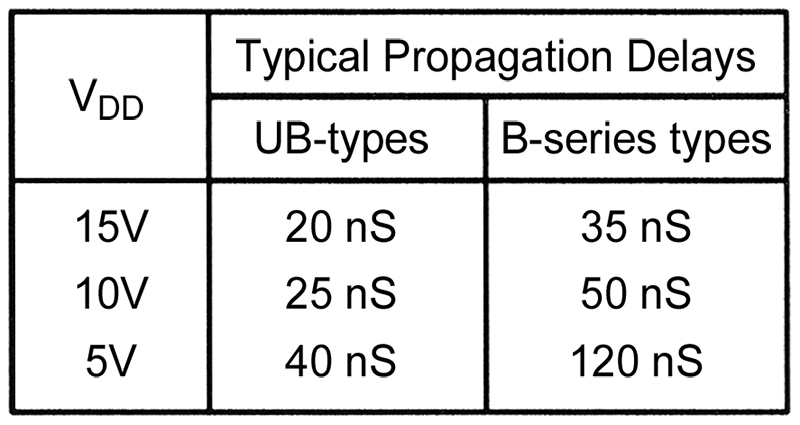
FIGURE 10. Typical propagation delays of 4000B-series inverters when driving a 50 pF load.
The ‘4500B’-Series of ICs
The 4000B-series range of ICs consists mainly of fairly simple SSI or MSI devices such as logic gates and simple counters, etc. In the late 1970s and early 1980s, a number of more complex MSI and LSI B-type CMOS ICs such as encoders, decoders, and presettable counters (etc.), were introduced. These advanced devices carry ‘45XX’ or ‘47XX’ numbers, and are generally known as the 4500-series of CMOS ICs.
‘Fast’ CMOS ICs
In the early 1980s, engineers strove to design a really fast type of CMOS that could outclass LS TTL when operated from a five-volt supply and could thus become the dominant technology within the 74 series of ICs. Normal CMOS is based on MOSFET (Metal-Oxide Silicon FET) technology, and this is simply a variation of IGFET (Insulated-Gate FET) technology. Specifically, a MOSFET device is an IGFET device that uses metal-oxode gate insulation, and the first big step in developing ‘fast’ CMOS was to use silicon-oxide rather than metal-oxide gate insulation in the basic IGFETs.
This simple measure resulted in a dramatic reduction in the IGFET’s internal input capacitance and an equally dramatic increase in operating speed. The next step was to apply these new IGFETs to the basic CMOS configuration. When this was done and significant changes were made in the element’s geometry, the resulting device acted like normal CMOS but was as fast as LS TTL when operated from a five-volt supply and (unlike some other versions of CMOS) had excellent output drive capability. Strictly, this new device should have been given a special name such as CSOS (Complementary Silicon-Oxide Silicon FET), but instead was simply christened ‘fast’ CMOS.
Fast CMOS has many similarities with conventional 4000B-series CMOS. It is available in both buffered (triple-inverter) and unbuffered (single inverter) basic versions, and has all inputs and outputs protected via internal diode-resistor networks. It can (in most cases) use any supply in the 2V to 6V range, and when first introduced, was intended to replace many existing devices in the 74 series of ICs. Since then, however, it has also been used to make fast versions of many popular devices within the 4000B and 4500B series of ICs.
CMOS 74-Series Sub-Families
When the 74-series of IC first appeared in 1972, it was based entirely on TTL technology, which inherently consumes a fairly high quiescent current. In the late 1970s, a slightly modified version of standard CMOS (optimized for 5V operation) was introduced as a new ‘C’ sub-family within the 74-series range of devices, and offered the advantage of near-zero quiescent current consumption. This C sub-family was too slow and had too weak an output-drive capability to obtain great popularity, but in later years, the fast type of CMOS was developed specifically for use in the 74-series, as already described, and so far a total of five CMOS sub-families have been introduced in the 74-series, as follows:
- Standard (C) CMOS (now obsolete). This was virtually normal MOSFET-type CMOS in a 74-series format. Typically, a single 74C00 two-input NAND gate consumed about 15 mW at 10 MHz, and had a propagation delay of 60 nS at 5V.
- High-speed (HC) CMOS. Introduced in the early 1980s, this is the basic fast silicon-oxide version of CMOS, and gives speed performances similar to LS TTL, but with CMOS levels of power consumption. HC 74-series devices using this technology have CMOS-compatible inputs. Typically, a single 74HC00 two-input NAND gate consumes less than 1 µA of quiescent current, and has a propagation delay of 8 nS at 5V.
- High-speed (HCT) CMOS. These are fast HC-type devices, but have TTL-compatible inputs and are meant to be driven directly from TTL outputs. Typically, a 74HCT00 two-input NAND gate consumes less than 1 µA of quiescent current and has a propagation delay of 18 nS.
- Advanced high-speed (AC) CMOS. In the late 1980s, further advances in high-speed CMOS design and fabrication techniques yielded even better speed performances. AC 74-series devices using this technology have CMOS-compatible inputs. Typically, a 74AC00 two-input NAND gate has a propagation delay of 5 nS.
- Advanced high-speed (ACT) CMOS. These are AC-type devices, but have TTL-compatible inputs and are meant to be driven from TTL outputs. Typically, a 74ACT00 two-input NAND gate has a propagation delay of 7 nS.
Basic CMOS Circuit Variations
There are three important variations of the basic CMOS circuit that are often used in ICs in the medium-speed 4000B-series and fast 74-series ranges of devices. The first of these is the ‘open drain’ configuration, which is used in some inverters and buffers, etc. Figure 11 shows a typical open-drain inverter, which is configured like a normal high-gain three-stage CMOS inverter except that the final stage consists of a single n-channel enhancement-mode IGFET (Q1) that has its drain connected directly to the circuit’s output terminal.
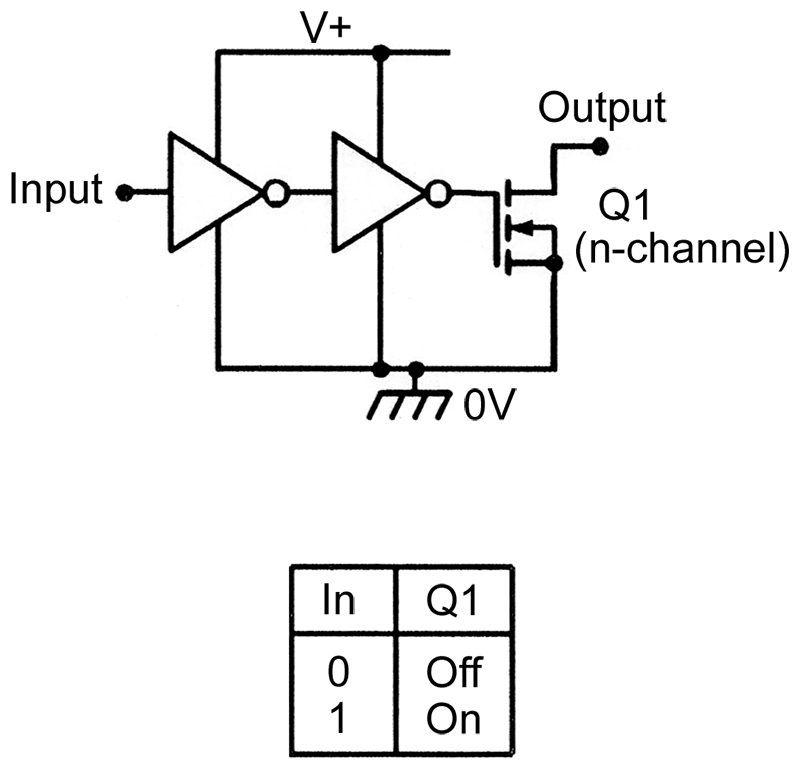
FIGURE 11. Basic CMOS inverter with open-drain output.
The circuit’s action is such that Q1 is cut off when the input is at logic-0, and is driven on when the input is at logic-1. The circuit can be used to directly drive an external load that is connected between ‘OUT’ and the +ve supply rail, in which case the load activates when a logic-1 input is applied.
The second variation concerns the use of a ‘three-state’ type of output that in normal use gives a conventional logic-0 or logic-1 low-impedance output, but can also be set to a third state in which the output is effectively open-circuit. This facility is useful in allowing several outputs or inputs to be wired to a common bus and to communicate along that bus by ENABLING only one output and one input device at a time.
Figure 12 shows the typical circuit of a non-inverting buffer of this type, together with its truth table.
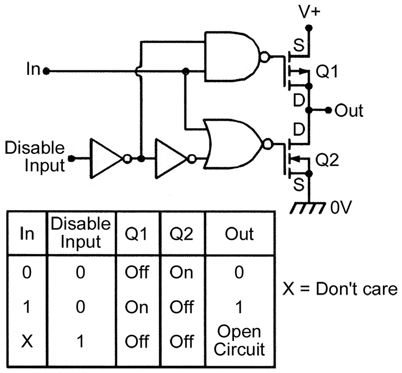
FIGURE 12. Basic circuit of a three-state CMOS non-inverting buffer.
Thus, when the DISABLE INPUT control is at logic-0, the circuit gives normal ‘buffer’ operation; under this condition, Q1 is driven OFF and Q2 is driven ON when IN is at logic-0, thus driving OUT to logic-0. The reverse of this action is obtained when the input is at logic-1. When the DISABLE INPUT control is set to logic-1, both Q1 and Q2 are driven OFF, irrespective of the state of the IN input, and under this condition, OUT is effectively disabled, and acts as an open circuit. Figure 13 shows the simplified equivalent circuit of this buffer when it is in its high-impedance output state.
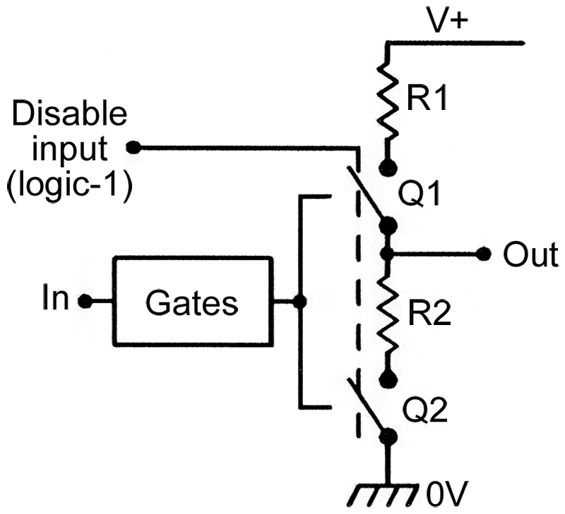
FIGURE 13. Equivalent of a three-state buffer circuit in its third high-impedance state.
The third CMOS circuit variation is that of the ‘bilateral switch’ or transmission gate. The basic action of any enhancement-mode IGFET is such that its drain-to-source path acts like a near-perfect unidirectional switch: When the IGFET is OFF, the path acts like an open circuit, and when it is ON, it acts like a low-value resistor and (unlike a bipolar transistor) does not suffer from saturation-voltage problems, etc. When turned on, an n-channel IGFET passes current from drain-to-source, and a p-channel IGFET passes current from source-to-drain. Thus, a near-perfect bidirectional or bilateral electronic switch can be made by wiring an n-channel and a p-channel IGFET in parallel (source-to-source and drain-to-drain) and driving their gates in anti-phase, as shown in Figure 14.
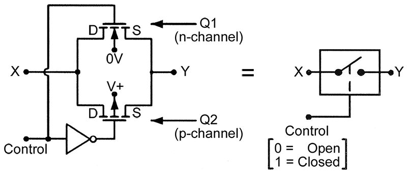
FIGURE 14. Basic CMOS bilateral switch or transmission gate.
Here, both IGFET paths are effectively open when the CONTROL input is at logic-0, and closed when the CONTROL input is at logic-1. Under the closed condition, current can flow from X to Y via Q1, or from Y to X via Q2; current can thus flow in either direction between these points, and the circuit thus simulates a simple electro-mechanical switch.
CMOS Basic Usage Rules
CMOS ICs are very easy to use. They are very tolerant of supply voltage variations and, unlike TTL types, present very few input-drive/output-drive matching problems. There are, in fact, only seven basic usage themes to consider when dealing with CMOS which are: Type selection; Handling CMOS; Power supplies; Input signals; Unused inputs; and Interfacing.
Type Selection
The question “Which CMOS family should I use?” can easily be answered with the help of Figure 15, which lists the major characteristics of the six readily-available modern CMOS sub-families and compares them with those of LS TTL. Of these types, the 4000UB sub-family is only available in the form of a few simple buffer and inverter ICs, and should be regarded as a simple variant of the main 4000B sub-family. The 74HCT and 74ACT types are meant to be directly driven from TTL outputs, and are of use only in a few specialized applications.
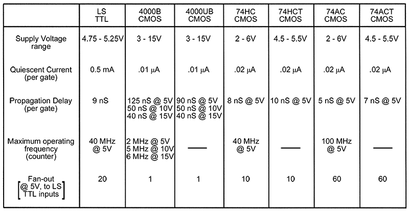
FIGURE 15. Table showing general characteristics of LS TTL and the six major CMOS digital IC types.
Of the remaining three CMOS sub-families (4000B, 74HC, and 74AC), the 4000B sub-family can be used in any application that requires the use of a supply in the range of 3V to 15V and in which maximum operating frequencies do not exceed 2 MHz at 5V, or 6 MHz at 15V. Alternatively, if supply voltages are restricted to the 2V to 6V range, the 74HC sub-family can be used to operate at frequencies up to 40 MHz at 5V, or the 74AC sub-family at frequencies up to 100 MHz at 5V.
Note that all TTL ICs have special input-drive requirements, and the fan-out numbers in Figure 15 show how many parallel-connected standard LS TTL inputs can be directly driven from the output of each listed sub-family member. Thus, 4000B CMOS can only drive one such input, but 74HC and HCT CMOS can each drive 10 such inputs, and 74AC and ACT can each drive up to 60 LS TTL inputs.
Handling CMOS
CMOS is based on high-impedance IGFET technology, which — when being handled — is easily damaged by high-voltage static charges of the type that can build up on the body of the person handling them. All modern CMOS digital ICs incorporate extensive internal diode-clamping circuitry that is designed to protect their internal IGFETs against damage from reasonable amounts of this type of static discharge when the IC is being handled.
Figure 16(a) shows the basic laboratory circuit that is used — when testing CMOS ICs — to simulate reasonable values of static discharge from a human body; C1 has a value of 100 pF and simulates the typical body capacitance of a charged human adult, and R1 has a value of 1.5K and simulates the body’s typical discharge resistance. When a CMOS IC is being given evaluation tests, C1 is charged to a high-value test voltage via S1, and is then applied to two of the IC’s test points via S1 and R1. A basic CMOS element has four terminals (IN, OUT, V+, and 0V), and thus has a total of 12 possible two-pin test permutations. The test circuit is applied to each of these two-pin permutations in a full test sequence. Typically, modern CMOS digital ICs are expected to survive a test voltage of 2.5 kV in all of these test modes.
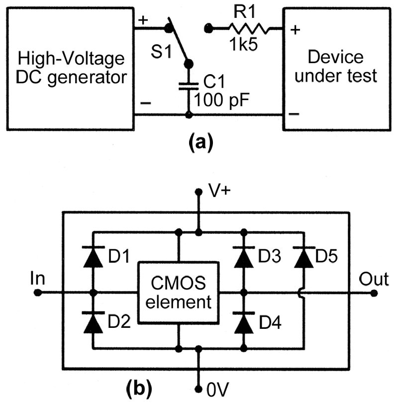
FIGURE 16. (a) Typical electrostatic discharge test circuit, and (b) simple equivalent of a CMOS digital IC element.
Figure 16(b) shows the basic form of a CMOS element’s internal protection circuitry. Here, D1 or D2 conduct if IN tries to go above V+ or below 0V; D3 or D4 conduct if OUT tries to go above V+ or below 0V. D5 conducts if 0V tries to go above V+; D5 also conducts in the zener mode if V+ goes more than about 20V above 0V.
It is important to understand the meaning of these CMOS static discharge protection tests. Suppose that a 3 kV test voltage is applied between the IC’s reverse-connected 0V and V+ pins. Under this condition, D5 is forward biased, and C1 discharges via D5 and R1; R1 limits C1’s peak discharge current to 2A and gives it a basic time constant of 150 nS. Thus, D5 passes only a very brief spike of forward current as C1 discharges. If D1’s thermal time constant is very long compared to the period of the spike, it may not suffer damage from this test, even though it can only handle normal DC currents of (say) 25 mA maximum. Note that the peak voltage appearing across D5 in this test is roughly 1V; most of C1’s 3 kV discharge voltage is lost across R1.
The protection networks used in CMOS ICs are not designed to be effective against massive values of static discharge, such as the several thousand volts that may be generated by a person vigorously prancing about on a nylon carpet, etc. Consequently, when handling naked CMOS ICs, always take sensible precautions against the build-up of large static charges. Do not wear nylon clothing or use nylon mats/carpets in the workshop, and make sure that soldering irons, etc., are correctly grounded.
To be really safe, wear a grounded metal wrist strap when working with CMOS, particularly when soldering. Note, however, that in reality it is very unlikely that you will ever damage a CMOS IC in normal handling, even if you are foolish enough not to wear a grounded wrist strap.
Power Supplies
CMOS ICs of the 4000B and 74HC and 74AC types are designed to operate over a wide range of supply voltages, and can thus be powered from batteries or from regulated or unregulated power supplies. 74HCT and 74ACT types, however, are designed to operate from supplies in the 4.5V to 5.5V range, and must be powered from low-impedance, well-regulated supplies of the types shown in Figures 1 to 3 of last month’s article.
All CMOS ICs generate fast pulse-switching edges. Consequently, most CMOS circuits should be used with a PCB that is designed to give excellent high-frequency supply decoupling to each IC. In general, the PCB’s supply and ground-rail tracks must be as wide as possible (ideally, the 0V track should take the form of a ground plane), all connections and inter-connections should be as short and direct as possible, the PCB’s supply rails should be liberally sprinkled with 4.7 µF Tantalum electrolytic capacitors (at least one per 10 ICs) to enhance l.f. decoupling, and with 10 nF disk ceramics (at least one per four ICs, fitted as close as possible between an IC’s supply pins) to enhance h.f. decoupling.
When experimenting with CMOS ICs, never allow the power supply to be connected in the wrong polarity, since this will cause heavy supply currents to flow through the IC’s protective diode networks (specifically, through D5 in Figure 16) and cause instant damage to the IC’s substrate.
Input Signals
When using CMOS, all IC input signals must — unless the IC is fitted with a Schmitt-type input — have very sharp rising and falling edges. If rise or fall times are too long, they may allow the input terminal to hover in the CMOS element’s linear zone long enough for the element to burst into wild oscillations and generate spasmodic output signals that may disrupt associated circuitry (such as counters and registers, etc). If necessary, slow input signals can be converted into fast ones by feeding them to the IC’s input terminal via CMOS Schmitt elements.
One possible way of damaging CMOS is via a very low impedance input or output signal that is either connected to the CMOS when its power supply is switched off, or is of such large amplitude that it forces the input terminal well above the positive supply line or below the zero-volts rail, thus causing a damaging current to flow through one or more of the IC’s protection diodes (specifically, through Figure 16’s input diodes D1 or D2, or output diodes D3 or D4). The possibility of such damage can be eliminated by wiring a 1K resistor in series with each input/output terminal to limit such currents to safe values of a few milliamps.
Unused Inputs
Unused CMOS input terminals must never be allowed to simply float, but must always be tied to definite logic levels by either connecting them directly to the supply or ground rails (depending on the IC’s logic requirements), or to some other point with well defined logic levels. Figure 17 shows some of the available options.
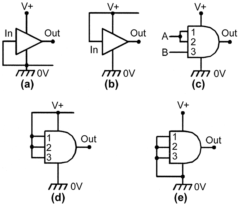
FIGURE 17. Alternative ways of connecting unwanted CMOS inputs (see text).
If the unwanted input is on a multi-input gate, it can be disabled by shorting it to one of the gate’s used inputs, as in Figure 17(c), where a three-input AND gate is shown used as a two-input type. If the IC is a multiple gate type in which an entire gate is unwanted, the gate should be disabled by tying all of its inputs to a common high or low point, as in (d) and (e).
All used CMOS input terminals must also be tied to definite logic levels, and must never be allowed to float. Figure 18 shows three commonly used options.
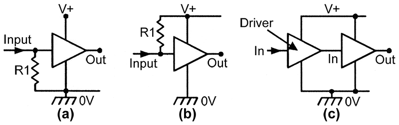
FIGURE 18. All used CMOS inputs must be tied to definite logic levels (see text).
In (a), the input is normally tied low by R1, and in (b) it is normally tied high by R1. In (c), the input is direct-coupled to the output of a driving stage, which determines the input logic level.
Interfacing
An interface circuit is one that enables one type of system to be sensibly connected to a different type of system. In a purely CMOS system, in which all ICs are designed to connect directly together, interface circuitry is usually needed only at the system’s initial input and final output points, to enable them to merge with the outside world via items such as switches, sensors, relays, and indicators, etc.
Occasionally, however, CMOS ICs may be used in conjunction with other logic families (such as TTL), in which case an interface may be needed between the different families. Thus, as far as CMOS is concerned, there are three basic classes of interface circuit, which are: Input interfacing, Output interfacing, and Logic family interfacing.
Input Interfacing
The digital signals arriving at the inputs of a CMOS system must be clean ones with well-defined logic levels and with fast rise and fall times. It is the input interfacing circuitry’s task to convert external input signals into this format. Figures 19 to 22 show four simple examples of such circuitry; these circuits are similar to the TTL designs shown in last month’s Figures 6 to 9, but must use CMOS Schmitt elements and can use any positive supply rail voltage within the operating limits of the CMOS element.
The Figure 19 circuit is designed to clean up the dirty switching signals of push-button switch SW1 and convert them into a form suitable for driving a normal CMOS input. Here, the input of the Schmitt buffer is tied to ground via R1 and R2 and is normally low. When SW1 is closed, C1 rapidly charges up and drives the Schmitt output high, but when SW1 opens again, C1 discharges relatively slowly via R1, and the Schmitt output does not return low again until roughly 20 mS later. The circuit thus ignores the transient switching effects of SW1 noise and contact bounce, etc., and generates a clean output switching waveform with a period that is roughly 20 mS longer than the mean duration of the SW1 switch closure.
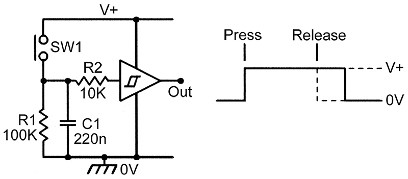
FIGURE 19. CMOS noiseless push-button switch.
Figure 20 shows a circuit that can be used to interface almost any clean digital signal to a normal CMOS input. Here, when the input signal is below 500 mV (Q1’s minimum turn-on voltage), Q1 is cut off and the inverting Schmitt’s output is at logic-0. When the input is significantly above 600 mV, Q1 is driven on and the Schmitt output goes to logic-1. Note that the digital input signal can have any maximum voltage value, and R1 is chosen to simply limit Q1’s base current to a safe value.
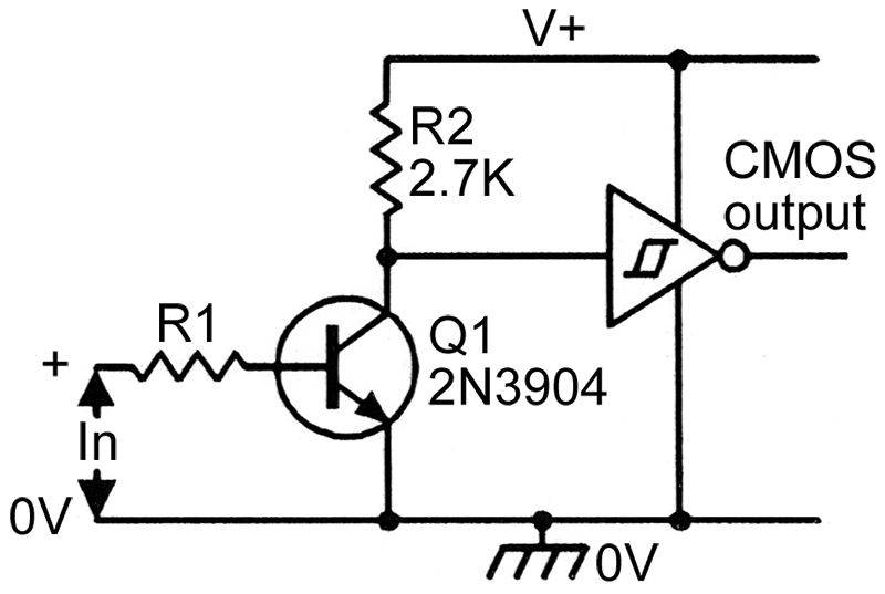
FIGURE 20. CMOS transistor input interface.
Figure 21 is a simple variation of the above circuit, with the transistor built into an optocoupler; the circuit action is such that the Schmitt’s output is at logic-0 when the optocoupler input is zero, and at logic-1 when the input is high; note that the optocoupler provides total electrical isolation between the input and CMOS signals.
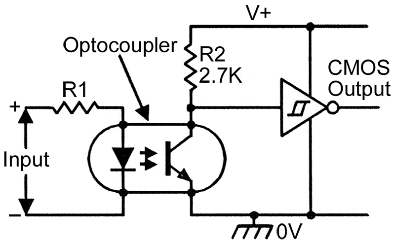
FIGURE 21. CMOS optocoupler input interface.
Finally, Figure 22 is another simple circuit variation, with the basic digital input signal fed to Q1’s base via the R1-C1-R2-C2 low-pass filter network, which eliminates unwanted high-frequency components and thus can convert very dirty input signals (such as those from vehicle contact-breakers, etc.) into a clean CMOS format.
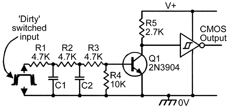
FIGURE 22. CMOS dirty-switching input interface.
Output Interfacing
CMOS totem-pole output stages are designed to source or sink fairly high peak values of output current. Consequently, if the output is shorted directly to the IC’s zero-volts or positive supply rail, the resulting DC output currents can, in some cases, be so high that the IC may be damaged. Thus, when a CMOS IC is used to drive a DC load, its load current must always be limited to a safe value.
Figure 23 shows the typical short circuit output currents of two different manufacturer’s 4000B-series CMOS output stages over the 5V to 15V operating voltage range. In practice, the maximum DC values of these output loads must be limited to 10 mA of current or 100 mW of power dissipation, whichever is the lower of these values.
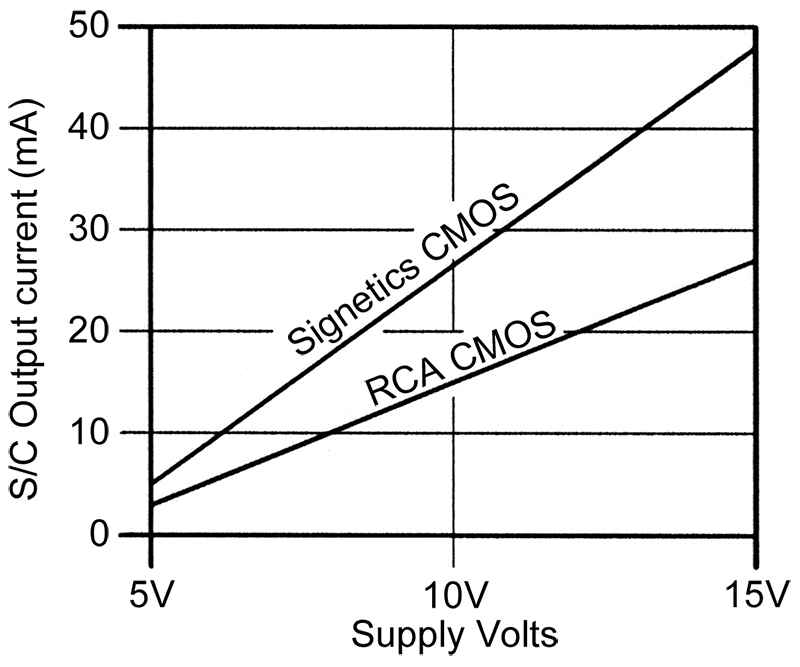
FIGURE 23. Typical 4000B-series short-circuit output currents (at 25 OC).
Figure 24 shows the typical short-circuit output currents of standard and bus driver versions of 74HC-series CMOS output stages over the 2V to 6V operating voltage range. In practice, the maximum DC values of these currents must be limited to 25 mA in standard HC types, and 35 mA in bus driver HC types.
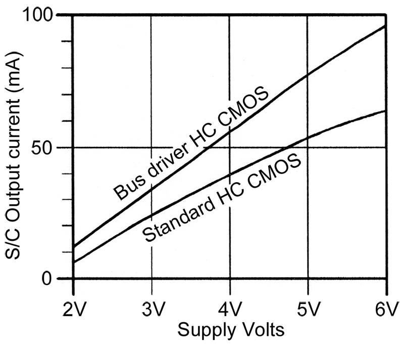
FIGURE 24. Typical 74HC series short-circuit output currents (at 25 OC).
The only time this current limiting matter is likely to present any real problem is when using CMOS to drive some type of LED load (including those at the inputs of optocouplers, etc.). Figures 25 and 26 show basic ways of driving an LED via non-inverting or inverting CMOS elements.
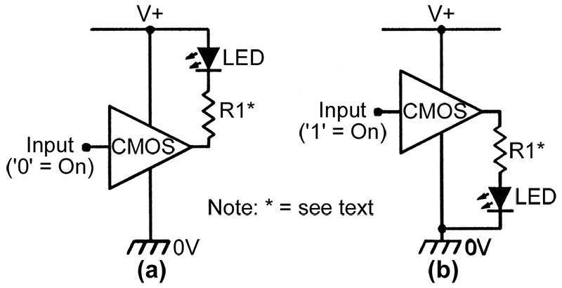
FIGURE 25. LED-driving output interface, using non-inverting CMOS elements.
FIGURE 26. LED-driving output interface, using inverting CMOS elements.
Note in these circuits that R1 sets the LED’s ON current, and has a value of [(V+ - Vs)/I] - Rx, where V+ is the supply voltage, Vs is the LED’s saturation voltage (typically 2.0 to 2.5 volts), I is the LED’s ON current (in amps), and Rx is the CMOS elements saturation resistance (and varies widely with voltage, current, and with individual ICs).
Typically, however, Vs equals 2.2V, and Rx has an approximate value of 100Ω in a standard 74HC output or 70Ω in a bus driver output, or 500Ω in a standard 4000B output. Thus, to set the LED current at 10 mA, R1 needs a value of about 180Ω in a 5V standard 74HC circuit, 220Ω in a 5V bus driver 74HC circuit, 270Ω in a 10V 4000B circuit, or 820Ω in a 15V 4000B circuit.
Note that CMOS outputs can be used to drive any of the basic TTL output interface circuits shown in Figures 12 to 17 in the last installment (Part 3) of this series by simply wiring a current-limiting resistor in series with the CMOS output, to limit its output current to a safe value.
Logic Family Interfacing
It is generally bad practice to mix different logic families in any system, but on those occasions where it does occur, the mix is usually made between TTL and CMOS devices. Figures 18 to 23 of last month’s article showed six basic ways of interfacing TTL and CMOS ICs. Note that 74HCT and 74ACT types of CMOS ICs are designed to be directly driven from TTL outputs, without need for special interfacing methods. Also note that standard 4000B-series and 74CXX-series CMOS elements have very low fan-outs and can only drive a single standard TTL or LS TTL element, but 74HCXX-series (and 74ACXX-series) CMOS elements have excellent fan-outs and can directly drive up to two standard TTL inputs, or 10 LS TTL inputs, or 20 ALS TTL inputs.
Most TTL ICs with open-collector (OC) outputs have output-voltage ratings of at least 15V (but the main IC has a normal 5V rating), and can be interfaced to the input of a CMOS logic IC by using the connections shown in Figure 27.
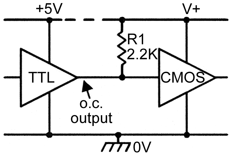
FIGURE 27. TTL (open collector output) to CMOS interface, using common or independent +ve rails.
Here, R1 acts like a pull-up resistor, and the CMOS IC can either share the 5V supply of the TTL IC, or can use its own 5V to 15V positive supply rail. Similarly, a CMOS IC with an open-drain (OD) output can be interfaced to a normal TTL input by using the connections shown in Figure 28 but, in this case, the two ICs must share a common 5V supply rail.
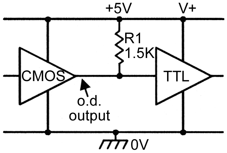
FIGURE 28. CMOS (open drain output) to TTL interface.
CMOS Supply Pin Notations
Most digital ICs have only two supply pins, one of which connects to a circuit’s positive supply rail, and the other to the zero volts rail. In TTL ICs, these pins are conventionally notated VCC and GND respectively, with the VCC notation implying that the positive rail usually connects to the collector sides of the IC’s internal transistors.
When 4000-series CMOS ICs were first introduced, the supply pins were renamed VDD and VSS respectively, implying that the positive rail usually connects to the drain side of the IC’s internal IGFETs, and the zero-volts rail to the source sides. These notations are, in fact, quite ambiguous, but are still widely used in CMOS manufacturer’s data books.
When CMOS was first used as a C sub-family in the 74-series range of ICs, its supply pins were renamed VCC and GND, to comply with normal TTL conventions, and this system has subsequently been used on all other CMOS sub-families used in the 74-series of ICs. In recent times this same system has started to be used on the 4000-series of CMOS ICs, as well, and the current situation is that a CMOS IC positive supply terminal may be notated VCC or VDD, depending on the whim of the individual manufacturer. NV