SEVEN-SEGMENT DISPLAYS
A very common requirement in modern electronics is that of displaying alphanumeric characters. Digital watches, pocket calculators, and digital multimeters and frequency meters are all examples of devices that use such displays. The best known type of alphanumeric indicator is the seven-segment display, which comprises seven independently-accessible photoelectric segments (such as LEDs or LCDs, or gas-discharge or fluorescent elements, etc.) arranged in the form shown in Figure 1.
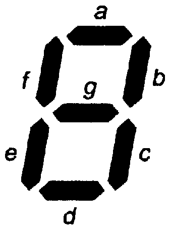
FIGURE 1. Standard form and notations of a seven-segment display.
The segments are conventionally notated from a to g in the manner shown in the diagram, and it is possible to make them display any number (numeral) from 0 to 9 or alphabetic character from A to F (in a mixture of upper and lower case letters) by activating these segments in various combinations, as shown in the truth table in Figure 2.
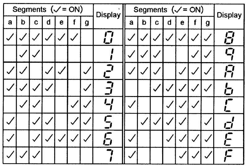
FIGURE 2. Truth table for a seven-segment display.
Practical seven-segment display devices must be provided with at least eight external connection terminals; seven of these give access to the individual photoelectric segments, and the eighth provides a common connection to all segments. If the display is an LED type, the seven individual LEDs may be arranged in the form shown in Figure 3, in which all LED anodes are connected to the common terminal, or they may be arranged as in Figure 4, in which all LED cathodes are connected to the common terminal. In the former case, the device is known as a common-anode seven-segment display; in the latter case, the device is known as a common-cathode seven-segment display.
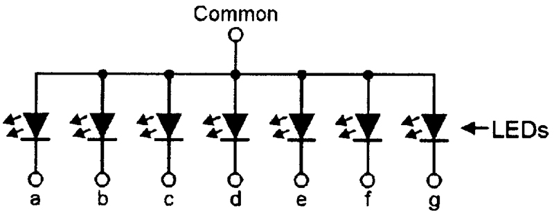
FIGURE 3. Schematic diagram of a common-anode seven-segment LED display.
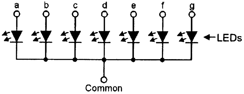
FIGURE 4. Schematic diagram of a common-cathode seven-segment LED display.
SEVEN-SEGMENT DISPLAY/DRIVERS
In most practical applications, seven-segment displays are used to give a visual indication of the output states of digital ICs such as decade counters and latches, etc. These outputs are usually in four-bit BCD (Binary Coded Decimal) form and are not suitable for directly driving seven-segment displays. Consequently, special BCD-to-seven-segment decoder/driver ICs are available to convert the BCD signal into a form suitable for driving these displays, and are connected between the BCD signals and the display in the manner shown in Figure 5.
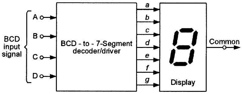
FIGURE 5. Basic connections of a BCD-to-seven-segment decoder/driver IC.
The table in Figure 6 shows the relationship between the BCD signals and the displayed seven-segment numerals.
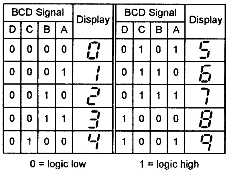
FIGURE 6. Truth table of a BCD-to-seven-segment decoder/driver.
In practice, BCD-to-seven-segment decoder/driver ICs are usually available in a dedicated form that is suitable for driving only a single class of display unit, e.g., either common-anode LED type, or common-cathode LED type, or liquid crystal displays (LCDs). Figures 7 to 9 show the methods of interconnecting each of these IC and display types.
Note in the case of the LED circuits (Figures 7 and 8) that, if the IC outputs are unprotected (as in the case of most TTL ICs), a current-limiting resistor must be wired in series with each display segment (about 150R with a 5V supply, or 680R at 15V); most CMOS ICs have internally current-limited outputs, and do not require the use of these external resistors. To drive a common-anode display (Figure 7), the driver must have an active-low output, in which each segment-driving output is normally high, but goes low to turn a segment on. To drive a common-cathode display (Figure 8), the driver must have an active-high output.
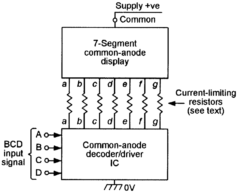
FIGURE 7. Method of driving a common-anode LED display.
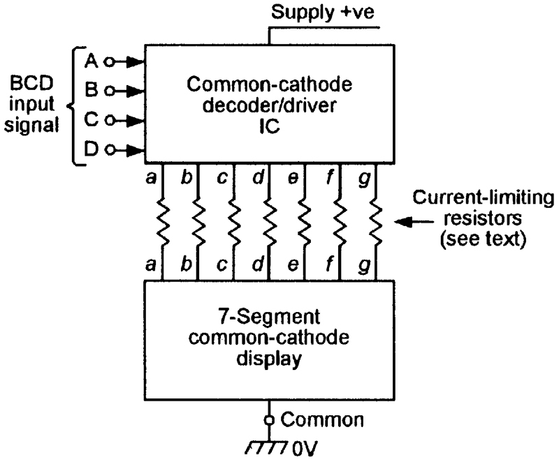
FIGURE 8. Method of driving a common-cathode LED display.
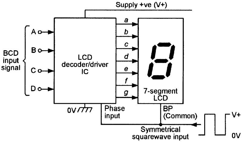
FIGURE 9. Method of driving a liquid-crystal display (LCD).
In the Figure 9 LCD-driving circuit, the display’s common BP (back-plane) terminal and the IC’s phase input terminals must be driven by a symmetrical squarewave (typically 30Hz to 200Hz) that switches fully between the two supply rail voltages (0V and V+), as shown. The full explanation for this is a little complicated, as follows.
To drive an LCD segment, the driving voltage must be applied between the segment and BP terminals. When the voltage is zero, the segment is effectively invisible. When the drive voltage has a significant positive or negative value, however, the segment becomes effectively visible, but if the drive voltage is sustained for more than a few hundred milliseconds, the segment may become permanently visible and be of no further value.
The way around this problem is — in principle — to drive the segment on via a perfectly symmetrical squarewave that switches alternately between identical positive and negative voltages, and thus has zero DC components and will not damage the LCD segment even if sustained permanently. In practice, this type of waveform is actually generated with the aid of an EX-OR True/Complement generator, connected as shown in Figure 10(a).
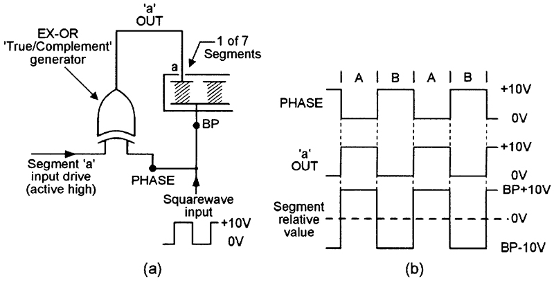
FIGURE 10. Basic LCD segment-drive circuit (a), and voltage-doubling ‘bridge-driven’ segment waveforms (b).
In Figure 10(a), the basic segment ‘a’ input drive (which is active-high) is connected to one input of the EX-OR element, and the other EX-OR input terminal (which is notated PHASE) is driven by a symmetrical squarewave that switches fully between the circuit’s supply rail voltages (shown as 0V and +10V) and is also applied to the LCD display’s BP pin.
When the segment ‘a’ input drive is low, the EX-OR element gives a non-inverted (in-phase) ‘a’ output when the squarewave is at logic-0, and an inverted (anti-phase) ‘a’ output when the squarewave is at logic-1, and thus produces zero voltage difference between the ‘a’ segment and BP points under both these conditions. The segment is thus turned off under these conditions.
When the segment ‘a’ input drive is high, the EX-OR element gives the same phase action as just described, but in this case, the ‘a’ OUT pin is high and BP is low when the squarewave is at logic-0, and ‘a’ OUT is low and BP is high when the squarewave is at logic-1. The segment is thus turned on under these conditions.
Figure 10(b) shows the circuit waveforms that occur when the ‘a’ segment is turned on, with the ‘a’ segment and BP driven by anti-phase squarewaves. Thus, in part A of the waveform, the segment is 10V positive to BP, and in part B, it is 10V negative to BP, so the LCD is effectively driven by a squarewave with a peak-to-peak value of 20V, but with zero DC value. This form of drive is generally known as a voltage-doubling ‘bridge drive’ system. In practice, many LCD-driving ICs (such as the 4543B) incorporate this type of drive system in the form of a seven-section EX-OR gate array interposed in series with the segment output pins, with access to its common line via a single PHASE terminal.
Note that any active-high seven-segment LED-driving decoder IC can be used to drive a seven-segment LCD display by interposing a bridge-driven seven-section EX-OR array between its segment output pins and the segment pins of the LCD display, as shown in Figure 11, in which a 74LS48 TTL IC is used in this specific way.

FIGURE 11. Basic way of using an active-high LED-driving decoder IC (such as the 74LS48 TTL type) to drive a seven-segment LCD via a bridge-driven seven-section EX-OR array.
CASCADED DISPLAYS
In most practical seven-segment display applications, several sets of displays and matching decoder/driver ICs are cascaded and used to make multi-digit display systems. Figure 12, for example, shows a very simple way of using three sets of decoder/driver ICs and displays in conjunction with three decade counter ICs to make a simple digital-readout frequency meter. Here, the amplified external frequency signal is fed to the input of the series-connected counters via one input of a two-input AND gate, which has its other (GATE) input waveform derived from a built-in timebase generator.
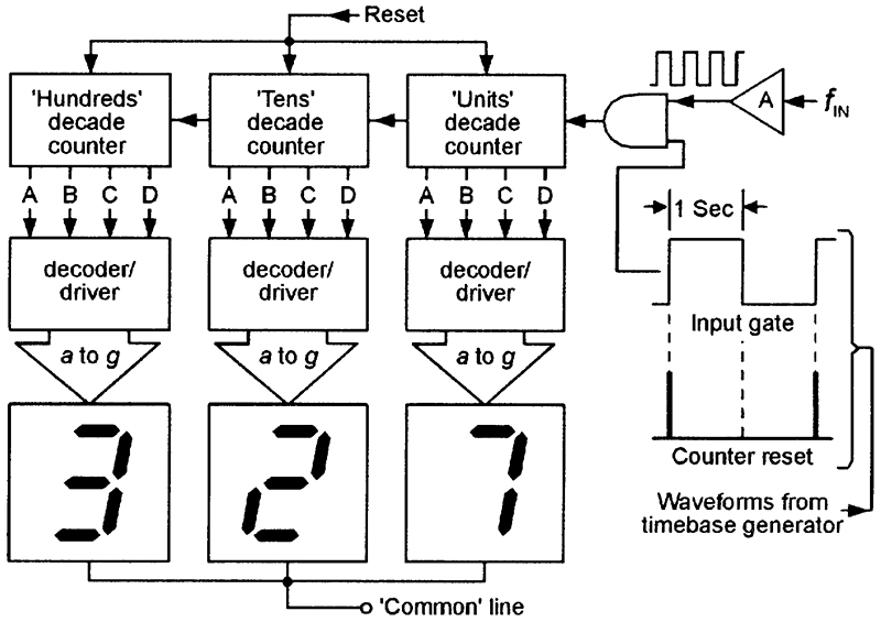
FIGURE 12. Simple digital frequency meter circuit.
The circuit’s operating sequence is as follows:
When the timebase GATE input signal is low, the AND gate is closed and no input signals reach the counters. At the moment that the timebase GATE signal switches high, a brief RESET pulse is fed to all three counters, setting them all to zero count; simultaneously, the input gate opens, and remains open for a period of precisely one second, during which time the input-frequency pulses are summed by the counters.
At the end of the one second period, the gate closes and the timebase GATE signal goes low again, thus ending the count and enabling the displays to give a steady reading of that second’s total pulse count (and thus the mean signal frequency). The whole process then repeats again one second later, when the timebase GATE signal again goes high.
DISPLAY LATCHING
The simple cascaded system described previously suffers from a major defect, in that the display becomes a blur during the actual counting period, becoming stable and readable only when each count is completed and the input gate is closed. This ‘blur-and-read’ type of display is very annoying to watch.
Figure 13 shows an improved frequency meter circuit that uses display latching to overcome the above defect. Here, a four-bit data latch is wired between the output of each counter and the input of its decoder/driver IC.
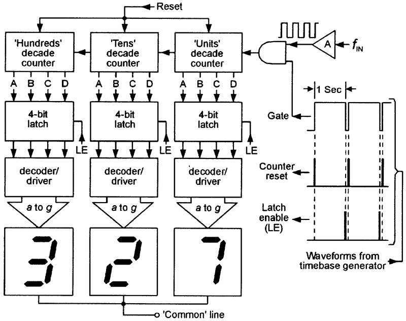
FIGURE 13. Improved digital frequency meter circuit.
This circuit operates as follows:
At the moment that the timebase GATE signal goes high, a RESET pulse is fed to all counters, setting them to zero. Simultaneously, the input gate is opened and the counters start to sum the input signal pulses. This count continues for precisely one second, and during this period, the four-bit latches prevent the counter output signals from reaching the display drivers; the display thus remains stable during this period.
At the end of the one second count period, the AND gate closes and terminates the count, and simultaneously a brief LATCH ENABLE pulse is fed to all latches, causing the prevailing BCD outputs of each counter to be latched into memory and then fed to the display via the decoder/driver ICs, thus causing the display to give a steady reading of the total pulse count (and thus the input frequency).
A few moments later, the sequence repeats again, with the counters resetting and then counting the input frequency pulses for one second, during which time the display gives a steady reading of the results of the previous count, and so on.
The Figure 13 circuit thus generates a stable display that is updated once every second; in practice, the actual count period of this and the Figure 12 circuit can be made any decade multiple or submultiple of one second, provided that the output display is suitably scaled.
Note that a three-digit frequency meter can indicate maximum frequencies of 999Hz when using a one-second timebase, 9.99kHz when using a 100mS timebase, 99.9kHz when using a 10mS timebase, and 999kHz when using a 1mS timebase. In reality, many decoder/driver ICs have built-in four-bit data latches.
MULTIPLEXING
Note from the Figure 12 and 13 circuits that a total of at least 21 connections must be made between the IC circuitry and the seven-segment displays of a three-digit read-out unit; a total of at least 70 connections are needed if a 10-digit display is used. In reality, the number of IC-to-display connections can be greatly reduced by using the technique known as multiplexing. This technique can be understood with the aid of Figures 14 and 15.
Figure 14 shows how each digit of a three-digit common-cathode LED display can be individually activated using a total of only 10 external connections; the circuitry to the left of the dotted line should be regarded as ‘electronic,’ and to the right of the line as ‘display’ circuitry.
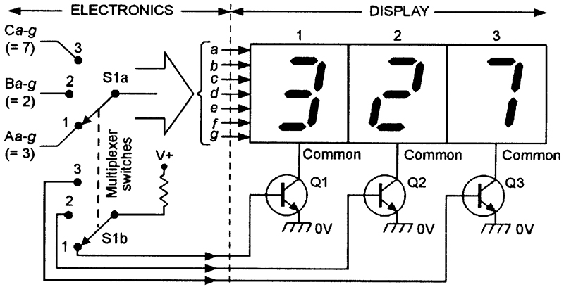
FIGURE 14. Method of multiplexing a three-digit common-cathode LED display.
In the display, all a segments are connected together, as also are all other (b to g) sets of segments, so that a total of only seven external a-to-g, connections are made to the display irrespective of the number of digits used.
Note, however, that none of the seven-segment displays are influenced by signals on these segment wires unless a display is enabled by connecting its common terminal to ground, and in Figure 14, this is achieved by activating switching transistors Q1 to Q3 via suitable external signals, which require the use of only one additional connection per display digit.
Note in Figure 14 that three different sets of segment data can be selected via switch S1a which, in reality, would take the form of a ganged seven-pole three-way electronic switch (with one pole dedicated to each of the seven segment lines), and that any one of the three display digits can be selected via S1b and Q1 to Q3. These switches are ganged together and provide the actual multiplexer action, and should be regarded as fast-acting electronic switches that repeatedly switch through positions 1, 2, and 3. The operating sequence of the circuit is as follows.
Assume initially that the switch is in position 1. Under this condition, S1a selects segment data Aa-g, and S1b activates display 1 via Q1, so that display 1 shows the number 3. A few moments later, the switch jumps to position 2, selecting segment data Ba-g and activating display 2 via Q2, so that display 2 shows the number 2.
A few moments later, the switch jumps to position 3, causing display 3 to show the number 7. A few moments later, the whole cycle starts to repeat again, and so on add infinitum.
In practice, about 50 of these cycles occur each second, so the eye does not see the displays being turned on and off individually, but sees them as an apparently steady display that shows the number 327, or whatever other number is dictated by the segment data.
Note from the above description that, since each display is turned on for only one-third of each cycle, the mean current consumption of each display is one-third of the peak display current, and the LED brightness levels are correspondingly reduced. In practical multiplexers, the peak display current is made fairly high, to give adequate display brightness.
Figure 15 shows an example of an improved multiplexing (MUX) technique, as applied to a three-digit frequency meter. In this case, the MUX is interposed between the outputs of the three BCD data latches and the input of the BCD-to-seven- segment decoder/driver IC. This technique has two major advantages.
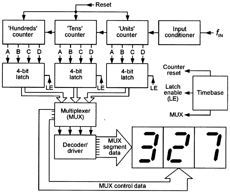
FIGURE 15. Realistic implementation of the multiplexing technique in a three-digit frequency meter.
First, it calls for the use of only a single decoder/driver IC, irrespective of the number of readout digits used. Second, it calls for the use of a MUX incorporating only five ganged three-way sequencing switches (one for the control data and four for the BCD data), rather than the eight ganged three-way switches (one for the control data and seven for the segment data) called for in the Figure 14 system.
In practice, all of the counting, latching, multiplexing, decoding, timing, and display-driving circuitry of Figure 15 (and a great deal more) can easily be incorporated in a single LSI (large scale integration) chip that needs only 20 or so pins to make all necessary connections to the power supply, displays, and inputs, etc. Thus, a complete four-digit counter can be implemented using a dedicated IC in a circuit such as that shown in Figure 16, or a 3 1/2-digit DVM (digital voltmeter) can be implemented using a circuit such as that shown in Figure 17.

FIGURE 16. A four-digit counter circuit, using a LSI chip.
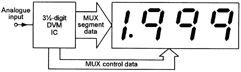
FIGURE 17. A 3 1/2-digit DVM using a LSI chip.
RIPPLE BLANKING
If the basic four-digit Figure 16 circuit is used to measure a count of 27, it will actually give a reading of 0027, unless steps are taken to provide automatic suppression of the two (unwanted) leading zeros. Similarly, if the 3 1/2-digit circuit of Figure 17 is used to measure 0.1 volts, it will actually give a display of 0.100 volts, unless steps are taken to provide automatic suppression of the two (unwanted) trailing zeros.
In practice, automatic blanking of leading and/or trailing zeros can be obtained by using a ripple blanking technique, as illustrated in Figures 18 and 19. In these diagrams, each decoder/driver IC has a BCD input and a seven-segment output, and is provided with ripple blanking input (RBI) and output (RBO) terminals. If these terminals are active high, they will have the following characteristics.
If the RBI terminal is held low (at logic-0), the seven-segment outputs of the IC are enabled but the RBO terminal is disabled (held low). If the RBI terminal is biased high (at logic-1), the seven-segment outputs become disabled in the presence of a BCD ‘0000’ input (= decimal zero), and the RBO output goes high under the same condition.
Thus, the RBO terminal is normally low and goes high only if a BCD ‘0000’ input is present at the same time as the RBI terminal is high. With these characteristics in mind, refer now to Figures 18 and 19.
Figure 18 shows the ripple blanking technique used to provide leading-zero suppression in a four-digit display that is reading a count of 207. Here, the RBI input of the thousands or most significant digit (MSD) decoder/driver is tied high, so this display is automatically blanked in the presence of a zero, under which condition the RBO terminal is high.
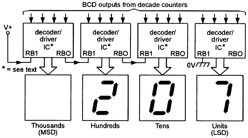
FIGURE 18. Ripple-blanking used to give leading-zero suppression in a four-digit counter.
Consequently, the RBI terminal of the hundreds IC is high, so its display reads 2, and the RBO terminal is low. The RBI input of the tens unit is thus also low, so its display reads 0 and its RBO output is low. The least significant digit (LSD) is that of the units readout, and this does not require zero suppression; consequently, its RBI input is grounded and it reads 7. The display thus gives a total reading of 207.
Note in the Figure 18 leading zero suppression circuit that ripple blanking feedback is applied backwards, from the MSD to the LSD. Figure 19 shows how trailing zero suppression can be obtained by reversing the direction of feedback, from the LSD to the MSD. Thus, when an input of 1.1 volts is fed to this circuit, the LSD is blanked, since its BCD input is ‘0000’ and its RBI input is high. Its RBO terminal is high under this condition, so the 100ths digit is also blanked in the presence of a ‘0000’ BCD input.
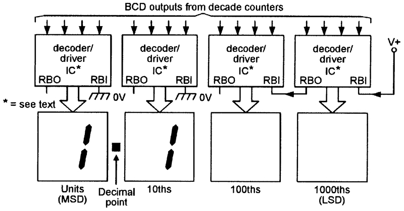
FIGURE 19. Ripple-blanking used to give trailing-zero suppression of the last two digits of a 3 1/2-digit DVM readout.
Practical decoder/driver ICs are often (but not always) provided with ripple blanking input and output terminals; often, these are active low. If a decoder/driver IC does not incorporate integral ripple blanking logic, it can usually be obtained by adding external logic similar to that shown in Figure 20, with the RBO terminal connected to the BLANKING input pin of the decoder/driver IC.
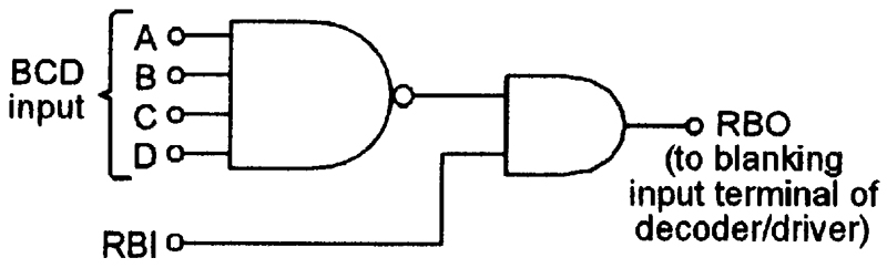
FIGURE 20. DIY ripple-blanking logic (active-high type).
In Figure 20 (an active high circuit), the output of the four-input NOR gate goes high only in the presence of a ‘0000’ BCD input, and the RBO output goes high only if the decimal zero input is present while RBI is high.
The next and last episode of this two-part feature will describe practical seven-segment decoder/driver ICs and circuits. NV