The opening episode of this special feature explained the basic operating and usage principles of seven-segment alphanumeric displays.
This concluding episode deals with practical seven-segment decoder/driver ICs.
PRACTICAL DECODER/DRIVER ICs
Decoder/driver ICs are available in both TTL and CMOS forms. Some of these devices have integral ripple-blanking facilities, others have built-in data latches, and a few even have built-in decade counter stages, etc. The rest of this article describes a few of the most popular of these devices.
The 74LS47 and 74LS48
These seven-segment decoder/driver ICs are members of the LS TTL family. They have integral ripple-blanking facilities, but do not incorporate data latches. Figure 1 shows the functional diagrams and pin designations of these devices, each of which is housed in a 16-pin DIL package.
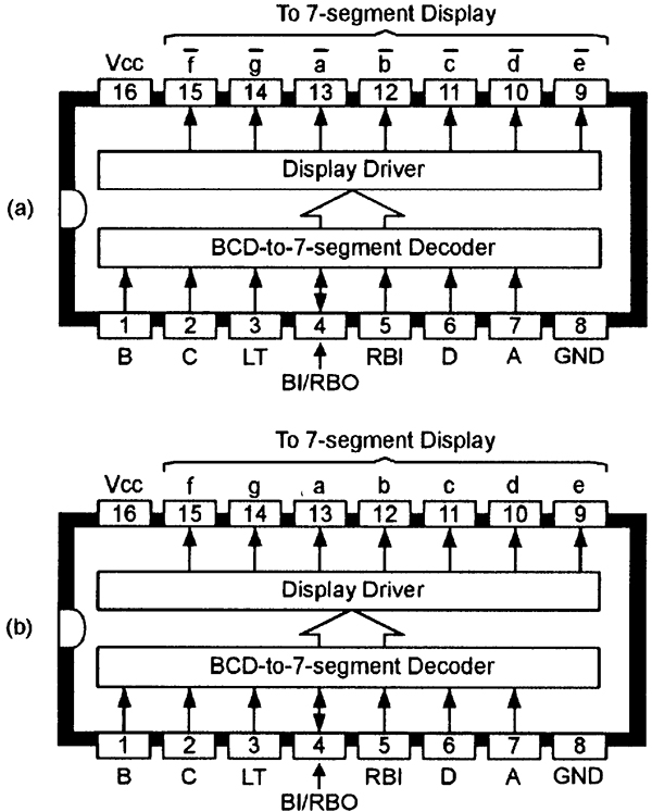
FIGURE 1. Functional diagram of the (a) 74LS47 and (b) 74LS48 BCD-to-seven-segment decoder/driver ICs.
The 74LS47 has active-low outputs designed for driving a common-anode LED display via external current-limiting resistors (Rx), as shown in Figure 2.
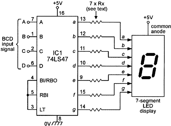
FIGURE 2. Basic way of using a 74LS47 IC to drive a common-anode LED display.
The 74LS48 has active-high outputs designed for driving a common-cathode LED display in a manner similar to that of Figure 2, but with the display’s common terminal taken to ground. The Rx resistors must limit the segment currents to less than 24mA in the 74LS47, and less than 6mA in the 74LS48. The 74LS48 can be used to drive a seven-segment LCD display by using the connections already shown in last month’s Figure 11.
Note from Figure 1 that each of these ICs has three input ‘control’ terminals, these being designated LT (Lamp Test), BI/RBO, and RBI. The LT terminal drives all display outputs on when the terminal is driven to logic 0 with the RBO terminal open or at logic 1.
When the BI/RBO terminal is pulled low, all outputs are blanked; this pin also functions as a ripple-blanking output terminal. Figure 3 shows how to connect the ripple-blanking terminals to give leading zero suppression on the first three digits of a four-digit display.
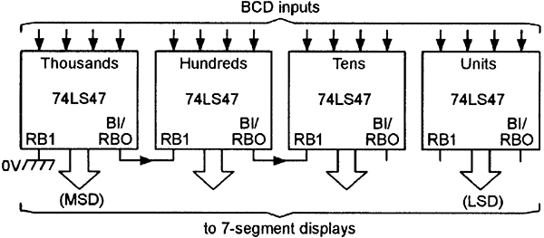
FIGURE 3. Method of applying leading-zero suppression to the first three digits of a four-digit display using 74LS47 ICs.
The 4511B
The most popular CMOS 4000B-series BCD-to-seven-segment LED-driving IC is the 4511B (also available as the 74HC4511), which has an integral four-bit data latch, but has no built-in ripple-blanking facilities.
Figure 4 shows the functional diagram and pin notations of the device, which can use any power source in the 5V to 15V range. The IC is ideally suited to driving common cathode LED displays, and uses NPN bipolar output transistor stages that can each source up to 25mA.
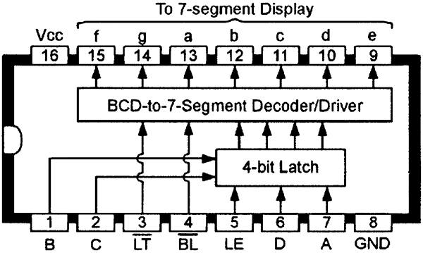
FIGURE 4. Functional diagram and pin notations of the 4511B seven-segment latch/decoder/LED-driver IC.
The 4511B is very easy to use, and has only three input control terminals; of these, the not-LT (pin 3) pin is normally tied high, but turns on all seven segments of the display when pulled low.
The not-BL (pin 4) terminal is also normally tied high, but blanks (turns off) all seven segments when pulled low.
Finally, the LE (latch enable) terminal (pin 5) enables the IC to give either direct or latched decoding operation. When LE is low, the IC gives direct decoding operation, but when LE is taken high, it freezes the display.
The 4511B can be used to drive most popular types of seven-segment displays. Figure 5 shows the basic connections for driving a common-cathode LED display.

FIGURE 5. Basic way of using the 4511B to drive a seven-segment common-cathode LED display.
A current-limiting resistor (Rx) must be wired in series with each display segment and must have its value chosen to limit the segment current below 25mA.
Figures 6, 7, and 8 show how to modify the above circuit to drive LED common-anode displays, gas discharge displays, and low-brightness fluorescent displays, respectively.
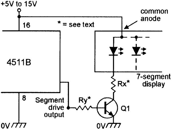
FIGURE 6. Driving a common-anode LED display.
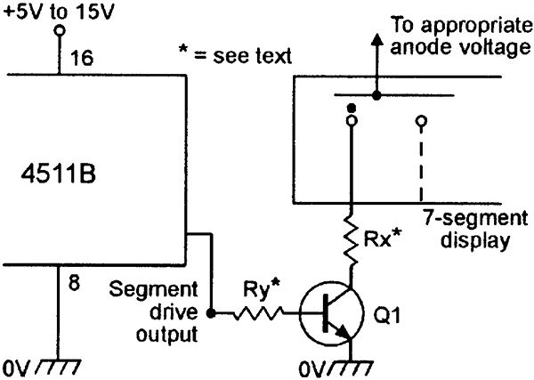
FIGURE 7. Driving a gas discharge readout.
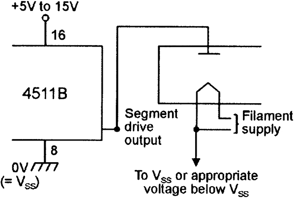
FIGURE 8. Driving a low-brightness fluorescent readout.
Note in the cases of Figures 6 and 7 that an NPN buffer transistor must be interposed between each output drive segment and the input segment of the display.
In each case, Rx determines the operating segment current of the display, and Ry determines the base current of the transistor.
The 4511B can also be used to drive seven-segment liquid-crystal displays by using an external squarewave ‘phase’ signal and a set of EX-OR gates in a configuration similar to that of last month’s Figure 11. In practice, however, it is far better to use a 4543B IC for this particular application.
The 4543B
The most popular 4000B-series BCD-to-seven-segment LCD-driving IC is the 4543B (also available as the 74HC4543), which has a built-in data latch. Figure 9 shows the IC’s functional diagram and pin notations.
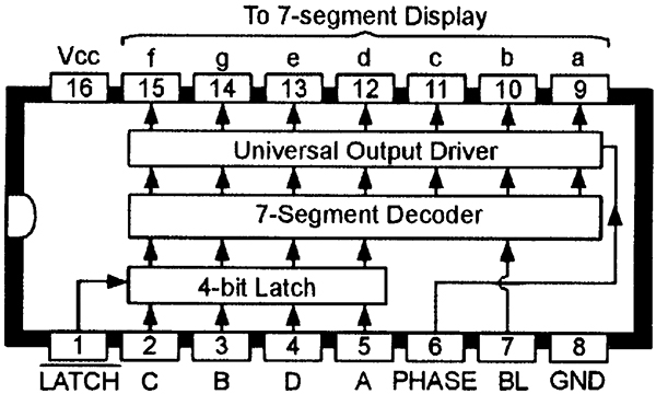
FIGURE 9. Functional diagram and pin notations of the 4543B universal seven-segment latch/decoder/driver IC.
The device incorporates an EX-OR array (of the type shown in last month’s Figure 11) in its output driver network, which can source or sink several milliamps of output current. This feature enables the IC to act as a universal unit that can drive common-cathode or common-anode LED or liquid-crystal seven-segment displays with equal ease, as shown in Figures 10 to 13.
The 4543B has three input control terminals, these being designated not-LATCH, PHASE, and BL (BLANK). In normal use, the not-LATCH terminal is biased high and the BL terminal is tied low. The state of the PHASE terminal depends on the type of display that is being driven. For driving LCD readouts, a squarewave (roughly 50Hz, swinging fully between the GND and Vcc values) must be applied to the PHASE terminal. For driving common-cathode LED displays, PHASE must be grounded. For driving common-anode displays, PHASE must be tied to logic high.
The display can be blanked at any time by driving the BL terminal to the logic-1 level. When the not-LATCH terminal is in its normal high (logic-1) state, BCD inputs are decoded and fed directly to the seven-segment output terminals of the IC. When the not-LATCH terminal is pulled low, the BCD input signals that are present at the moment of transition are latched into memory and fed (in decoded form) to the seven-segment outputs until the not-LATCH pin returns to the high state.
Figure 10 shows basic ways of using the 4543B to drive common-cathode and common-anode seven-segment LED displays; the ‘R’ resistance value must limit the output drive current to below 10mA per segment.
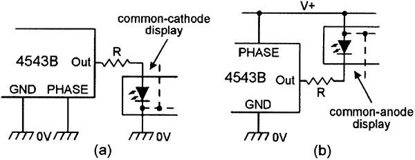
FIGURE 10. Way of using the 4543B to drive (a) common-cathode or (b) common-anode seven-segment LED displays.
Figure 11 shows the basic way of using the 4543B to drive a seven-segment LCD, and Figures 12 and 13 show it used to drive other types of seven-segment displays. In Figure 12, Rx sets the segment current of the display and Ry sets the base current of the transistor (10mA maximum).
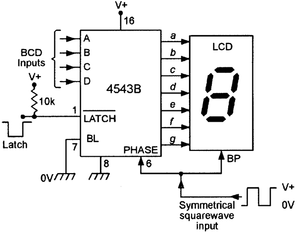
FIGURE 11. Way of using the 4543B to drive a seven-segment LCD.
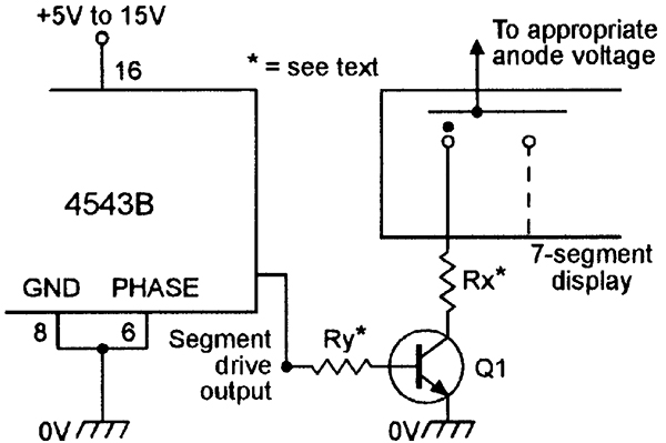
FIGURE 12. Driving a gas discharge readout with a 4543B.
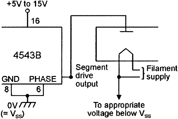
FIGURE 13. Driving a fluorescent readout with a 4543B.
The 4026B
The 4026B IC is a complete decade counter with integral decoder/driver circuitry that can directly drive a seven-segment common-cathode LED display. The segment output currents are internally limited to about 5mA at 10V or 10mA at 15V. Enabling the display can be connected directly to the outputs of the IC without the use of external current-limiting resistors. The IC does not incorporate a data latch and has no facility for ripple blanking. Figure 14 shows the functional diagram and pin notations of the 4026B.
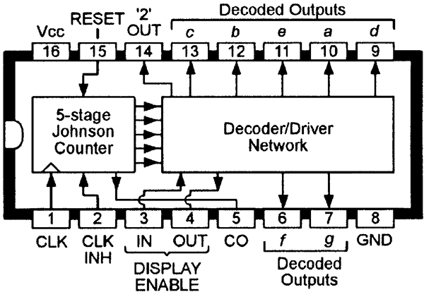
FIGURE 14. Functional diagram and pin notations of the 4026B decade counter with seven-segment display driver.
The 4026B has four input control terminals, and three auxiliary output terminals. The input terminals are designated CLK (CLOCK), CLK INH (CLOCK INHIBIT), RESET, and DISPLAY ENABLE IN. The IC incorporates a Schmitt Trigger on its CLK input line, and clock signals do not have to be pre-shaped. The counter is reset to zero by driving the RESET terminal high.
The CLK INH terminal must be grounded to allow normal counting operation. When CLK INH is high, the counters are inhibited. The display is blanked when the DISPLAY ENABLE IN terminal is grounded. The DISPLAY ENABLE IN terminal must be high for normal operation. Thus, in normal operation, the RESET and CLK INH terminals are grounded and the DISPLAY ENABLE IN terminal is held positive, as shown in Figure 15.
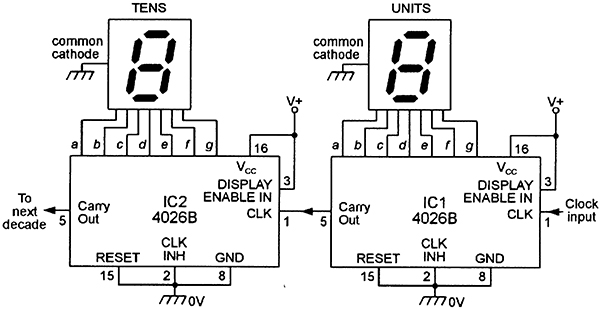
FIGURE 15. Basic method of cascading 4026B ICs.
The three auxiliary output terminals of the 4026B are designated DISPLAY ENABLE OUT, CO (CARRY OUT), and ‘2’ OUT. The DISPLAY ENABLE OUT signal is a slightly delayed copy of the DISPLAY ENABLE IN input signal. The CO signal is a symmetrical square- wave at one-tenth of the CLK input frequency, and is useful in cascading 4026B counters. The ‘2’ OUT terminal goes low only on a count of 2. Figure 15 shows the basic circuit connections to be used when cascading stages.
The 4033B
This device (see Figure 16) can be regarded as a modified version of the 4026B, with the DISPLAY ENABLE IN and DISPLAY ENABLE OUT terminals eliminated and replaced by ripple blanking input (RBI) and output (RBO) terminals, and with the ‘2’ OUT terminal replaced with a LT (LAMP TEST) terminal which activates all output segments when biased high.
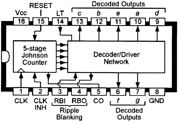
FIGURE 16. Functional diagram and pin notations of the 4033B decade counter with seven-segment display driver.
In normal use, the RESET, CLK INH, and LT terminals are all grounded and the RBI terminal is made positive, as shown in Figure 17. This configuration does not provide blanking of unwanted leading and/or trailing zeros.
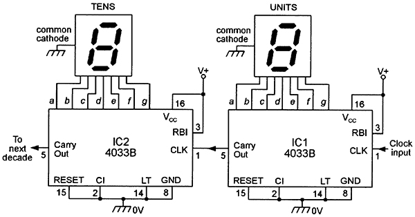
FIGURE 17. Basic method of cascading 4033B ICs (without zero suppression).
If cascaded 4033B ICs are required to give automatic leading-zero suppression, the basic Figure 17 circuit must be modified as shown in Figure 18 to provide ripple-blanking operation. Here, the RBI terminal of the most significant digit (MSD) is grounded, and its RBO terminal is connected to the RBI terminal of the next least-significant stage.
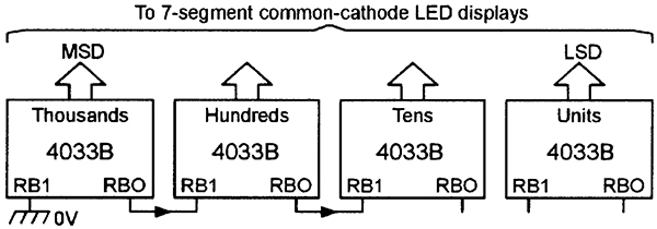
FIGURE 18. Method of modifying the Figure 17 circuit to give automatic leading-zero suppression.
This procedure is repeated on all except the LSD, which does not require zero suppression. If trailing-zero suppression is required, the direction of ripple-blanking feedback must be reversed with the RBI terminal of the LSD grounded and its RBO terminal wired to the RBI terminal of the next least-significant stage, and so on. NV