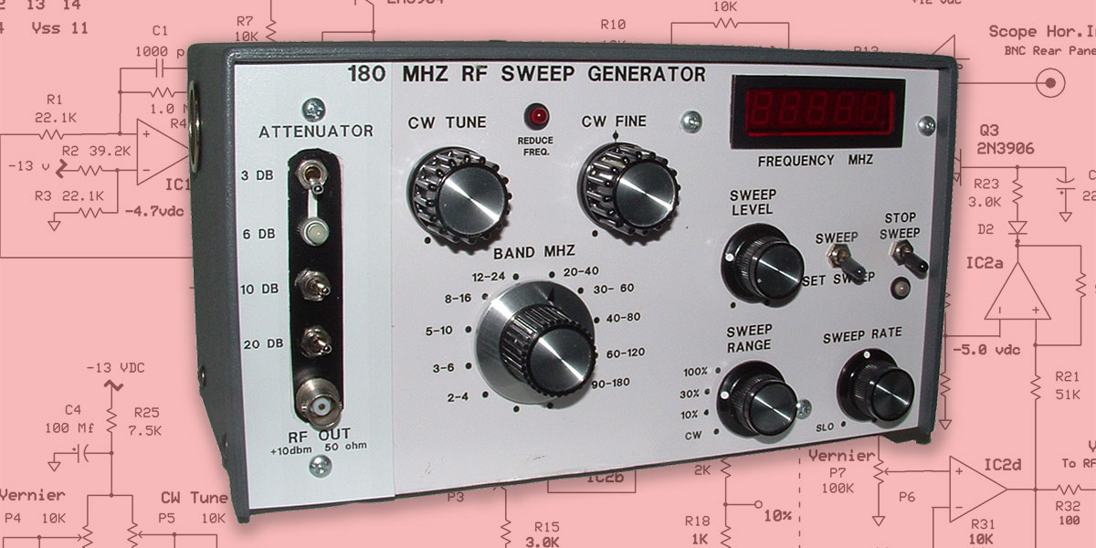
Sweep generators have a lot of uses in the design, prototyping, and troubleshooting of amplifiers, filters, and radio circuitry. They can greatly speed up these tasks by presenting many parameters at one time. The unit I’ll discuss here was designed and built to fulfill my needs to do just that.
For starters, I would like to emphasize that this is a low budget generator — not a $10,000 Agilent model — so a lot of concessions had to be made. In spite of that, this unit does a pretty decent job for general test bench use. I built it for about $50 in parts. Most of the common components came out of my junk box, but putting that aside you can still build it for around $100, less the enclosure (I built mine from some scraps of steel and aluminum sheet material).
Before I get into the theory of operation, I would like to discuss the background that led up to this arrangement. All of my designs were based on voltage controlled oscillators (VCO). Since it is difficult to get more than one octave of tuning range with the varactor diodes used in these circuits and still maintain fairly linear tuning, I decided that one octave would be my tuning range spec.
Since I use my function generator for all low frequency work (<2 MHz), I wanted a range of 2 MHz to upwards of 200 MHz of tuning. This would require a range of 100:1 — far more than a VCO could ever achieve. The only way to attain this range in one octave is to move it up into the VHF spectrum and then convert it down.
After doing some math, the optimum VCO would cover 300 to 500 MHz — a span that was easily obtainable, but also the start of a more expensive and complex device than originally planned.
The VCO signals would be fed into a mixer, along with a signal from a stable 300 MHz crystal oscillator. This produces (among other signals) a desired signal of fractional MHz to 200 MHz that could be made in one sweep. This had to be followed by a 200 MHz multipole steep sided low pass filter to reject any spurious signals that were produced in the mixer’s heterodyne process.
Along the way, attenuator pads had to be installed: one 10 dB pad between the mixer and low pass filter to “eat up” all the reflected energy that was above the filter’s pass band (these would have returned to the mixer in full strength, causing even more spurios heterodyne signal products); and another 6 dB mixer loss pad on the output to match it to a 50 ohm source, coupled with a 6 dB mixer loss. Quite a bit of amplification was necessary to make up for the losses. You probably can see where I am going with this, as circuit problems were beginning to mount.
The unit performance was fair, but had serious flaws that could not be easily or cheaply overcome. Firstly, frequency stability was less than desirable. Secondly, tuning was very difficult to accomplish due to the high ratio of output frequency vs. tuning voltage.
To make this picture clearer, consider a VCO that tunes 100 MHz with a Vt (tuning voltage) of zero to 10 VDC. That’s 10 MHz of frequency change for every volt applied, or 10 Hz per uV. Given a normal noise voltage of 200 uV residing on the tuning line would result in a constant 2 kHz of jitter — before you even touched a front panel control.
But wait! It gets even worse. For wideband sweeping in the upper frequency range, the sweep tuning was somewhat acceptable, but let’s say we wanted to look at tight 455 kHz or 10.7 MHz IF filters in the lower frequency ranges using a suitable sweep width for these frequencies (100 kHz and 500 kHz, respectively). The setup became impossible. Just merely breathing on any controls and the tuning varied wildly and erratically. It was so sensitive that it was impossible to tune and completely useless on the lower end or any narrow band of spectrum anywhere else for that matter. It was at that point I decided to abolish this design. A new circuit was “born.”
The new design breaks up the 180 MHz sweep into many one octave bands that offer satisfactory stability and tuning sensitivity to pick out any band of frequency and hone in on it precisely. This design uses 10 positions of a 12-position band switch — each position having generous overlapping bands of one octave. Due to its exceptional flatness of output, the switch can cover the whole spectrum almost as rapidly as turning a potentiometer. During this run-through, switching is stopped at points of interest and adjusted for closer observation.
Theory of Operation

FIGURE 1. RF deck.
Referring to Figure 1, the heart of this generator is the RF deck; it is based on a wonderful chip Motorola developed in the 1970s: the MC1648 — an ECL oscillator chip in a 14 DIP package with built-in automatic gain control (AGC). In fact, it has proven so popular it is still in current production, although these days it comes in a surface-mount package and goes under the name of MC100EL1648. These chips have a pinout for external LC components tied to the oscillator section, but just “beg” for varactor tuning in place of a fixed capacitance. They are well-suited for VCO design from 100 kHz to well over 200 MHz (the SMD unit will work up to 1 GHz). The AGC works very well over a wide range of LC ratios and tank circuit ‘Q’s, but does have its limits.
For those of you that do not know, varactors are special diodes that use a reverse DC across their junction to vary the junction capacitance. The higher the reverse voltage, the lower the junction capacitance. This design uses hyperabrubt diodes which generally produce the highest tuning ratio and best linearity, making them well suited for the tank circuit’s capacitance in wideband VCO use.
Starting with the MC1648, the frequency of oscillation is determined by the inductor selected (band switch) and the capacitance of the varactors junction as set by the tuning voltage controls. The varactor tuning network of VD1 and VD2 gives the optimum tuning range and capacitance for a wide assortment of complimentary inductors to cover a 0-180 MHz spectrum. Tuning voltage is supplied by the sweep circuit through R12. The resonating inductance is selected via S1A — a continuous rotating 12-position wafer switch.
This switch requires a small modification which is the installation of an RF ground plate to its rear end (see under Construction). This is necessary due to the fact that pins 10 and 12 (A and B) have a +1.6 VDC bias on them. For this reason, the low end of the tank circuit cannot return directly to ground, but still must be maintained at RF ground potential via C15, C16, and C17. This is a “digitized” combination of capacitors (rather than a traditional 0.1 mf cap) that provides better RF grounding across a wide range of frequencies.
The RF ground plate also facilitates coil installation on the band switch. The RF ground plate must be returned to the MC1648 P10 by a lead connecting it to point B as shown in the lower center area of Figure 1. A ferrite bead (FB1) is added to this line to insure no RF is present on it.
Q1 provides a high impedance take-off point from the tank circuit, and R2 (known as a stopper resistor) keeps Q1 stable and prevents the possibility of spurious oscillation. Q2 and Q3 provide a generous amount of buffering and impedance transformation for driving the output amplifier MMIC-1. R9 gives a good 50 ohm match to the MMIC (microwave monolithic integrated circuit) amplifier input.
MMICs are wonderful little devices used as gain blocks with built-in 50 ohm input/output impedances. Their upside is high gain, high output, and wide frequency response (DC to > 4 GHz). The downside (at least for this application) is they require a relatively high voltage supply and consume a fair amount of power. I weighed these issues against a two-stage transistor amplifier fed from an eight volt supply, but for pure simplicity elected to go with this device.
The extra added 24 volt supply (transformer, filter, and regulator) takes up very little room and is quite cheap.
At this point and with all the circuit’s signal levels adjusted properly, the RF output jack will display a clean sine wave of +10 dBm (2,000 mV P-P) with exceptional flatness of ± 0.1 dB, all the way up to 80 MHz (bands 1-8). Bands 9 and 10 (the highest bands) wander slightly from that figure but are still at a respectable ± 0.7 dB. This is due to the fact that we are pushing the limits here by outputting a 100:1 frequency range while mandatorily using the same values of the tuning cap in its tank circuit.
For any given frequency of oscillation, there is an optimum L/C ratio. We are at the point of exceeding those limits as the Q of the tank circuit drops to a low value at the upper frequencies (i.e., we would desire less capacitance and more inductance on the higher ranges to maintain optimum Q, but the minimum capacitance is limited by VD1,2).
This circuit uses a range of 80 uH to 20 nH. A ratio of 4,000:1 and the tank Q varies considerably throughout the total frequency range, which affects the tank circuit’s RF amplitude — also putting a strain on the AGC to keep up with it. Between the MMIC amp and RF output jack, an attenuator is desired to gain some amount of output signal level control. However, commercial step attenuators are extremely expensive ($150-$1,200) and continuously variable ones are even harder to come by.
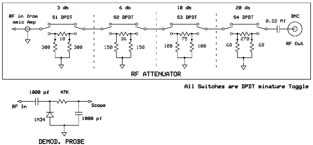
FIGURE 2. Attenuator and demod probe.
I decided to build a compromise attenuator (as shown in Figure 2) that would give 39 dB of attenuation (~100:1) and a resolution of about 3 dB increments, and yet still keep attenuator costs to an acceptable level. The four step attenuator filled this requirement and should be adequate for most testing.
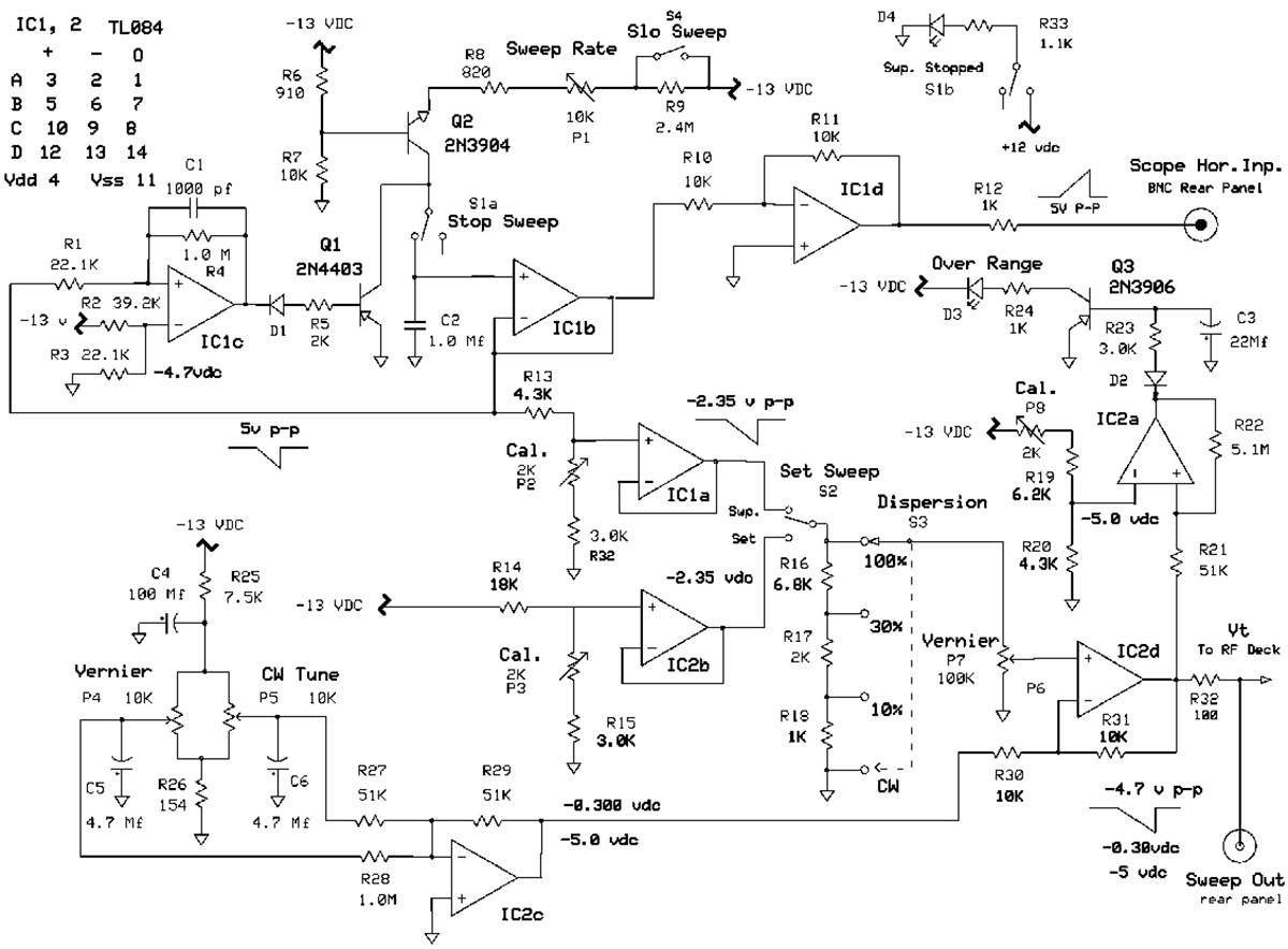
FIGURE 3. Sweep generator.
The sweep board shown in Figure 3 is where all the required VCO tuning voltages (Vt) are derived.
For use as a stand-alone CW (continuous wave) generator, the sweep portion is turned off by virtue of setting the Dispersion switch S2 to its CW position. Now, VCO tuning is done manually by the Main & Vernier tuning controls (P5 and P4). These are fed from the divider network of R25, R26, with a generous amount of filtering (we want this line to remain very quiet with respect to electrical noise).These controls output a DC voltage of -0.3 to -5.0 volts, and are also used to set the sweep start frequency when entering ‘sweep mode.’
Actual sweep voltage is derived from a very linear ramp voltage produced across C2 and fed to the input buffer IC1B. The ramp is generated by a constant current source (Q2) feeding C2. The rate of that ramp is controlled by R8 and P1 — about 10 Hz to 100 Hz.
Opening S4 (SloSweep) introduces R9 into the circuit, producing a very slow rate of 20 seconds (more on this later). Without further control, C2 would just keep charging until it reached -13 VDC and sit there forever, so it needs to be reset periodically; that is the job of IC1C and Q1. This is a comparator circuit set to trigger at approximately -5.5 VDC. The actual level is not that critical but repeatability of its trip point is hence the 1% metal film resistors used here — not for accuracy, but for stability.
R4 adds a small amount of hysteresis for noise rejection and consequent jitter. C1 is very important to hold the output reset voltage long enough (about 20 ms) to allow Q1 to completely dump the charge on C2, and then the whole charging process repeats itself. IC1B’s output feeds off in two different directions: an inverting amp (IC1D) with a gain of one to drive an oscilloscope’s horizontal or ‘X’ axis; and the other to a calibration pot (P2) for setting the exact amplitude of the ramp voltage into IC1A. IC2B outputs a DC voltage of the exact level that matches the peak amplitude of the ramp voltage coming out of IC1A. This level is calibrated by P3.
The Set Sweep switch (S2) is used for setting the sweep stop or end of sweep frequency (more on this later). With S2 in the sweep position, the ramp voltage is fed to S3 — a four-position range switch to allow coarse adjustment of the sweep or frequency dispersion. P7 is the fine adjustment of the range selected, and feeds IC2D.
As mentioned earlier, CW tune and Vernier are for manual tuning or sweep start frequency. These two control voltages are summed in IC2C and fed to IC2D where they are summed with the ramp voltage. That output (Vt) is then sent to the VCO on the RF deck for biasing the varactors. The output of IC2D has an intended range of -5.0 volts; more specifically, -0.3 to - 5.0 volts to manually tune one complete octave for the band selected. Its output may also contain a ramp voltage of 0 to -4.7 P-P.
When a -4.7 volt ramp is added to the minimum CW voltage of 0.3 volts, we have a range of -0.3 to -5.0 volts — exactly the same as the manual tuning voltage range and the optimum tuning voltage range required by the VCO. So, we can sum any combination of CW and ramp voltage that will stay within that -0.3 to -5.0 voltage range. Since (obviously) we could easily sum both of them to a level that would not only drive the VCO out of its linear range but also drive IC2D into saturation (producing a flat spot on the sweep ramp and giving erroneous readings on a CRT trace), this is a no-no! So, how would we ever be aware this is happening?
That is the job of comparator IC2A to warn us of this situation. Its trip point is set for about -5.2 volts. When this level is reached, the trip level drives Q3 into saturation which, in turn, lights D3 (labeled ‘Reduce Freq’ on the front panel). You’ll see a slow flashing at first, then a constant on. Since the very peaks of the ramp in the tripping mode are of such short duration, they would not hold the comparator on long enough to see any visible light from D3. Capacitor C3 was added to give adequate hold time for these short duration trips.
The calibration pot P8 sets the level of the trip point. One feature I added that is optional is the ‘Stop Sweep’ Alert LED D4 at the upper right of Figure 3. The original Stop Sweep switch was changed from an SPST to a DPDT (S1A and S1B) with an LED added to the second pole. Now when the sweep is stopped, the LED lights up and alerts me to this.
There were times (that for the life of me) I couldn’t figure out why the generator was not working properly, when it would finally dawn on me that the sweep was in the stopped position. Now, the LED alerts me to that situation every time. The Stop Sweep switch S1A is used in conjunction with the SloSweep switch S4 for marking frequency. I used this method rather than a traditional marker generator which adds a lot more circuitry, expense, and sometimes a lot of confusion. More on this later.
The generator’s final specifications are shown in Table 1.
| Frequency Span |
2 MHz to 180 MHz in 10 bands with a 25/30% overlap. |
| Frequency Stability |
Better than 200 ppm after warm-up. |
| RF Output |
+10 dBm (2,000 mV P-P) of clean sine wave into 50 ohm termination. |
| Output Flatness |
± 0.1 dB 2 MHz to 80 MHz ; ± 0.7 dB 70 MHz to 180 MHz; 50 ohm term. |
| Attenuation |
39 dB (approx. 100:1) in 3 dB steps. |
| Sweep Linearity |
@ 100% sweep <1-2 % error @ 10 % sweep < 0.2 % error |
Table 1.
Construction
I built the internals in three separate modules so that each could be separately tested before installing in the chassis: the RF deck, sweep board, and power supply. The RF deck was built on a 2” x 2.5” single-sided circuit board in typical RF prototype fashion. Figures 4 and 5 show the bottom and top views, respectively.
First, I draw out all the components on a sheet of quadrille graph paper with each intersection representing 0.1” spacing. All components are included — both top and bottom mounted. These are drawn as you view the top of the board, but also using ‘X-ray’ vision to see the bottom (copper side) of the board.
After completing the layout on graph paper, the hole locations are transferred to a scrap of perf board of the same dimensions as the actual circuit board and held in place with double-sided tape. This also makes a nice drilling guide for a clean appearance. Ideally, use a #56 drill (0.040”), but lacking that you could go as large as 1/16”.
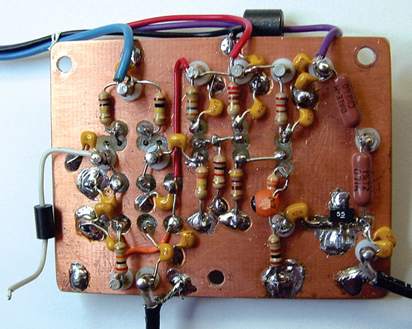
FIGURE 4. RF deck — bottom view.
After drilling is completed, clean out the copper side of the holes for components that do not go directly to ground by hand spinning a larger drill bit. This opens up the copper foil to give adequate insulation around it; about 1/8” is sufficient. Figure 4 gives you a general layout scheme.
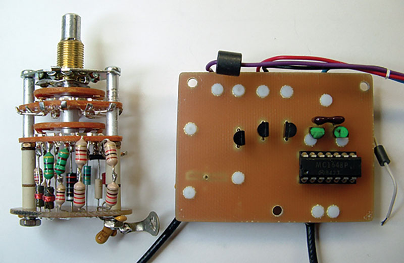
FIGURE 5. RF deck and band switch — top view.
After the active through-hole components are inserted, their leads are used as solder tie points. All other circuit nodes above ground are soldered to insulated standoffs (the white dots in Figure 5) and, of course, the grounded components are soldered directly to the ground plane. The layout is pretty straightforward and follows the signal flow as shown back in Figure 1.
If you have never worked with RF frequencies before, two rules are paramount. First, a ground plane type of construction as used here is mandatory; the other is to keep component leads as short as possible. There is an old saying among RF design engineers: “If you can see the leads, they are too long.”
A few other things to mention are the MMIC amplifier is an SMD device and is located in the lower right of Figure 4. It required two “islands” to be ground out for its input and output terminals; these were the only islands needed on this board. The other is that two insulated standoffs were mounted close to the MC1648 P10 and P12 connections (A and B). This is for connecting to the band switch which will eventually end up sitting right over the top of them. They are located in the middle left of Figure 4 and are a little hard to see. Pin 10 already has its lead installed with a ferrite bead in place.
Lastly, the MV1404 varactor diodes I used in this particular project came in TO-92 packages which are becoming very hard to find. They were later replaced with an MV 1404-9 which is a dual diode unit in a single SMD package. It also improved performance slightly.
The 12-position band switch shown in Figure 5 is made up of a two-pole, double-deck 12-position wafer switch.
The first deck is used for AGC level resistors. Cut a piece of single-sided circuit board a little larger than the size and shape of the switch deck. Drill two mounting holes for attaching to the switch bolts and ream out the copper side to provide an insulating barrier. Drill 12 small holes in a slightly larger circle pattern than the switch contact points. Remove the switch bolts one at a time and replace with 2.5 mm x 2” screws (4-40 thread will work but requires a small amount of reaming to pass through).
Nut these down to the switch, then install two spacers of approximately 1” length on the protruding bolts. Install the previously made up circuit board with the copper side to the rear. Drop a couple of insulating washers over the bolts and nut down the assembly firmly (don’t go crazy here). This newly added circuit board is the RF ground plate shown as such in the schematic.
The coils are mounted by shoving one lead through the ground plate hole and then cutting the other lead to length; merely lay it on its associated switch lug and solder. Solder the end protruding through the ground plate and trim off the excess. Then, continue to the next one until finished.
Installing band’s 9 and 10 coils adjacent to the wiper contacts will alleviate some of the switch’s parasitic reactance which becomes more dominant at these higher frequencies. The chart in Table 2 shows the band and associated coil value.
| Band 1 |
2 - 4 MHz |
80 uH |
Band 3 |
5 - 10 MHz |
12 uH |
| Band 2 |
3 - 6 MHz |
33 uH |
Band 4 |
8 - 16 MHz |
4.7 uH |
| Band 5 |
12 - 24 MHz |
2.2 uH |
Band 8 |
40 - 80 MHz |
0.18 uH |
| Band 6 |
20 - 40 MHz |
0.82 uH |
Band 9 |
60 -120 MHz |
65 nH |
| Band 7 |
30 - 60 MHz |
0.37 uH |
Band 10 |
90 - 180 MHz |
20 nH |
Table 2.
Given the tolerance on these coils, the labeled band frequencies are very nominal but will be in the ball park for a guide. All bands have sufficient overlap so that no voids will occur. (Some of these coil’s values may be unobtainable due to being out of stock or on back order, but they can be made up in series with other values — just add up values in the same way as series resistance.)
Solder a piece of #22 solid hookup wire about 3/4” long to the wiper contact. Now when this switch is installed, that lead will be at the bottom of the switch and positioned directly over the area of the MC1648 P12 or stand-off. Note that the RF deck is mounted upside down and directly under the band switch. This switch is mounted 1-1/4” (shaft center) above the Rf circuit board surface.
You can panel mount it, or do as I did and mount the RF deck and switch to a scrap of 1/32” aluminum bent at a 90 degree angle. This can then be powered up for basic checkout before the whole sub assembly is installed in the enclosure. This method facilitates checkout as a stand-alone sub assembly and was mandatory in my case for the design process. The sweep circuit was built on a RadioShack 276-168B circuit board. I love these little boards as they accept DIP devices very nicely. The board measures 2-1/4” x 2-1/2”. Layout is straightforward and non-critical; although, I added a 16-pin header due to a multitude of lead connections to the front panel controls. Also, do not use a ceramic capacitor for C2 — mylar is best!
Generally, I only take a circuit’s power requirements back to the voltage and current requirements needed, and leave it up to the builder to rummage through their junk box for the parts necessary to complete the raw voltage supply. Since this project includes an odd assortment of voltages, I am including a schematic for it. The circuit is so simple and straightforward that no explanation is really needed here. Hence, no parts list was written up for it. However, the transformers will appear in the overall parts list, and they are quite small and cheap.
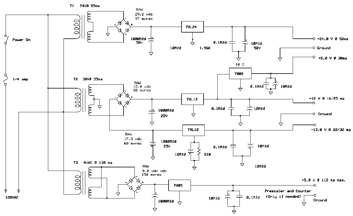
Power Supply.
Also, you may be wondering about the -13V supply. I wanted a ±12V supply for the op-amps. The negative supply is used as a reference voltage at many points on the sweep generator board (Figure 3). Since the 79L12 can vary by almost a volt either way in tolerance, I wanted to make sure I had a specific voltage at this point. This simplified the design and will always insure that it can maintain that voltage — even if replacement of that regulator was required. The regulator voltage can be adjusted up by virtue of its common pin resistor, but you can never make it lower. So, by adding resistance to that pin, a -13V output will always be obtainable — no matter what the regulator’s tolerance is. The 79L12 I used required a 510 ohm resistor to output exactly -13.0V. The 79L12 you use may have a different tolerance and will require a different value. Shoot for 1% of the target voltage — not difficult to do. The attenuator is shown in Figures 2 and 6.
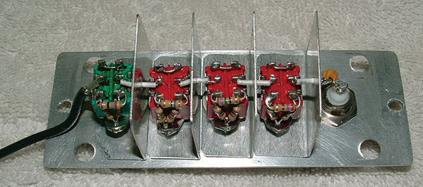
FIGURE 6. Attenuator.
As you can see in the photo, I built mine on a shielded panel that gets enclosed in a box. This was probably overkill as 40 dB of attenuation is not that great. I think the switches could merely be panel mounted and spaced on 5/8” centers without any shielding and perform just fine. These use garden variety miniature toggle switches and 5% 1/4 watt resistors. I have had decent performance in the past with this type of construction in upwards of 200 MHz frequency. This one checked out with a worst case error of 3%. Note that the top two attenuator switches shown on the front panel look a little odd. This was a temporary change I made to facilitate a battery of repetitive tests I am making, and normally these would be side to side toggles as the lower two are.
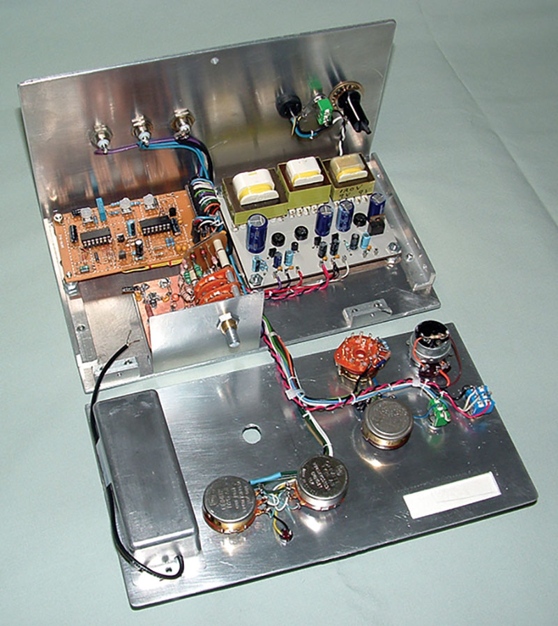
FIGURE 7. Internals.
Figure 7 shows the internals and can guide you as to overall layout. I built the chassis by forming a 90 degree bend in a piece of 1/8” aluminum sheet stock. Four 3/4” aluminum L brackets were cut and mounted to this piece for attaching the front panel and cover. The front panel was cut from 1/16” aluminum sheet and fastened to the two front brackets with two 6-32 screws. The cover was a piece of 20 gauge steel sheet with two 90 degree bends that was attached to the side brackets with four 6-32 screws.
The front panel layout points and artwork were made using a free program from Front Panel Express (www.frontpanelexpress.com). See my power supply article for more detailed info on these procedures.
Calibration and Usage
For the following tests and procedures, an oscilloscope and frequency counter are required. Starting with the RF deck, ideally you will want three voltages to coincide with those shown in Figure 1. Since Q1, Q2, and Q3 are DC coupled, the DC current through R4 sets these levels. You want to be as close to 2.3 VDC here as possible by selection of the value of R1. This could be quickly done on a solderless breadboard with the intended transistor used.
The next point to check is the signal level at the Q2 emitter. This should be within 5% of the 370 mV P-P value as shown back in Figure 1. Minor changes in R13-R17 (AGC) will set this if necessary for those particular bands.
Finally, the signal level at the C11, R9 junction should be 185 mV P-P. Make these tests at 2 MHz with your scope’s 10:1 probe. If all levels are correct, you should see 2,000 mV P-P at the RF output jack with no attenuators switched in and terminated in 50 ohms. The MMIC’s gain is about 21 dB.
On to the sweep board. Attach a DMM to the output of IC2B (S2 throw) and adjust P3 (DC calibration pot) for exactly -2.35 VDC. Display that level on one channel of a properly calibrated oscilloscope. On the other channel, display the ramp voltage from the output of IC1A (the other throw of S2). Adjust P2 (ramp calibration pot) so that the P-P ramp level exactly matches the -2.35 VDC level.
Now, the Set Sweep switch compares a DC voltage to the ramp’s peak amplitude regardless of the adjustment of Dispersion switch (S3) or Dispersion level (P7). This allows for a stable frequency reading when setting the dispersion or sweep stop point frequency. When the Set Sweep switch is flipped back to its sweep position, the ramp’s peak will always equal that DC set point and consequently sweep the frequency to that exact setting.
Remove the scope probes and attach one probe to the output of IC2D. Adjust CW main to obtain two or three volts DC here, then turn up the ramp amplitude until the combination of the two equals -5.0 volts at the ramp’s negative peak. Adjust calibration pot P8 until LED D3 just starts to flash. This is the alert signal of exceeding the maximum range of linear tuning voltage. This completes calibration.
At this point, a brief explanation of the front panel controls is in order. With the Dispersion switch (S3) set at its CW position, the Main Tune control will manually tune one octave of frequency for any band selected. This allows the unit to be used as a common CW signal generator. The Vernier tuner (P4) which normally sits at its midpoint position allows a ±2% shift for fine adjustment.
In Sweep mode, the Start Sweep frequency is adjusted as just explained. Switch the Dispersion Range (S3) to an applicable position and S2 to the Set Sweep position and adjust the Dispersion level (P7) to the desired sweep upper limit frequency. Any value of zero to one octave of sweep can be achieved, depending on the start and stop frequency adjusted by these controls.
Place S2 back in Sweep for sweep operation. The Sweep Rate control (P1) will allow sweep rates of 10 to 100 Hz, and is adjusted for the best CRT presentation. Normally, the faster rates are desired, but for tight filters it will have to be slowed to reduce distortion. The SloSweep mode switch S4 (mine is attached to P1) is used in conjunction with the Stop Sweep switch. This produces a slow moving dot across the CRT screen that can be stopped at any point by operation of S1. This effectively makes IC1B a sample and hold circuit, and will maintain that dot position for several minutes before any noticeable movement of that dot occurs.
In actual testing, impedance matching will insure accurate results, but if the input and output to the device under test (DUT) have adequate isolation then a decent test can be accomplished. Two example tests may make the usage a little clearer:
Example 1 — To test the resonant frequency of an 8.5 MHz parallel resonant circuit, set the generator to full sweep at 5-10 MHz (band 3). Feed a signal into the DUT of the desired level through adequate isolation. Connect the scope’s vertical input probe to the output of the DUT. Connect the scope’s horizontal input to the Scope Horizontal jack from the generator and adjust for exactly 10 graticules of trace. We are now sweeping at 500 kHz per graticule division (5 MHz/10 divisions).
You will see a definite peak in voltage as the trace travels across the screen. Let’s say it peaked at seven graticule divisions; the resonant frequency is 8.5 MHz (sweep start frequency at 5 MHz plus seven divisions at 500 kHz per division). The sweep rate can be slowed to 20 seconds with S4 (at this point, the horizontal trace will be a slow moving dot rather than a solid line), and the moving dot will stop right at its peak with the Stop Sweep switch (S1A) and the exact frequency read from the Counter Output jack.
Similarly, the dot can be stopped at the -3 dB point (bandwidth) or any unusual aberrations for marking frequency. The dot may be stopped anywhere along the horizontal axis to mark frequency.
Example 2 — You may want to check out the frequency response of the wideband amplifier you just prototyped. Start with the lowest band at 100% sweep and just rotate the band switch as you would a potentiometer. Stop at the -3 dB point, also noting any unusual events along the way. You can go to SloSweep to mark the frequency at any points of interest.
Due to the generator’s exceptional flatness of amplitude, switching through the bands always maintains the same input level for accurate test results. At first, these controls and their interactions may seem a overwhelming but I guarantee you that after a few hours of playing with them on the test bench, they will become “old hat.”
Closing Notes
The above test examples were very basic just to familiarize users with the operation of this generator, but far more involved tests really will make a sweep generator appreciated as to its ability to gather info in a short amount of time. That part I will leave to the builder to gain more knowledge from the Internet and other sources.
I wish I had more space to go into more detail on all the different aspects of this project, but since I don’t, I have included some websites after the Parts List that contain a wealth of information.
So, there you have it. There are a lot of variables here. You can build this generator exactly as described or add bands (two vacant switch positions are still available), delete bands, or even hopscotch bands that suit your particular interests. Or, maybe just use the RF deck or sweep board to adapt into different designs of your own.
RF loves surface-mount technology. So if you are into this, all the parts are available in SMD packages (of course, the MMIC amplifier and varactor diode already are).
I have also included a schematic of a detector probe back in Figure 2 that can be used to give an envelope display rather than an RF presentation on the CRT. However, it requires a high level of detection for good linearity. Fair linearity can be obtained in the 100-1,000 mV range. I did add ventilation holes in the enclosure so that the unit reaches thermal equilibrium in a shorter time period. Future plans call for an active detector probe so as to drive the detector diode at a higher level for improved detection linearity.
The completed generator is shown with its own internal frequency counter and prescaler, but these were omitted in the internals picture of Figure 7 for clarity (although I kept the optional supply in the power supply schematic). Unfortunately, space does not permit for that construction since it would be a complete article in itself. If there’s enough interest, the editors may be open for a follow-up article on the design and construction of that. NV
PARTS LIST
| All resistors are 1/4 watt 5% unless otherwise noted. *Asterisks denote 1/4W 1% metal film. |
| RF Deck: |
| R1 |
150K |
| R2 |
390 ohm |
| R3 |
150 ohm |
| R4 |
1K |
| R5 |
220 ohm |
| R6 |
470 ohm |
| R7 |
120 ohm |
| R8 |
240 ohm |
| R9 |
43 ohm |
| R10, R11 |
* 200 ohm 1 watt Vishay-Dale CMF60200R00HEK |
| |
| C1-C2, C4-C10, C12, C14, C16, C18 |
0.1 mfd |
| C3, C17 |
0.01 mfd |
| C11 |
0.22 mfd |
| C13 |
0.47 mfd |
| C15 tantalum |
4.7 mfd |
| |
| FB1 |
J.W. Miller |
FB43-226-RC |
| FB2 |
J.W. Miller |
FB43-287-RC |
| L1-L10 |
See text chart for values. Conformally Coated, Fastron, or Xicon |
| |
| U1 |
(14 DIP) |
MC1648 |
| U1 (alternate.) |
MC100EL 1648 |
(SMD) |
| MMIC |
Mini Circuits |
GALI-55 |
| Q1 |
2N5179 |
| Q2, Q3 |
2N3904 |
| VD 1,2 |
MV1404-9 (varactor diode) |
| RF Band Switch (S1) |
Alpha SR2921F-12S |
| Alpha also carries a line of low priced potentiometers used in this project. |
| Sweep Generator Board: |
| R1, R3 |
*22.1K |
R26 |
150 ohm |
| R2 |
*39.2K |
R32 |
100 ohm |
| R4, R28 |
1.0 meg |
R33 |
1.1K |
| R5, R17 |
2K |
|
|
| R6 |
910 ohm |
C1 |
-0.001 mfd |
| R7, R10, R11, R30, R31 |
10K |
C2 |
1.0 mfd Not ceramic or 'lytic |
| R8 |
820 ohm |
C3 |
22 mfd 'lytic |
| R9 |
2.4 meg |
C4 |
100 mfd 'lytic |
| R12, R18, R24 |
1K |
C5, C7 |
4.7 mfd tantalum |
| R13, R20 |
4.3K |
|
|
| R14 |
18K |
D1, D2 |
1N914 |
| R15, R23 |
3.0K |
D3 |
10 mA LED red |
| R16 |
6.8K |
D4 |
10 mA LED amber |
| R19 |
6.2K |
Q1 |
2N4403 |
| R21, R27, R29 |
51K |
Q2 |
2N3904 |
| R22 |
5.1M |
Q3 |
2N3906 |
| R25 |
7.5K |
IC1, IC2 |
TLO84 |
| Power Supply |
| T1 |
120V/24V c.t. @ 85 mA SB3512-2024 |
| T2 |
120V/30V c.t. @ 55 mA SB3518-3030 |
| T3 |
120V/18V c.t. @ 65 mA SB2812-2018 |
- MC1648 and MC100E 1648 datasheets are easily obtained through Google and have a lot of good information. DIP version available at www.elexp.com (Electronix Express). Most major distributors carry the MC100EL1648.
- MMIC-1 is available at www.minicircuits.com. Ordering can be done directly. Also, lots of downloads for info.
- MV1404-9* is available through Arrow Electronics. Datasheets are on the Web.
- Band switch S1 available at Mouser (Mouser# 105 prefix). Also the line of Alpha pots are quite cheap here.
- Coils L1-L10 and ferrite beads available at Mouser and Digi-Key.
- Tamura transformers T1, T2, T3 available at Mouser and Digi-Key (Mouser #838 Prefix).
- All catalog nos. are Mouser.
- *MV1404 - 9 is subject to availability.