Good Things Come With Small Packages
By Bryan Bergeron
If we’re talking about a $5 device, then the practical solution is to simply buy a new one. But sometimes there are impractical issues involved: the challenge of diagnosing and repairing a piece of electronics; the sentimental value of a device; or the need to validate your expertise in electronics to others. Whatever the reason, if you’re faced with the task of repairing the circuit, don’t forget to leverage the signposts staring you in the face — namely the component packaging.
Fortunately, many leaded and SMT components use standard packaging. For example, in the diagram, you can see that SMT transistors in the Small Outline Transistor (SOT)-23 packaging have standard lead designations. Facing the top of the package (with the single lead on top), the base lead is in the lower left lead; the emitter is the right lower lead. The collector is the lone top lead.
If you need more information — such as whether the device is PNP or NPN — it’s a simple matter of using your ohmmeter to identify the polarity of the individual junctions. Recall that with an NPN transistor, the emitter-base junction conducts when the emitter is negative, relative to the base. Alternatively, you can monitor the voltages on each lead, looking for forward and reverse bias conditions to identify transistor types.
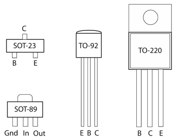
The SOT-89 package is often used with voltage regulators. As shown in the figure, ground (Gnd), input (In), and output (Out) are standard leads, from left to right. The tab on top is connected to the input lead. It’s a simple matter to check the voltage input and voltages of the device to help determine whether it’s working. If there’s no output with an input, then the component may have failed or there may be a short in the output circuit. Many voltage regulators are short proof.
The same diagnostic walkthrough applies to transistors in leaded TO-92 and TO-220 packaging. Armed with lead designation and transistor type, a board full of components suddenly takes on new meaning. You should be able to sketch out a simplified schematic and have a good idea the area of the board responsible for the failure. All is not rosy in the land of SMT components, and there are some formidable challenges associated with the latest SMT devices, namely lack of markings because there simply isn’t space on the device to write anything legible. As it is, I’m forced to rely on a 10X scope when I work with a board populated with SMT components.
Another challenge of working with SMT components is simply getting a probe on a specific lead without short-circuiting the device. To this end, I recently picked up a pair of needle-tipped probes by Fluke on eBay. I’m dreading the day when I impale myself with one of the probes, but they allow me to make measurements of SMT components that would have been impossible with standard leads.
Assuming you’re successful in identifying the defective transistor or other component(s), the next step is to replace the component. For this, I rely on Digi-Key ([url=http://www.digikey.com]http://www.digikey.com[/url]) and Mouser Electronics ([url=http://www.mouser.com]http://www.mouser.com[/url]). A short blast of air from a hot air pencil removes the defective component from the board. If you prefer, a standard soldering iron with solder wick works just about as well.
Taking the time for shipping the replacement components into account, give yourself about a week to repair anything substantial. Not bad, when you consider most electronics devices are simply tossed in the trash at the first sign of trouble — to the detriment of the environment. NV
Comments