In 1984, Forrest Mims wrote a very popular booklet published by RadioShack: Mini-Notebook 555 Circuits. It contains 28 circuits using either a 555 or 556. All of the circuits are relatively simple, but they do form a very good basis for learning how to use the 555/556. The following article is the first of several which will detail the emulation of a 555 or 556 using a PIC. This particular implementation does both the monostable and astable modes, and is meant to be used only as a 555 or 556 emulator. Future articles will discuss the software needed to share the PIC's resources so that the emulation can be embedded within another application.
PIC Based Enhanced 555
Since I retired in 2012, I have been volunteering technical assistance at a network of FM radio stations throughout the state. One of the issues they have had is that a device they use at several remote transmitter sites does not connect to the Internet router properly after a power outage. The station manager asked me if there was anything I could design that would help.
What I needed to build was basically a delayed one shot where the delay is retriggerable. The operation is such that if the audio stream coming from the target unit stops for some period of time, it will reset the unit.
The circuit and software I developed led me to this project: an “enhanced” multivibrator which I have used as a 555 replacement.
The features of the software are eight decades of time resolution, from 1 µs (range = 0) to 10 seconds (range = 7); each range has a span of 10 bits. For example, the 1 ms range spans from 1 ms to 1,023 ms in 1 ms steps.
Also, there are currently six operating modes:
- One shot monostable multivibrator
- Delayed one shot
- Retriggerable one shot
- Delayed and retriggerable one shot — both delay and pulse width are retriggerable
- Astable multivibrator with separate control of both the on-time and the off-time
- Same as 5, but with a synchronous gate
All of this is accomplished without having to re-program the PIC in any way. The only “programming” needed is to configure the PIC using up to four resistor dividers. By changing some definitions in the source code, the analog inputs may be swapped. However, RA3 and RA5 must be kept as shown.
RA3 (pin 4) has special internal handling due to its possible usage as the MCLR/VPP input. Its only other allowed use is as a digital input. RA5 cannot be used as an analog input. Due to the different pin functions, there is no way to make the device pin compatible with a 555. One obvious reason is that the 555 has ground on pin 1 and VDD on pin 8 — just the opposite of the PIC12F1572 I used.
The software is written so that both the mode and range values are read only once — at program startup. The pulse width and delay/off-time may be read before each pulse is generated.
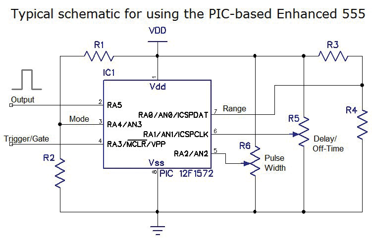
FIGURE 1.
Some of the advantages of this implementation as compared to a 555 or 556 are:
- No capacitors
- Very linear response for pulse width
- Delayed pulse capability independent of the pulse width
- Independent control of pulse width and off-time in astable operation
- Very wide range of pulse width and off-time/delay
- Output pulse width is independent of the triggering pulse width
Some disadvantages:
- Shortest trigger to output delay is about 1 µs
- Shortest pulse is about 3.3 µs
- Longer minimum time between triggers due to reading the ADC (analog-to-digital converter) and other processing
- Pulse width and delay use the same range
Some advantages of the 555:
- Lower cost
- Very low delay time between the trigger and the output pulse
- Narrower pulses possible: <500 ns
As of this writing, these are the approximate prices for single pieces:
PIC12F1572 (DIP and SOIC) = $0.60
NE555PSR (SOIC) = $0.37
NE556DR (DIP) = $0.45
CSS555 (SOIC) = $1.55
Both the range and mode of operation have up to eight values. The operating values are determined by using the upper three bits of an analog voltage for each. The resistor network shown in Figure 2 is an example of how to develop the voltages required for setting them.
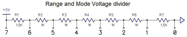
FIGURE 2.
The voltage shown is for example only — you would never use +8V for the top of the divider! With the values shown, the divider draws 1 mA and the taps are 1V apart starting with 1.5V at tap 1.
The ADC in the PICs is ratiometric: The digitized value is the ratio of the applied voltage to the difference between the high and low references; it’s then multiplied by 2N, where N is the number of bits of the ADC. The references typically used are VDD and ground (the PIC12F1572 does not allow a choice for the negative reference). For this project, the formula is:
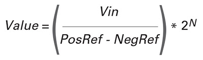
Using 8V for the positive reference, ground for the negative reference, and N = 10 for the 10-bit ADC, the formula reduces to:

For example: if Vin = 4V, I would expect the ADC to show a value of 1/2 full scale. Using the formula: Value = 4 * 128 = 512, which is 1/2 of full scale for a 10-bit ADC.
For this project, the program uses only the most significant three bits of the converted value for the range and mode inputs. The voltage divider is designed so that the six taps are exactly centered on the voltages needed for each of the six intermediate values. The voltages for the range and mode 0 and 7 use ground and VDD, respectively, and do not need a divider. Using range 2 as an example, the voltage at tap 2 is 2.5V. The converted value (using the formula) is 2.5 * 128 = 320.
The 10-bit binary value of 320 is 01 0100 0000. As you can see, the upper three bits (bits 9-7), 010, are the value 2. Any value between 01 0000 0000 (256) and 01 0111 1111 (383) will also work. This yields a window of 127 or — with a 5V power supply — about 620 mV. By selecting the divider as I have, you can see that the voltage tap is centered in the window and yields the best solution, taking into account noise and circuit tolerances.
Since the ADC is ratiometric, the actual value of the positive reference is not relevant (keeping within the specifications of the PIC) as long as the input to the ADC does not exceed this value. The voltage divider resistors can stay the same as shown — also independent of the reference.
For a specific application, you may want to change the divider to only two or three resistors. For example, if you want range 3 and mode 1 (or range 1 and mode 3), the divider could be what you see in Figure 3.
FIGURE 3.
Notice that the total resistance is still 8K even though the positive reference is 5V. One parameter you need to take into consideration when selecting the resistor values is that the specifications for the ADC state that the maximum resistance of the source should be less than 10K ohms.
It is possible to extend this method beyond using only the upper three bits. Using the upper four bits will yield up to 16 possible “states.” This will cut the noise/tolerance range in half to 63 counts of the ADC, or about 310 mV.
Theoretically, this method could be extended to the full number of ADC bits, but I would hesitate using it beyond six bits (a 68 mV window) mainly due to noise and other circuit tolerances. Keep in mind that six bits is about 1.5%, so using 1% resistors in the divider would be absolutely necessary. Even then, you would want to verify the voltage values at each tap.
Some Program Specifics
In order to get the best resolution for the ranges, the program changes the CPU clock speed depending on the range selected, as follows:
Ranges 0-4: 32 MHz clock = 8 MHz instruction rate = 125 ns period
Range 5: 8 MHz clock = 2 MHz instruction rate = 500 ns period
Ranges 6 and 7: 2 MHz clock = 0.5 MHz instruction rate = 2 µs period
The initialization of the processor starts the CPU with the 32 MHz CPU clock. Running at 32 MHz requires the use of the internal PLL which takes about 1 ms to stabilize. If range 5 is selected, the program will decrease the CPU clock to 8 MHz. If range 6 or 7 is selected, the CPU frequency will be lowered to 2 MHz.
These frequencies were selected in order to meet my goal of eight decades of resolution. Also, keep in mind that the PIC processors have four cycle instructions; for instance, a 32 MHz clock results in an instruction time of 125 ns.
Range 0 uses a timing loop with eight instructions so that the time to execute the loop is 1 µs. Ranges 1 through 7 use timer 1 with a preset value read from a table in program space. For all ranges — except 0 — the timer 1 clock is derived from FCPU/4 with the prescaler value set to 8, which makes the timer 1 clock frequency = FCPU/32.
The ADC reading for the pulse width and delay/off-time is used in software timing loops which — for ranges 1-7 — determine the number of times timer 1 times out.
There are several configuration macros which have been implemented to help a user who may want to customize the program:
DEBUG: Defining this value to 1 reassigns several of the I/O pins so that you can use the PIC debugger.
FAST: Define this value to 1 to speed up some of the times by reading the ADC only once during start-up. This means that not only the mode and ranges but the pulse width and delay time will also be fixed once the start-up code has completed.
AD_NO_BITS_0_1: Defining this to 1 causes the ADC read function to clear bits 0 and 1 of the reading. This will make the pulse width and delay/off-time values less susceptible to noise, at the expense of reducing the resolution by a factor of four while maintaining the same full scale capability.
AD_USE_8_BITS: Defining this to 1 causes the ADC read function to use only the upper eight bits of the conversion. This is different from AD_NO_BITS_0_1 in that the resolution is unchanged, but the full scale capability of each range is reduced by a factor of four.
EDGE_REG: Define as IOCAP to trigger on positive edges; define as IOCAN to trigger on negative edges.
One of the ADC control registers is modified — based on the selected range — to make the sample time/bit 1 µs (called TAD in the specs) which makes the conversion time (plus some processing) about 18 µs. The delayed one shot and astable multivibrator modes read the ADC twice: once for the delay/off-time and once for the pulse width. For the astable multivibrator mode, the reading for each state is taken immediately preceding that state so that both states are lengthened by the same amount of time.
For the one shot modes, the ADC is read before the program looks for the trigger signal so the reading times do not affect the trigger-to-pulse delay. However, the reading time does affect the minimum time between triggers.
I considered using interrupts to handle the ADC readings. However, since the interrupt can occur at almost any time, it would eventually happen when the timing loop was to terminate, causing the pulse to be delayed longer or the pulse width to be a little longer. The effect would be that some pulses would be longer than others. I felt that having the timing be more consistent was the better solution.
Something I noticed on the several PIC12F1572s I was using is that the ADC seldom returns a value of 0; even with the input grounded, it almost always reads a value of 1. This causes the pulse width and delay/off-time values to be one count larger than you would expect with a grounded ADC input. I thought about decrementing the values just prior to entering the timing loops, but decided against it since this would affect all settings.
All of the processor’s “math” instructions operate on eight-bit values. However, it has auto-increment and auto-decrement instructions that use 16-bit pointers to access memory.
I decided to use one of these two registers as a 16-bit counter to contain the ADC value for the pulse width and delay. Even though this register accesses a memory location and copies it to the W register, I ignore it.
I use the auto-decrement mode each time through a loop and test the most significant bit. If it is on, the register has decremented to a negative value and the loop is terminated. Using this method saves three instructions which — in the case of 1 µs resolution — is significant. I did not need to use this method for the other ranges, but I chose to use it in order to be consistent.
The gated astable mode operates such that when the gate is enabled (high), the output pulse will be immediately generated. This will be followed by the off-time. The program will complete the entire cycle of pulse followed by off-time before it again looks for the gate.
The re-trigger pulse for the re-triggerable modes can happen any time during the cycle. The triggering edge of the re-trigger signal is captured by the processor and can be a very short pulse (>25 ns). If a re-trigger is detected, the current output cycle will be restarted. If the delayed one shot mode is selected, this means that both the delay time as well as the pulse width are re-triggerable. This is the mode I used in my application — as long as audio is present, it will re-trigger the delay time.
When audio stops for delay time seconds, the delay time will time out and a pulse will be generated. The pulse turns on a relay which removes power from the device for about 20 seconds and then re-applies power. The delay time must be long enough to allow the device to re-acquire the audio signal or the power-off cycle will repeat.
Some measurements for each of the ranges in mode 0 (one shot):
Range 0. Trigger delay: 870 ns–1.25 µs (three period window); PW for values 0-3 = 3.3 µs (26 periods).
All other pulse widths are about 160 ns wider than expected.
Ranges 1-4. Trigger delay: 880 ns–1.24 µs (three period window); PW @ 0V = 3 µs (24 periods).
All pulse widths are 3 µs (24 periods) wider than expected.
Range 5. Trigger delay: 3.4 µs–4.9 µs (three period window); PW @ 0V = 12.0 µs (24 periods).
For a non-0V PW value, there may be an additional 12 µs (calculated) for the pulse width.
Ranges 6 and 7. Trigger delay: 14.2 µs–19.6 µs (three period window); PW @ 0V = 48 µs (24 periods).
For a non-0V PW value, there may be an additional 48 µs (calculated) for the pulse width.
Some measurements for some of the ranges in mode 4 (multivibrator) are with the pulse width and delay/off-time inputs tied together. Ideally, this should yield a 50% duty cycle square wave:
Range 0. The shortest period with FAST = 0 is 42 µs. With FAST = 1, it is 8 µs. The narrowest pulse in either case is about 3.6 µs. The slight imbalance is due to processing time.
Range 1. The shortest period with FAST = 1 is about 27 µs. The narrowest pulse is 13.2 µs.
If anyone reading this article would like to experiment but does not have the capability to program PIC processors, I will be happy to program either a DIP or an SOIC. Just send me the IC and a SASE.
The source code for this project can be found here at the downloads link as well as at my website (www.qsl.net/k3pto). The source code is well documented and should be easy to follow. Porting this code to another PIC processor should also be relatively easy to accomplish for those PICs that have at least 49 instructions. Some may need minor adjustments such as changing the RLF to RLCF. NV
Engineers Mini-Notebook 555 Circuits by Forrest M. Mims, III ©1984; also see www.forrestmims.org.
Downloads
What’s in the zip?
Asm source code for PIC 555