When getting started with microcontrollers, you’ll quickly discover just how common it is to run out of available port lines. This is especially true when interfacing to parallel devices such as the common LCD (liquid crystal display). Inexpensive LCDs show up all the time on the surplus market, but these usually require either four or eight data lines in addition to several control lines. Of course, you could always dip into your wallet and spring for more advanced displays featuring I2C or SPI serial inputs, reducing the wiring considerably.
On the other hand, with just a pittance of external parts, it's easy to reconfigure even the humblest LCD to run well on only two port lines of the microcontroller. This article describes just such a technique you can readily incorporate in your own designs.
Why would you really want to roll your own? There are several very practical reasons. First, as intimated above, parallel LCDs are ridiculously cheap nowadays, and with just a handful of inexpensive components you’ll get the best of two worlds. Then again, not all microcontrollers support the I2C or SPI protocols should you even be tempted to go that more expensive route. This is especially true with eight-pin chips — the very ones you’re likely to need a reduced port line count for anyway.
Even better, we’ll get direct software control over all the neat visual features of the LCD — things like panning, scrolling, various types of cursors, custom characters, blinking, blanking, and lots of other things. Moreover, the methodology used here is important in such diverse applications as communications, electronic music production, data logging, and more, making this an excellent educational experience as well.
One last thing before we dig in: There are lots of designs kicking around that get the serial interface down to three wires. I wanted to go one better and reduce it further. In particular, two wires only are all we need to make the LCD respond reliably. If your curiosity is aroused, carry on and let’s see how it works.
Building Blocks and Pinouts
You’ve probably already deduced what the miracle ingredient is: a serial-to-parallel converter integrated circuit. I decided on the common and inexpensive 74HC595 which I picked up online through Amazon.
Figure 1 shows the pinout and also gives a feel for what to expect.
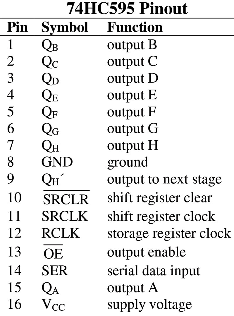
Figure 1.
Let’s look at the key features. A single bit (either a zero or a one) is placed on pin 14 — the serial data input. When a low-to-high transition is applied to pin 11, that bit is clocked in to the first stage of the shift register, but only after all other bits are bumped ahead one notch to make room for it. The current contents of the shift register are still “invisible.” If, however, a clock signal is next applied to pin 12, then the presently concealed contents are latched into an external storage register and appear on the associated output pins.
So, the steps are: (a) put a bit on the serial input; (b) strobe the shift register clock; and (c) strobe the storage register clock to make the bits appear on the outputs. By carrying these steps out eight times in a row, an entire byte coming in serially is moved bit-by-bit down the conveyor belt and finally appears on the output pins, QA through QH. If, for some reason, you’d like to clear everything out and start with all zeros again, a high-to-low pulse on pin 10 will accomplish that.
We won’t need most of the other pins (except for power, obviously) and will worry about the details when we get to the schematic.
Figure 2 shows the pinout for a typical LCD.
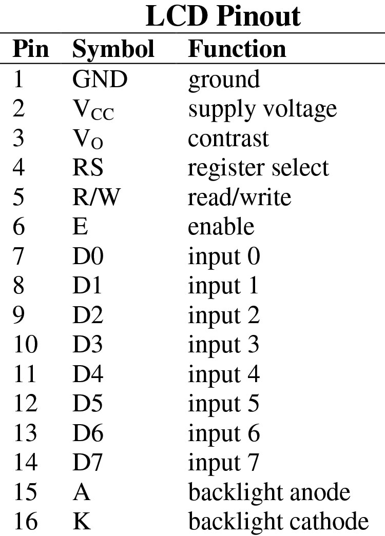
Figure 2.
Most of these are set to operate either as eight-bit or four-bit parallel devices, but the latter is more than fast enough for any application I’ve ever come up against. So, we’ll jettison pins 7 through 10 at once simply by grounding them. Anytime we need to send a byte to the device, we’ll do so in halves, transmitting one nibble (four bits) at a time.
LCDs do have the ability to talk back, but that feature is almost never required. So, we’ll also ground pin 5 which is the Read/Write line. This is a one-way street.
It's possible to send either a command or a character to the LCD. Commands take care of such things as clearing the screen, homing the cursor, and so forth. Characters are indicated by means of the ubiquitous ASCII code set.
To let the display know what the incoming byte (or more accurately, pair of nibbles) represents, use pin 4 — the Register Select (RS) line. When this is low, the byte stands for a command; when high, it is a character.
Once either a command or character has been placed on the data lines, a quick low-to-high pulse on the Enable line (E) at pin 6 locks it in. A pulse width of a couple microseconds will do the trick.
The few remaining lines are fairly pedestrian in nature and will be explained once we get to the complete circuit. At this point, you have a basic understanding of the pins of both the 74HC595 and the LCD at your fingertips.
As you’ll see, it’s remarkably easy to mate the two parts. So, let’s cut at once to the gestalt!
How They Go Together
Figure 3 shows the schematic for a complete working circuit, consisting more of wires than anything.
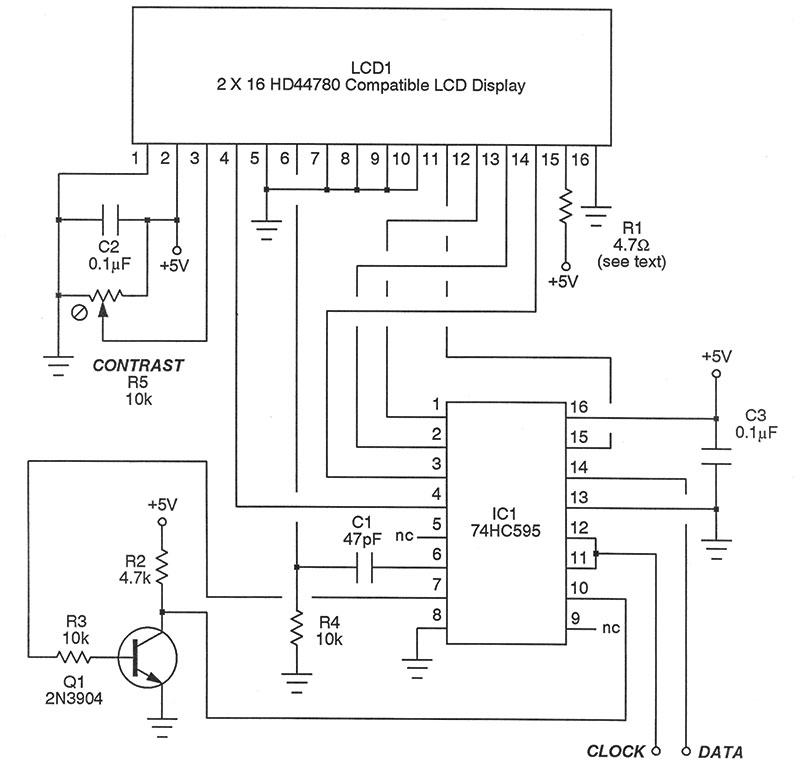
Figure 3.
Let’s chase them down. Outputs QA through QD of the 74HC595 connect to data inputs D4 through D7 of the LCD, respectively. Recall that inputs D0 through D3 are grounded and not needed for four-bit operation. Output QE of the chip drives the Register Select input of the LCD. Output QG feeds the Enable input of the LCD, but only after being processed by C1 and R4.
You can think of this RC network as being a differentiator if you want, or else as a half-monostable if that term is more comfortable. The purpose is simply to make sure the eventual Enable strobe is shorter than the actual signal appearing on QG.
IC1 output QH is first inverted by transistor Q1 and then fed back to IC1 to provide a reset or clear operation. The inversion is necessary since the shift register clear pin expects negative logic. If you already have an uncommitted inverter kicking around in your design, you can use it instead and then eliminate Q1, R2, and R3.
Output QF is not needed and is simply left unconnected. Output QH’ (note the prime symbol there) is also left floating. This pin is normally employed when ganging several of the chips for more bit outputs.
The shift register clock and storage register clock lines (pins 11 and 12) are tied together and simply become the clock input. When configured in this manner, the storage register (the latch outputs, in other words) will always be one step behind what’s happening internally within the shift register.
The serial data input is found at pin 14 of IC1. Pin 8 is ground, while pin 16 is +5V. Pin 13 is also grounded to enable the tri-state outputs of the 74HC595.
Back to the LCD. Pin 3 is used to set the contrast of the display; connect it to a potentiometer or trimmer.
Pins 15 and 16 take care of the backlight LED, if any. Some units require a resistor as shown in the schematic (R1), while others need a power rectifier. Use whatever the datasheet for your particular LCD specifies.
Lastly, pin 1 is the LCD ground, while pin 2 is +5V. For reliable operation, it’s very important to straddle these with a 0.1 µF disc capacitor.
The Grand Dance
With the hardware out of the way, it’s now time to choreograph the flow of bits. Obviously, this will be handled by the microcontroller you choose to use. Let’s not worry about the actual code here, but instead focus on what has to happen and when. Figure 4 shows the road map.
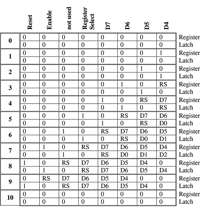
Figure 4.
Now, don’t panic because the progression displayed there is very linear in nature, as you’d expect in serial-to-parallel conversion. The steps are labeled 0 through 10. Furthermore, each row is split in two, showing what the shift register currently holds and what the storage register (called the latch from now on) is presently outputting to the LCD. Don’t forget that the latch is always one clock pulse behind the shift register. Let’s see what happens.
At the outset (Step 0), both the register and the latch are clear; this is the normal condition during quiescence. In Step 1, a one is input. This will eventually first become the enable pulse in Step 8, and then the reset pulse in Step 9.
In Step 2, a zero is fed in. Its purpose is to bring the Enable pulse low again in Step 9.
Step 3 pumps in the RS bit — either zero for a command or one for a character. By the time we get to Step 8, it will obviously be controlling the RS line going to the LCD.
Steps 4 through 7 shift in the four data bits comprising a nibble — a pair of which will eventually make up an entire command or character byte. Keep pulsing the clock away and in time, the bits will arrive at their desired positions.
Now, Step 8 is where the action really occurs. Data lines D0 through D4 are in place, as are the RS and Enable bits. The data is locked in to the LCD here. Then in Step 9, the Enable line goes low once more, followed by a reset a split second after that. The 74HC595 is forced to an all-clear state in Step 10, which is back where we originally started.
Thanks to the software download for this article, you don’t really have to know all of the ins and outs. Nonetheless, it really is instructive to work through the steps with a pencil in your hand, just so you learn how a shift register works.
The Software
Just to show what’s all possible with this rig, I put together a complete software package consisting of a demonstration program along with the necessary drivers. This has been implemented for the popular PIC12F683 microcontroller which is, in fact, an eight-pin device just begging for a two-line LCD.
It’s simple enough to change it over to any other PIC or, for that matter, port the entire software to just about any other controller you have in mind. Look to the sidebar to learn how to get the source code.
About the Software
Like many modern electronics projects, this one depends a fair amount on software components as well. Fortunately, all of the programs required here are absolutely free of charge. Let’s start with the firmware for the PIC microcontroller.
In the downloads, you'll find source code for the drivers and a complete program demonstrating just about everything an LCD can do. The code is written in the excellent Great Cow Basic language. The nice thing here is that this language supports parameter passing and program structures like procedures and functions, so all the routines are just lying there ready for you to pluck for your own work.
If you feel the need, you can even port the code over to an existing commercial Basic language like PICBasic PRO, since the syntax is virtually the same. In any event, the drivers contain routines for sending nibbles, and complete commands and characters, along with a set of equates for unlocking all of the other features in an LCD.
You can download an absolutely free copy of the Great Cow Basic compiler here. There are no restrictions and no hidden catches.
The download package for this article also contains everything you need if you’d like to build the piggy-back module I described. In particular, you’ll find .pdf files of the printed circuit board (PCB) artwork and a parts placement guide, along with the complete original file. This has been created with FreePCB — an exceptionally fine PCB design package. As the name suggests, it too is completely gratis. You’ll find it at www.freepcb.com.
The PCB was designed as a double-sided affair which could certainly be sent to a professional etching facility. Since the only top-side traces are straight lines, I actually etched my own single-sided board and simply installed jumper wires on top. It was quick and easy, and works very well.
Figure 5 shows the circuitry for the PIC12F683 and how to connect it to the two-line LCD.
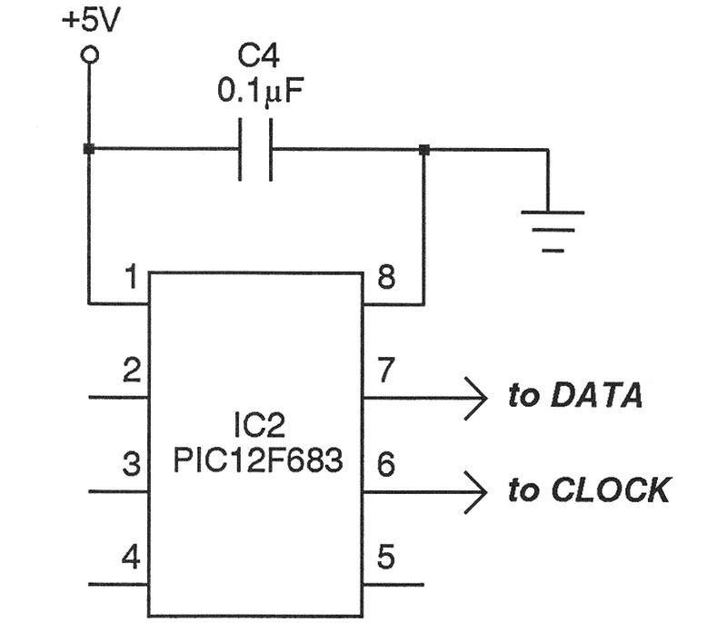
Figure 5.
Not much to it, is there? So, give it a try. Compile and assemble the code, and then Flash it to the microprocessor. Upon power-up, you will be treated to a demonstration of all sorts of things that are possible such as blinking, scrolling, panning, extended character sets, and more.
A Stand-Alone Package
One final thing before I turn you loose to come up with your own application. I thought it might be handy to have an all-in-one arrangement for the two-wire LCD. To this end, the download package for this article also includes the printed circuit board artwork to make a piggyback affair for most any LCD you bump into.
It’s been designed to permit easy connection to a solderless breadboard during testing stages of circuits incorporating the two-wire LCD.
Figure 6 shows both a typical LCD, along with the piggyback board implementing this circuit.
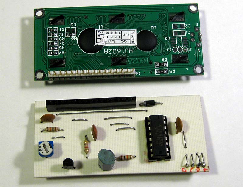
Figure 6.
Figure 7 shows what it looks like when the two are snapped together.
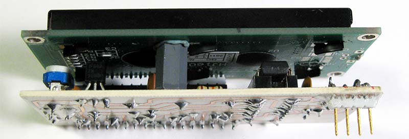
Figure 7.
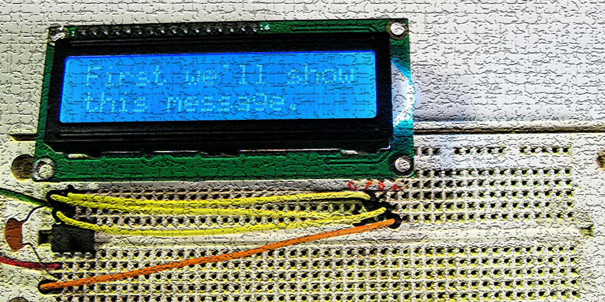
Figure 8 shows the entire rig on a breadboard, shining away.
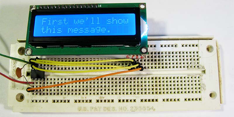
Figure 8.
So, let’s hear no more of that all-too-common groan, “I’ve run out of port lines!” NV
Parts List
| Passive Components |
|
| R1 |
4.7W (see below) |
| R2 |
4.7K |
| R3,R4 |
10K resistor |
| R5 |
10K trimmer |
| C1 |
47 pF disc capacitor |
| C2,C3 |
0.1 mF disc capacitor |
| Semiconductors |
|
| Q1 |
2N3904 NPN transistor |
| LCD1 |
2x16 LCD display |
| IC1 |
74HC595 shift register |
Note: The backlight in an LCD typically requires something to drop the voltage a bit. In the unit shown here, R1 was specified. Sometimes, however, a rectifier is used. Check the datasheet for whatever LCD you employ.