Microcontrollers are very popular with electronics hobbyists, and why not? You write software that tells the hardware what to do — complete with a wide range of peripheral features and capabilities. It is not unlike programming your home computer. Hackers have done amazing things with them, pushing the performance envelope beyond what they were designed to do. However, what is even better than writing software for hardware? How about writing hardware? How about telling the hardware what to be versus what to do? Enter the exciting world of Field Programmable Gate Arrays (FPGAs)!
Introduction
We live in a renaissance for the electronics hobbyist with new and exciting products, kits, development boards, and software hitting the ”streets” daily (okay, online stores). Whether it is the Arduino, the Raspberry Pi, RTL-SDR, or the multitude of other products, there is literally something for everyone. Lately, this includes various affordable FPGA development boards. In the past, FPGAs were traditionally the domain of electrical engineering companies with significant resources and capital, but now these boards are opening up a new and exciting world to the hobbyist.
There are several options for those curious about FPGAs. The two largest FPGA companies and industry leaders — Xilinx and Altera — have development kits available for their various product families from $180 and up. Digilent — probably most famous with hobbyists for their chipKIT PIC32 Arduino boards — has several options for as low as $90. These development boards usually include additional hardware such as switches, LEDs, and VGA connectors to aid in your experimenting.
However, recently there have been several offerings from independent developers, such as the Papilio (as low as $40) and the Mojo ($75). These boards have limited additional hardware; however, they are typically open source and are easily extensible. This article will focus on the latter — the Mojo V3 from Embedded Micro.
In this article, I will not cover the details of how a FPGA works in regards to LUTs, slices, etc. Nor will I cover an introduction to Verilog. Instead, this article will get you up and running with FPGAs — no prior experience required. Once you are comfortable with the basics of setting up the software and loading and running a circuit on the FPGA, I recommend you reference the Nuts & Volts article, “Up The Logic Food Chain” (August 2008) for a more detailed discussion on the ins and outs of FPGAs.
You Gotta Have Mojo, Baby
The Mojo V3 board is built around the Xilinx XC6SLX9 which is part of the low cost Spartan-6 family. Sporting over 9,000 logic cells, 16 DSP slices, and 102 I/O pins (84 available for use on the Mojo V3), there is plenty of room to learn! An integral part of the board design is an Atmel AVR ATmega32U4 used to configure the FPGA, USB communications, and to assist with analog-to-digital conversion (ADC). Additionally, there are eight LEDs and a pushbutton on the board available to the user.
The Mojo V3 arose from a Kickstarter project and boasts both open source software and hardware. Be aware, you have to supply a micro USB cable and an optional 5-12 VDC power supply if you need to draw more current than your USB port can safely provide (typically 500 mA).
Where Do I Begin?
There is a significant software stack in order to begin using the Mojo V3. However, all of it is free of charge. The first order of business is to download ISE Design Suite 14.7 from Xilinx (if you cannot download the full DVD ISO, Xilinx will mail you a DVD free of charge). Unfortunately, the software is only for Windows and Linux, as the world of FPGAs is not yet Mac friendly. As a Mac user myself, I got around this by running Linux Mint 17.1 in Parallels Desktop 10 and it works flawlessly.
If you don’t want to shell out the money for Parallels Desktop, you should have no problem running Linux Mint in VirtualBox. (I have been using VirtualBox for a Windows XP virtual machine for years.) Installation is fairly easy, but be aware that it does take a significant amount of space (20+ GB). For a detailed installation tutorial, please see Embedded Micro’s Installing ISE Tutorial.
The next piece of software you’ll need is the Mojo Loader. This software is produced by Embedded Micro and — once again — is only for Windows and Linux. As with ISE Design Suite, Embedded Micro has an excellent installation tutorial.
Optional software includes the Arduino IDE (integrated development environment) and the Mojo IDE. If you are savvy, you can load the onboard ATmega32U4 with custom software to utilize the full potential of the microcontroller for whatever you desire. I have not tried the Mojo IDE which is designed for development outside of the ISE Design Suite (although it is still required for the command line tools), as it is still very much in beta.
Project Setup Basics
Okay, with our software stack installed, let’s design something! I think an easy starting point is a 2-to-4 line single bit decoder with Enable. This project will allow us to investigate some basic combinational logic using the Mojo V3. However, before we can start writing hardware (sounds weird, doesn’t it?), let’s cover the basic steps to create a project in ISE Design Suite.
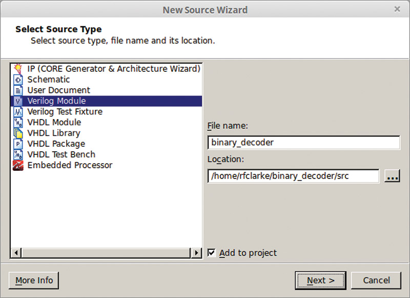
With the software open, create a new project (File->New Project...). Name the project binary_decoder and add /syn to the end of the Working Directory (trust me on this... ISE loves to make files and this will contain the mess). Click Next (Screenshot 1).
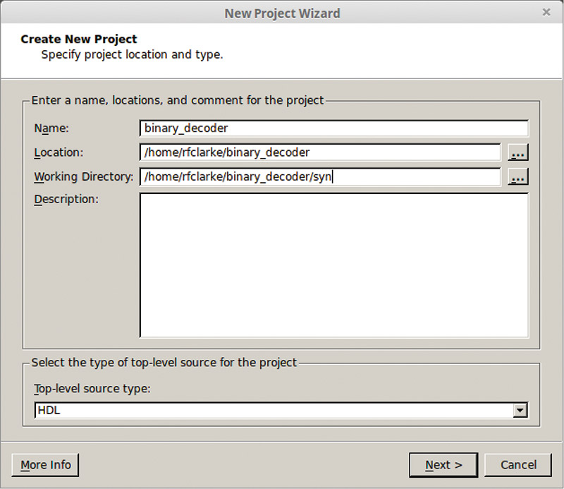
SCREENSHOT 1. Create New Project.
We need to specify some project settings. The Family should be set to “Spartan6” and the Device to “XC6SLX9.” The Package is “TQG144” and the Speed is “-2.” Now, you’re probably asking me, “How do you know the speed is -2?” Great question!
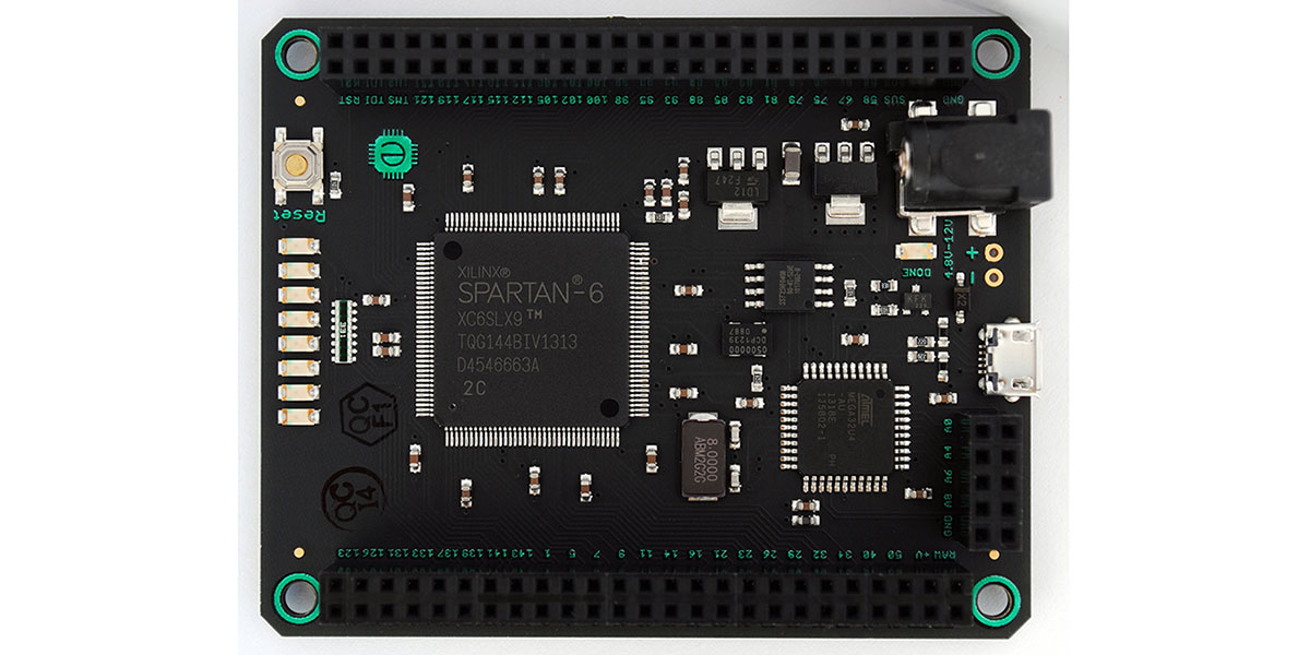
If you look at the FPGA package on the Mojo V3 board, the last line of text says “2C” (Photo 1).
PHOTO 1. Mojo V3.
Reading the Spartan-6 Family Overview Datasheet, this indicates a speed grade of “-2” and a commercial temperature tolerance.
Lastly, verify that “Verilog” is selected as the Preferred Language. Click Next (Screenshot 2).
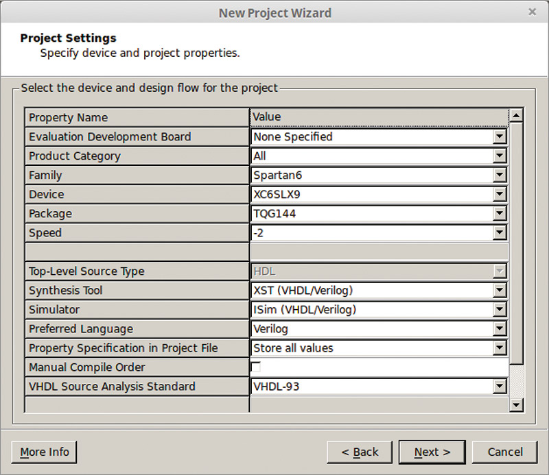
SCREENSHOT 2. Project Settings.
Click Finish on the next window, titled Project Summary.
As stated, we’ll be designing a 2-to-4 line single bit decoder with Enable. Let’s create the Verilog source for the decoder. Create a new source (Project->New Source), select Verilog Module, and name the file binary_decoder. Add /src to the end of the Location and click Next (Screenshot 3).
SCREENSHOT 3. New source file.
At the next window — titled Define Module — just go ahead and click Next; we’ll define our I/O ports later. In the Summary window, click Finish. When it asks to create the src directory, click Yes.
Okay, okay. I know you’re chomping at the bit to start coding, but there is only one more step I promise! Select binary_decoder in the Implementation Hierarchy, look below at the Processes tree, and right-click on Generate Programming File. Select Process Properties, check Create Binary Configuration File, and click OK. Done! Let’s write some hardware!
Technologic
Okay, don’t get mad, but ... I may have lied to you back there. Before we can start coding, we need to first look at the truth table for a 2-to-4 line single bit decoder (Figure 1).
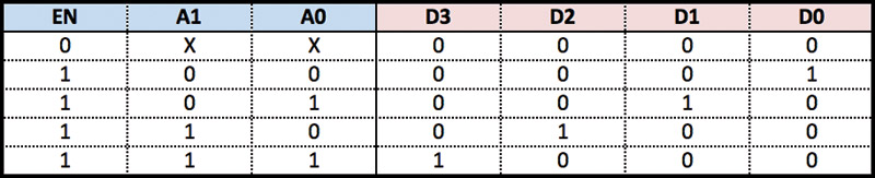
FIGURE 1. A 2-to-4 line binary decoder with Enable truth table.
It’s pretty simple, really. The two-bit binary input, A, corresponds to a specific bit in D, which is four bits wide. For example, an input of A = 10 and EN = 1 creates an output of D = 0100. In other words, A = 2 corresponds to D2 = 1. The logic gate diagram for the truth table is shown in Figure 2.
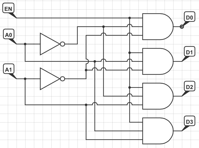
FIGURE 2. The 2-to-4 line binary decoder with Enable circuit diagram.
This is pretty easy to write in Verilog, so let’s do it! Copy the following Verilog code into the source file we just created — binary_decoder.v:
// gate-level 2-to-4 line decoder
// with enable
module binary_decoder
(
input wire en,
input wire [1:0] a,
output wire [3:0] d
);
assign d[0] = en & ~a[0] & ~a[1];
assign d[1] = en & a[0] & ~a[1];
assign d[2] = en & ~a[0] & a[1];
assign d[3] = en & a[0] & a[1];
endmodule
While this is not a tutorial on Verilog itself, let’s break down our code real quick. The first portion of the module defines the inputs and output. We have a single bit input labeled en and a two-bit input labeled a. The four-bit output is labeled d. The last portion simply defines the output as the set of four three-input AND gates, with the appropriate inputs inverted per the truth table. Easy!
Okay, let’s actually define our I/O pins. Create a new source, but instead of a Verilog Module, define it as an Implementation Constraints File. Name it binary_decoder and copy the following code into the source file:
CONFIG VCCAUX = 3.3;
NET “en” LOC = P139 | IOSTANDARD = LVCMOS33;
NET “a[0]” LOC = P137 | IOSTANDARD =
LVCMOS33;
NET “a[1]” LOC = P138 | IOSTANDARD =
LVCMOS33;
// Mojo V3 LED 2-5
NET “d[0]” LOC = P134 | IOSTANDARD =
LVCMOS33;
NET “d[1]” LOC = P133 | IOSTANDARD =
LVCMOS33;
NET “d[2]” LOC = P132 | IOSTANDARD =
LVCMOS33;
NET “d[3]” LOC = P131 | IOSTANDARD =
LVCMOS33;
This file defines which pins are associated with the I/O ports in our modules. The first line is related to how the Mojo V3 is designed. The VCCAUX pins of each of the I/O banks are tied to 3.3V. Long story short, this means we are restricted to 3.3V logic. The other lines should be fairly self-explanatory.
That’s it! How about we go for a test drive?
Simulation
Before we generate the programming file, let’s take a look at ISim in order to verify that our Verilog code works. To do this, we need to create a Test Bench. Create a new source file, define it as a Verilog Test Fixture, and name it binary_decoder_test. Copy the following source code into the newly created file:
`timescale 1 ns / 10 ps
module binary_decoder_test;
// test inputs and outputs
reg en;
reg [1:0] a;
wire [3:0] d;
// unit under test
binary_decoder uut(.en(en), .a(a),
.d(d));
// run tests for all iterations of
// en and a, 250 ns per test
initial begin
en = 1’b0;
a = 2’b00;
# 250;
en = 1’b0;
a = 2’b01;
# 250;
en = 1’b0;
a = 2’b10;
# 250;
en = 1’b0;
a = 2’b11;
# 250;
en = 1’b1;
a = 2’b00;
# 250;
en = 1’b1;
a = 2’b01;
# 250;
en = 1’b1;
a = 2’b10;
# 250;
en = 1’b1;
a = 2’b11;
# 250;
$stop;
end
endmodule
The quick and dirty version of what this does is as follows: We define a set of registers and a wire that correspond to the inputs and output of our device. The Test Bench is then written to test each input iteration of en and a at a 250 ns interval.
I’m sure your next question is, “How do we see the results?” Another great question! With Simulation view selected in ISE Design Suite, select binary_decoder_test in the Behavioral Hierarchy and double-click on Simulate Behavioral Model in the Processes tree below. The ISim software should open automatically.
Select the Simulation->Run All menu option and then reselect the Default.wcfg window. Select the View->Zoom->To Full View menu item and you should now be able to view the results of the Test Bench (Screenshot 4).
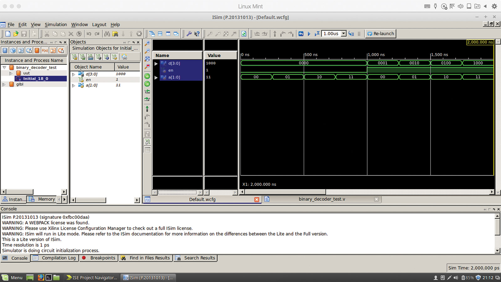
SCREENSHOT 4. ISim simulation output.
As you can see, our implementation of the 2-to-4 line decoder with Enable works as advertised.
Synthesis
Okay, time for the fun part. Let’s load the Mojo V3 and test the hardware! Close ISim and go back to the Implementation view. Select binary_decoder and in the Processes tree, double-click on Generate Programming File. It takes a surprising amount of time to generate the binary file for the FPGA, so be patient. Once it is complete, you should find the binary_decoder.bit file in the syn sub-directory of your root project directory. Following Embedded Micro’s Creating a Project tutorial, connect your Mojo V3 and program the FPGA.
To test the circuit, I wired up an eight-pin DIP switch with 10K pull-down resistors to easily toggle the inputs. Position “1” corresponds to A0 and position “2” corresponds to A1. As you can see in Photo 2, with an input of A = 11, the output is D = 1000 as expected!
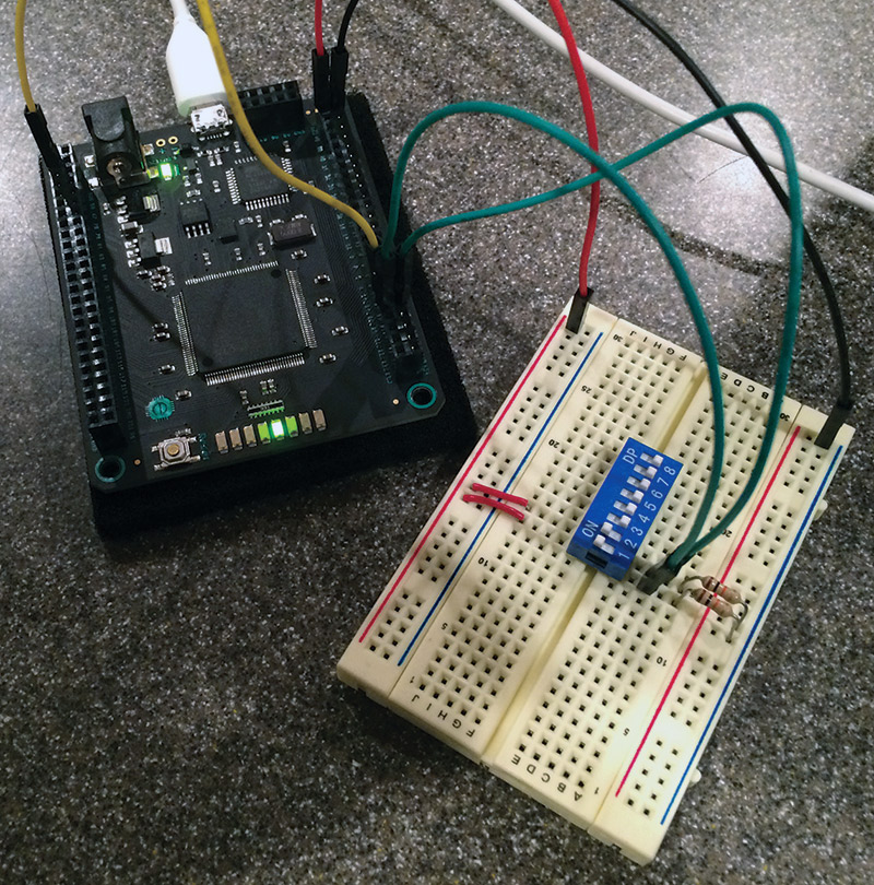
PHOTO 2. Circuit test: EN = 1; A = 11; and D = 1000.
Photo 3 is the same value of A with EN tied to ground, therefore disabling the output.
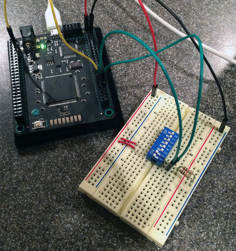
PHOTO 3. Circuit test: EN = 0; A = 11; and D = 0000.
Now What?
To learn more, I recommend the book FPGA Prototyping By Verilog Examples by Dr. Pong P. Chu. This is the book I am currently working through myself, and it is very easy to follow. In fact, the example circuit we wrote in this article is one of the first suggested exercise experiments by the author.
While the book is written for an older Digilent Spartan-3A development board, it is fairly easy to port them over to the Mojo V3 or any other FPGA board you might be using. You may have to supply some extra hardware, but you probably have most of it lying around your junk box. Of note, if VHDL is your thing, Dr. Chu has an identical book written for that particular language.
So, you may be asking yourself, “What else can I do besides combinational logic?” The answer is ... virtually anything in the digital world! Want to generate VGA or NTSC signals? No problem (with the help of some digital-to-analog conversion, of course). How about a custom microcontroller core? Yup. An entire recreation of the Nintendo Entertainment System? It’s been done! An IBM PC or Apple II? Absolutely!
The learning curve is steep — especially if you are accustomed to procedural programming and microcontrollers. However, once you wrap your mind around how the FPGA operates, its parallel structure, and have an understanding of digital logic, the possibilities are truly endless! NV
RESOURCES
Embedded Micro
https://embeddedmicro.com
Xilinx ISE Design Suite 14.7
www.xilinx.com/support/download/index.html/content/xilinx/en/downloadNav/design-tools.html
Parallels Desktop
www.parallels.com/products/desktop
Papilio
http://papilio.cc
Digilent FPGA Boards
www.digilentinc.com/Products/Catalog.cfm?NavPath=2,400&Cat=10&FPGA
FPGA NES
http://danstrother.com/fpga-nes
FPGA Apple II+
www.cs.columbia.edu/~sedwards/apple2fpga
Downloads
What’s in the zip?
Code files
binary_decoder_text.v
binary_decoder.v
binary_decorder.ucf