This article describes a piece of lab test equipment that combines a variable DC voltage reference, a programmable function wave generator, and a fully functional frequency counter.
This project started as a microcontroller controlled variable voltage reference (VVR) using just a PIC, a fixed voltage reference, and a digital-to-analog converter (DAC). The project then expanded to include a programmable function generator (PFG) that can produce a sine wave, triangle wave, square wave, etc. I also needed a mechanism to measure the frequency of the function generator output, so I added a frequency counter capability to the PIC. The total parts cost of this multifunction tester are well under $200 (includes components, power supply, cabinet, all front panel parts, printed circuit boards [PCBs], etc.).
The key component of the design is the eight-bit DAC0800 digital-to-analog converter shown in Figure 1.
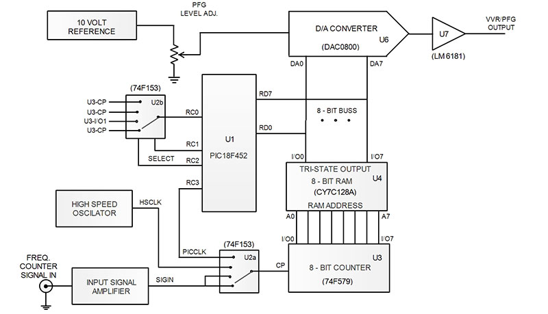
FIGURE 1. The 3-in-1 tester block diagram.
The analog output of the DAC0800 is connected to the LM6181 op-amp. The DAC0800 digital input can be connected either to the eight-bit PIC port D or to the input/output (tri-state) buss of an eight-bit RAM. As I describe the design of the tester, the interaction between the components will become clearer.
At the top left of Figure 1 is a 10 volt (I actually use two five volt diodes in series) voltage reference that determines the DAC maximum output voltage. When in the function generator mode, a front panel level adjust potentiometer sets the actual peak-to-peak output voltage.
When in the VVR mode, the potentiometer is bypassed and the PIC sets the output level. The LM6181 is a high performance amplifier that can output ±10 volts at ±100 milliamps.
In the VVR mode, the LM6181 input connection is set for unipolar output by grounding the plus input of the LM6181; the PIC port D is set as an output; and the RAM tri-state output is turned off so the PIC has complete control of the DAC0800 output.
If port D is set to binary 00000000, the LM6181 output will be zero volts; if port D is set to 11111111, the LM6181 output will be +10 volts. Since there are 256 possible binary numbers between 00000000 and 11111111, there are also 256 possible output voltages.
The PFG mode can be implemented this way by having the PIC repeatedly output the values describing the function (for example, the sine wave amplitude values), but the maximum frequency attainable will be limited because the PIC — in addition to outputting function values — must also continuously read the front panel switches and perform the frequency counter work.
In my design, I decided to offload the PFG DAC updates to external circuitry: the eight-bit RAM (U4), the eight-bit counter (U3), and the high speed oscillator. This PIC is no longer in the repetitive PFG loop and it can perform the housekeeping duties mentioned above.
We finally get to the frequency counter. Here, I implement a technique I used in an earlier Nuts & Volts article on frequency counters. The common hobbyist frequency counter design sets up a fixed gate interval (say, one second) and then counts the number of input cycles during that interval. With a one second gate, the number of input cycles is equal to the input frequency with a ±1 cycle resolution.
This works very well if the input frequency is high because the ±1 count error can be ignored. However, at low frequencies, the ±1 count error can be very significant.
To accurately measure a low input frequency, the gate interval must be increased, or the counter can measure the period of the input signal. In my design, I automatically switch to a period measurement when the input frequency is less than 150,000 Hz. This is discussed in detail below.
Variable Voltage Reference
In the VVR mode (see Figure 2), the PIC sets the VVRMode bit which — with relay K1 — configures the DAC0800/LM6181 pair for zero volts output when the PIC outputs binary 00000000 on port D, and +10 volts for binary 11111111.
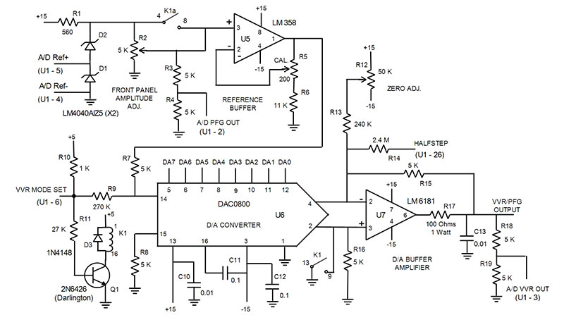
FIGURE 2. Digital-to-analog converter schematic.
If we use 00000000 as a starting point, there are then 255 voltage steps to get to +10 volts. Therefore, each step is 10/255 or 0.0392 volts. This is an awkward value since it leads to non-integer values. For example, if we want a 5.2 volt output, we need a buss digital value of 5.2/0.0392 or 132.6.
Rounded to 133 it produces 133 x 0.0392 or 5.216 volts — a .3% error.
I get rid of this error by simply using 250 as the number of steps to 10 volts, so the voltage per step is 10/250 or exactly 0.040 volts. Now, the 5.2 volt setting is 5.2/0.040 or 130, exactly 5.2 volts. This works for all voltages that have an even number for the fractional part (5.0, 5.2, 5.4, etc.).
With an odd fractional part like 5.3 volts, the setting is 5.3/0.0400 or 132.5, and all voltages with an odd fractional value will have a half bit remainder. I correct this error by using a HALFSTEP control line on the PIC which effectively adds a ninth bit to the DAC0800. This is shown at the right in Figure 2.
If HALFSTEP is set high, the 2.4 megohm resistor decreases the output of the LM6181 by 0.020 volts or one half bit. So, to get 5.3 volts, we set the PIC output to the next integer value of 133 (5.32 volts) and set HALFSTEP which reduces the voltage by 0.020 volts; we then get 5.32 – 0.020 = 5.30 volts. This works for all voltages with an odd fractional part.
The upper left of Figure 2 shows the input reference diodes and buffer amplifier. I use the PIC built-in analog-to-digital converter (ADC) to measure various voltage points in the tester. This ADC requires a fixed voltage reference of no more than 5.5 volts, but the VVR mode requires a 10 volt reference.
The five volts for the ADC reference can be divided down from a 10 volt reference diode with two precision resistors or — for best accuracy — I use two five volt reference diodes in series (as shown in Figure 2) and pick up the ADC reference voltage from the bottom diode D1. In fact, the upper diode D2 doesn’t need to be as accurate as D1 since the calibration potentiometer (R5) will be used to correct any error.
Front panel potentiometer (R2) sets the peak-to-peak output in the PFG mode. Resistors R3 and R4 divide this voltage in half for the PIC ADC, which reads and displays the peak-to-peak voltage in the PFG mode. Potentiometer R5 is internally mounted and is used in the calibration of the tester.
The VVR mode is selected when the PIC sets the VVRMode bit. Two things happen: First, the double pole relay K1 is energized and contact K1a bypasses potentiometer R2, connecting the full 10 volts to amplifier U5; and contact K1b grounds the plus input of the LM 6181 (U7) setting unipolar operation. Second, R9 raises the 10 volts applied to the DAC0800 by about 2% so that 250 steps yields 10 volts in the VVR mode and 255 steps yields 10 volts in the PFG mode.
Front panel switches SW2 and SW3 set the VVR voltage. SW2 is a single pole 11-position switch that selects the integer voltage: 0, 1, 2 ... 10 volts. SW3 is a single pole 10-position switch that selects the fractional voltage: 0, .1, .2, .3 ... .9 volts.
Calibration of the VVR/PFG does not require any external equipment because of the accuracy of the PIC ADC coupled with the accurate five volt reference diode D1. Just follow these steps:
- Set the VVRMode bit and clear the HALFSTEP bit.
- Set SW2 to zero volts and SW3 to .2 volts.
- Adjust the ZERO ADJ, internal potentiometer R12, until the display reads 0.2 volts.
- Set SW2 to 10 volts and SW3 to zero volts.
- Adjust the AMPLITUDE ADJ, internal potentiometer R5, until the display reads 10 volts.
- Repeat steps 2 through 6 a few times.
Programmable Function Generator
I’m going to use a sine wave function to demonstrate the operation of the PFG. If you look at a sine wave, you will see that a complete cycle consists of four distinct quadrants that have a similar shape.
For example, if we want our sine wave to have the full eight-bit capacity of the DAC (128 plus and 128 minus amplitude steps) for a complete sine wave cycle, then we must also have 256 time steps (one for each amplitude step).
The 256 amplitude steps for each complete sine wave cycle correspond to 64 amplitude steps for each of the four quadrants of the sine wave. So, in order to generate a 20 kHz sine wave at 64 step resolution, the PIC must send 256 x 20,000 or 5,120,000 update steps to the DAC per second.
The PIC18F452 that I chose for this project has a PLL that multiplies the input (10 MHz) by four to 40 MHz, but the instruction rate is one quarter of that or 10 MHz. This means the updates can’t take more than four instruction cycles each. At the same time, the PIC has to monitor all of the front panel switch settings (using the built-in ADC), drive the display, and handle the frequency counter function (discussed below).
Using the interrupt control to do the updates just makes matters worse because of the time spent processing interrupts.
As I mentioned in the opening remarks, I decided to offload the DAC updates to external circuitry (see Figure 3): the eight-bit RAM (U4), the eight-bit counter (U3), and the high speed oscillator.
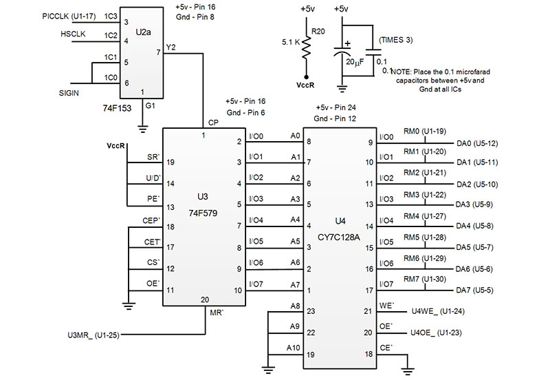
FIGURE 3. RAM and RAM addressing schematic.
When you select a function (for example, a sine wave), the PIC loads the RAM with the 256 amplitude constants that define one complete cycle of the sine wave. The PIC then disconnects from the RAM and goes about performing the other tasks.
The high speed oscillator is connected to the eight-bit counter via the multiplexer U2a and the RAM continuously cycles through the DAC steps; out comes a sine wave. The user can program any function: square wave, triangle wave, pulse, etc,. to go into the RAM.
Sixty-four steps per quadrant is very high resolution and is probably more than required. ON-OFF-ON toggle switch SW4 sets the resolution at 16, 32, or 64 steps per quadrant. For 32 steps, the RAM is loaded with two complete cycles of the function using every other amplitude step from the 64-bit step list. This also doubles the output frequency. For 16 steps per quadrant, four complete cycles in the RAM are used.
Loading the RAM data is a little bit tricky because the PIC has no direct connection to the RAM address buss (A0 through A7 on U4). So, I have to go through the eight-bit counter U3 to get to the RAM address buss.
U2a sets the clock input on U3 to PICCLK — an output pin on the PIC that is toggled high/low to simulate a clock pulse. The PIC then sets port D as an output, pulses the Master Clear pin on U3 setting the RAM address at 00000000, and then places the RAM data on the buss.
The PIC then toggles the Write Enable on the RAM to store the location 00000000 function data. The PIC then toggles PICCKC to advance U3 to RAM location 00000001, and repeats the storing sequence until all RAM locations are filled.
Frequency Counter
The frequency counter generally follows the traditional model where a fixed gate interval (say, one second) is set using a PIC counter (TIMER2) running off the 10 MHz clock. A second PIC counter (TIMER1 – RC0 input) counts the number of input cycles during that interval.
With a one second gate, the number of input cycles is equal to the input frequency (with a ±1 count error).
This works very well if the input frequency is high because the ±1 count error can be ignored. However, to accurately measure a low input frequency, the gate interval must either be increased, or the counter can be set to measure the period of the input signal.
With the latter technique, the roles of TIMER1 and TIMER2 are sort of reversed. TIMER1 still sets the gate interval and still counts the input cycles, but it’s programmed to count a specific whole number of input cycles so there is no ±1 error here.
Meanwhile, TIMER2 counts the 10 MHz system clock during this gate interval; it has the ±1 count error but the error is one in 10 million (the system 10 MHz clock).
For example, if the input signal is 1 MHz, then using the traditional frequency counter model and a one second gate interval, the error will be ±1 input count in one million — not bad. If the input signal is 100 Hz, the ±1 count is one in 100 — not very good. If we instead set the gate interval to be exactly 100 input cycles (one second), TIMER2 will read 10 million ±1 count — excellent.
In my design, I automatically switch to a period measurement when the input frequency is less than 150,000 Hz. I do this by making a preliminary measurement of the input frequency using a 0.1 second gate interval. If the frequency is greater than 150,000 Hz, I do a one second final frequency measurement.
Otherwise, I switch to a period measurement. With this technique, I get frequency measurements accurate to five/six digits every 1.1 seconds over the entire frequency range of 10 Hz to over 10 MHz.
I want the period measurement to last for about one second. From the .1 second frequency trial measurement, we get an approximate value for the input frequency — say, 99 Hz. This means the input frequency is between 98 and 100 Hz (the ±1 count error).
Assume the input frequency is exactly 99.56 Hz. I set TIMER1 to 99 (for the approximately one second gate time) and get the total number of 10 MHz clock pulses in 99 pulses of the input signal.
Since the input frequency is actually 99.56 Hz and it has a period of .0100442 seconds, the total gate time will be 99 x .0100442 or .994376 seconds.
Meanwhile, TIMER2 is counting the 10 MHz clock (having a period of .0000001 seconds) and will end up with .994376/.0000001 or 9,943,760 clock pulses for 99 input cycles. So, the actual period of the input signal is (9,943,760 x .0000001)/99 or .01004442 seconds, or 99.56 Hz — perfect!
There are many designs for a frequency counter input amplifier available on the Internet (also check out the design I used in the above referenced article). For this project, I simply use an available inverter (U8f) which is used for the high speed oscillator. To prevent any interference, I turn the oscillator off in the frequency counter mode.
U2 is a 74F153 dual 4-to-1 multiplexer that is controlled by the PIC via the Select (SA, SB) lines as follows:
00. Used in normal frequency counter mode (SIGIN from input amplifier).
01. Used in frequency counter mode (SIGIN from input amplifier divided by four).
10. Used in PFG mode with clock from high speed oscillator (HSCLK).
11. Used in PFG mode with clock directly from the PIC (PICCLC).
U2a sets the clock input to the eight-bit counter (U3) to one of the following inputs:
00. Frequency counter input (SIGIN from input amplifier).
01. Frequency counter input (SIGIN from input amplifier).
10. High speed clock (HSCLK).
11. Clock from PIC (PICCLK).
U2b sets the input to the frequency input pin on the PIC (RC0) to one of the following inputs:
00. The clock pin on the eight-bit counter (U3-CP).
01. The second stage output on the eight-bit counter (U3 – I/O1).
10. The clock pin on the eight-bit counter (U3-CP).
11. The clock pin on the eight-bit counter (U3-CP).
PIC18F452 Microcontroller
I chose the PIC18F452 (see Figure 4) for this project for several reasons.
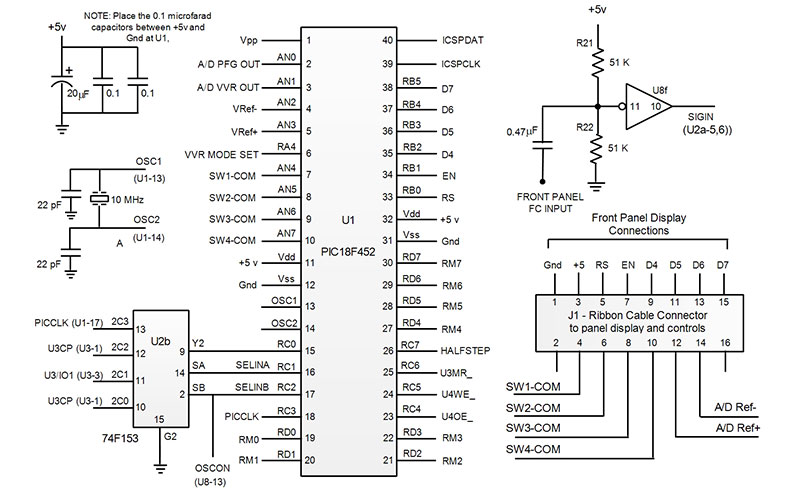
FIGURE 4. Microcontroller schematic.
Its internal clock operates at 40 MHz, giving a 100 nanosecond instruction time. This is important when the frequency counter is operating in the period measurement mode or when you want to implement the PFG directly from the PIC (bypassing the RAM).
Because this PIC has a PLL that multiplies the crystal frequency by four, a 10 MHz crystal can be used. This reduces radiation that might interfere with the frequency counter input amplifier.
The accuracy of the frequency counter is entirely dependent on the accuracy of the crystal. A typical crystal has an accuracy at room temperature of about 100 PPM (parts per million); in other words, one in 10,000.
Many temperature controlled 10 MHz oscillators with one in 1,000,000 or better accuracy are available online at reasonable prices.
High Speed Oscillator
Figure 5 is the schematic for the high speed oscillator.
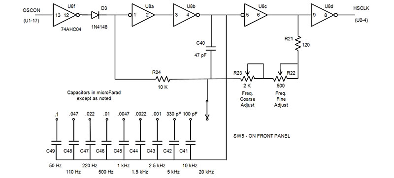
FIGURE 5. High speed oscillator.
It's basically a square wave relaxation oscillator using a 74AHC04 high speed hex inverter that will operate at a maximum frequency of about 15 MHz.
The output (HCCLK) drives the eight-bit RAM clock input in the multiplexer ‘10’ position (the normal PFG mode). At 15 MHz, the output of the PFG with 64-bit resolution is 15,000,000/256 or about 58 kHz.
The output frequency of the oscillator is set by the band switch (SW5) and the two front panel potentiometers R22 and R23. The oscillator is turned off (via SELINB) when in the frequency counter mode.
Software
The software for this project was written in C using the microC development package, but any C compiler would work fine. The commented source code is included in the downloads.
Front Panel
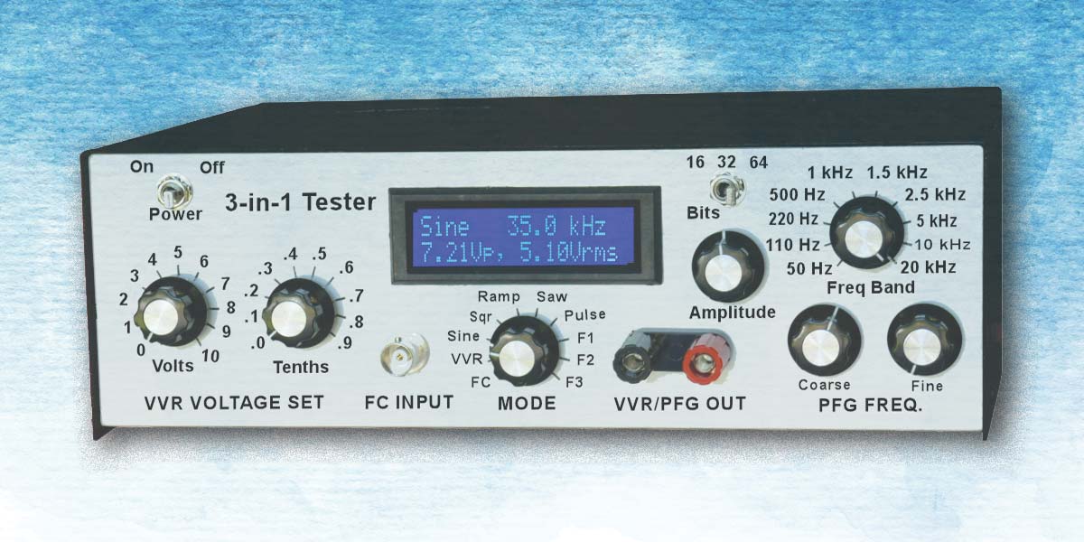
Photo 1 shows the layout of the front panel.
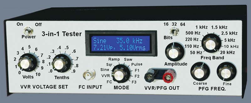
Photo 1.
Figure 6 shows the schematic for the front panel switch and display.
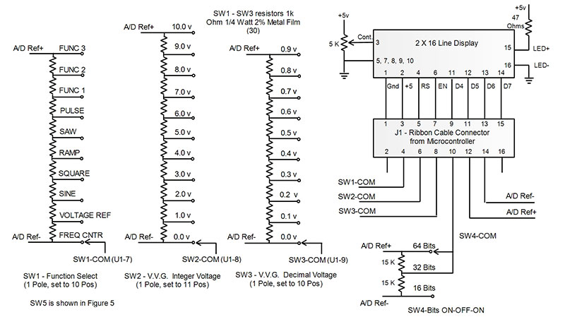
FIGURE 6. Front panel switch and display schematic.
On the left are the two voltage selectors for the VVR: one (SW2) for volts and the other (SW3) for tenth volts. The output of the VVR appears on the two banana jacks (VVR/PFG OUT).
On the right of the front panel are the PFG controls:
• The Bits selection switch (SW4).
• The PFG amplitude potentiometer (Figure 1, R2).
• The high speed oscillator frequency band switch (SW5)
• The Coarse and Fine frequency adjustment (Figure 5, R22 and R23).
In the center of the front panel is the Mode selector switch (SW1) used to choose between the frequency counter, VVR, and several other user preprogrammed PFG functions.
Construction
I mounted all the non-front panel components on two solderable prototype boards. The boards each have 1,258 points arranged in a grid much like other popular solderless breadboards.
Construction drawings are included in the downloads.
Parts List
With the few exceptions given in the Parts List, all resistors are 1/4 watt, 2% metal film. I bought one of the resistor assortments listed on eBay, and now have enough resistors for many projects.
All 0.01, 0.1 bypass capacitors are ceramic disc and all capacitors in the microfarad range are tantalum. These can be purchased from Jameco or Mouser. The other capacitors are shown in the Parts List.
I hope you find this unit as convenient and helpful as I do. NV
Parts List
| ITEM |
DESCRIPTION |
| R2 |
5K ohms |
| R3, R4, R7, R8, R15, R16, R18, R19 |
5K ohms, 1/8 watt, 0.1% |
| R5 |
Bourns 3296W, 200 ohms |
| R12 |
Bourns 3296W, 50K ohms |
| R17 |
100 ohms, 1 watt |
| R22 |
500 ohms |
| R23 |
2K ohms |
| U1 |
PIC18F452 |
| U2 |
74F153 |
| U3 |
74F579 |
| U4 |
CY7C128A |
| U5 |
LM358 |
| U6 |
DAC0800 |
| U7 |
LM6181 |
| U8 |
74AHC04 |
| C40 |
47 pF |
| C41 |
100 pF |
| C42 |
330 pF |
| C43 |
.001 µF |
| C44 |
.0022 µF |
| C45 |
.0047 µF |
| C46 |
.01 µF |
| C47 |
.022 µF |
| C48 |
.047 µF |
| C49 |
.1 µF |
| D1, D2 |
LM4040AIZ5 |
| D3 |
1N4148 diode |
| SW1, SW3, SW5 |
Rotary switch, one pole 12-pos set to 10-pos |
| SW2 |
Rotary switch, one pole 12-pos set to 11-pos |
| SW4 |
On-Off-On miniature toggle switch |
| Q1 |
2N6426 |
| K1 |
Omron G5V-2-H1-DC5 |
| LCD display |
16x2 line LCD display |
| Prototype boards |
|
| Cabinet |
|
| Power supply |
Triple output |
| BNC panel mount |
|
| Dual banana jack |
|
| Knobs (7) |
|
Downloads
What’s in the zip?
Source Code
Construction Drawings