In this second of five articles, I will review the circuits in the 555 Timer IC Circuits by Forrest Mims which use the 555 specifically as a simple one-shot (circuits 1, 3, 4, 5, 8, 9, 10, and 13), as well as discuss how to use the PIC 555 replacement discussed in Part 1 in the same applications. I have also included three dedicated one-shot programs that can be modified as required for your own projects. The third program is written using interrupts so that you can embed it within your own program. The third article will discuss most of the circuits which use the 555 as an astable multivibrator in audio applications. The final articles will examine the remaining circuits.
There are several limitations which a PIC (or any microprocessor) implementation will have relative to a 555 (unless there is specific one-shot hardware in the processor):
- With any processor emulation of a 555, there will be a delay between the trigger and the output pulse. The delay will be a multiple of the instruction execution time, plus a fraction of the instruction time due to the phase difference between the triggering edge and the CPU clock edge.
- The available pulse widths will always be a multiple of the period of the CPU clock.
- The power supply voltage is limited to a maximum +5V. Depending on the PIC you are using, the VDD may be as low as 1.8V.
- The output current is limited to 50 mA — sink or source — at least in the PICs which I have been using.
If the first two of these limitations are not acceptable for your application, then you will want to use the 555 itself. If the last two are an issue, an external buffer transistor will handle higher voltage as well as current.
Mims Circuit 1
Circuit 1 in the Mims book is the Basic Monostable Circuit and is redrawn in Schematic 1 for reference.
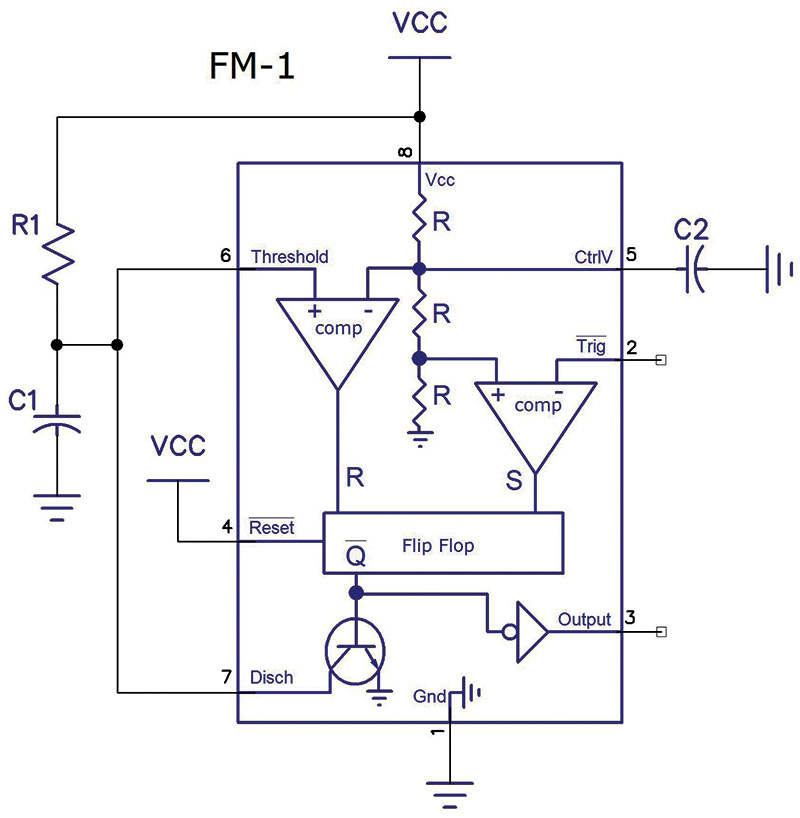
SCHEMATIC 1. Basic 555 monostable circuit.
The formula for determining the output pulse width of a 555 is:
PW = 1.1 * R1 * C1
where PW is in seconds; R1 is in ohms; and C1 is in farads. Or, to make it more practical: PW in milliseconds; R1 in Kohms; and C1 in microfarads.
One of the restrictions of the 555 is that the triggering pulse must be shorter than the output pulse. Otherwise, the output pulse will be as wide as the trigger. This is why many 555 circuits use a capacitor to couple the trigger signal to the trigger input.
Another is that it only triggers on the falling edge.
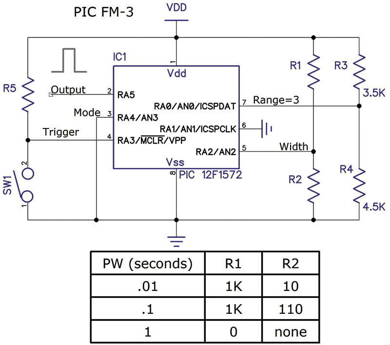
One-shot mode (mode 0) of the PIC 555 replacement is most easily selected by grounding the mode pin (Schematic 2). In all four one-shot modes, the selected transition at pin 4 will trigger the output pulse.

SCHEMATIC 2. PIC 555 replacement, Mode 0.
There is a definition in the program that allows the choice of triggering edge. The pulse width is calculated as follows:
(1) PW = * 1024 * Resolution
where VR2 is the voltage at the center tap of R2 and the Resolution is determined by the voltage at pin 7 of the PIC as described in Part 1. The output pulse width is independent of the triggering pulse width or VDD.
One-Shot Programs
I have written three sample programs demonstrating one-shot operation for the PIC12F1572 processor. The reason for choosing this particular processor is simply that it is the one I have used most recently for one of my projects. Schematic 3 is the test setup I used for the three programs.
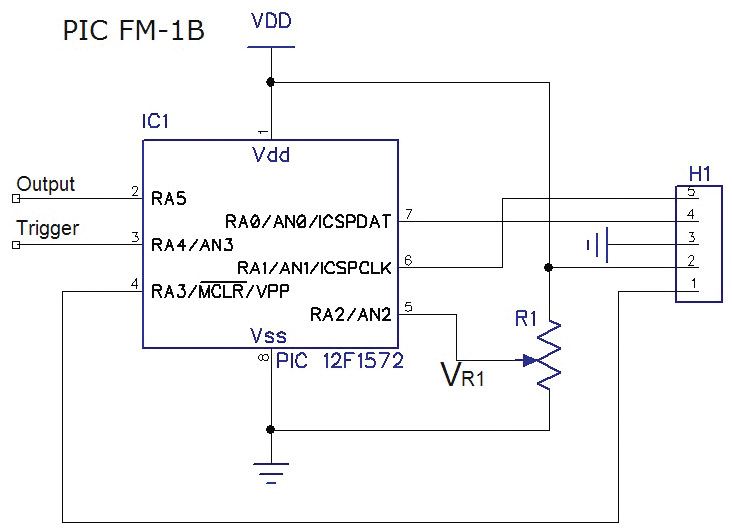
SCHEMATIC 3. Test circuit for the three programs.
Note that it uses the I/O pins a little differently than the PIC 555 replacement in order to allow the programming/debug header to be connected.
The programs (available in the downloads) were written mainly as programming exercises and will benefit those who have not done much assembly language work. I believe they are well documented and should be easy to follow.
I have used some techniques that I believe are good programming practice such as giving symbolic names to constant values and a regular naming convention for those names, as well as subroutine names.
Some of the conventions/ rules I use in my assembly language programs are:
- Constants
Upper case
May use underscores
May not use periods
- Subroutine names
Significant words capitalized
May use periods
May not use underscores
- The name assigned to intermediate locations within a subroutine use the full subroutine name followed by a period and one or more digits.
- Almost every line in an assembly language program has a meaningful comment.
- Sections of code that perform a specific task or subset of a task have a leading comment describing that task.
- Subroutine comments before any code
- Describe the function of the subroutine.
What is necessary to enter the routine: registers, R/W memory, etc.
What memory and/or registers are modified.
Where is the end result of the subroutine stored.
Program 1: MSMV-1 (MSMV = Mono Stable MultiVibrator) demonstrates the simplest and fastest one-shot possible with a PIC. All it does is wait for the selected input to transition, and then generate a pulse using two assembly language instructions to turn an output bit on then off. An outline of the program (other than initialization) might be:
- Wait for the trigger.
- Turn on the pulse.
- Turn off the pulse.
- Go back to (1).
All three programs make use of one of the hardware features of this PIC in order to select the triggering edge: Interrupt-On-Change. This is a feature of the PIC which generates an internal signal whenever the selected input signal transitions. Either or both edges can be detected. Programs MSMV-1 and MSMV-2 do not actually use the interrupt capability, but they do make use of the edge capture hardware in order to determine when a triggering edge has occurred.
There are also equates that allow you to define the I/O ports. The executable code in the main program is only seven assembly instructions.
With the CPU clock running at 32 MHz, the output pulse width is one instruction time long: about 125 ns. Not terribly practical, but it does show one-shot operation.
Program 2: MSMV-2 demonstrates using specific numbers of instruction execution times to generate predictable pulse widths. This program is considerably more complex than MSMV-1. It allows you to set the pulse width by loading a register with a value of up to 255 and then calling either of two subroutines which will delay some number of microseconds or milliseconds.
It is more flexible in that you can program any delay you want within the parameters listed, but it still requires you to change the program in order to change the pulse width. There is also an option to enable a retrigger operation.
Program 3: MSMV-3 is the most complex. It does use interrupts as well as one of the timers. It also uses an external analog voltage to allow varying the pulse width. Since the PIC has a 10-bit A/D, the span of the pulse width is approximately 1000:1 of the programmed range.
There are three sets of definitions which allow you to select the range of adjustment:
- Multiply the A/D reading by a power of two: 1, 2, 4, 8, 16, 32, or 64.
- Two selections of the Timer clock frequency: 8 MHz or 31 kHz.
- Four selections of the Timer 1 prescale value: 1, 2, 4, or 8.
Combinations of these yield quite a few basic ranges for the pulse width resolution/ step size. Using the higher Timer clock frequency (CPU clock/4), A/D multiplier of 1, and Timer clock prescale of 8, the range of pulse width is approximately 10 µs to 1,023 µs with a resolution of 1 µs. The reason the minimum is 10 µs is due to instruction execution time and interrupt latency. There are more comments in the program source explaining this.
Mims Circuit 3
Circuit 3 (Schematic 4) is simply an application of the one-shot driving a device which requires a pulse input. As long as the pulse width is longer than the switch (or relay) bounce time, the switch closure bounce will be masked.

SCHEMATIC 4. Bounce-free switch.
Figure 1 shows what switch bouncing can look like on a typical toggle switch. The left edge of the waveform is the initial switch closure; the right edge is the end of the bounce. The total bounce time is 511 µs.
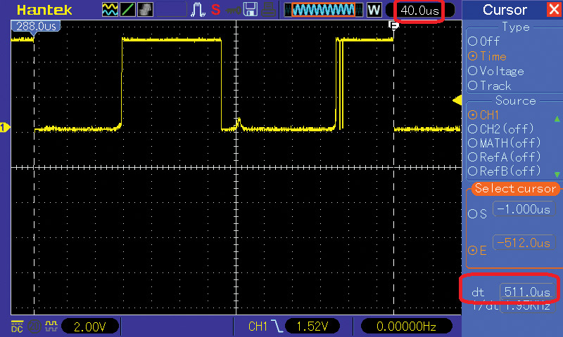
FIGURE 1. Example of switch bounce.
There are some possible issues with this application. As noted earlier, if the trigger signal is low for a time longer than the pulse time, the output will stay high until the trigger goes high.
If the switch bounces upon contact, it will probably bounce upon release which will also cause the 555 to trigger. The best operation of this circuit occurs when the switch closure time is shorter than the pulse width. The PIC 555 replacement can be used as a debouncer (Schematic 5) in much the same way as the 555.
SCHEMATIC 5. PIC 555 bounce-free switch.
Simply set its mode to either 0 (one-shot) or 2 (retriggerable one-shot). The main differences between the PIC and the 555 are that the PIC’s output pulse is not dependent on the triggering pulse width. Plus, you can modify the program to trigger on either edge. However, it will still be susceptible to triggering when the switch opens in the same way as the 555.
If you have a choice of devices to use for debouncing, a better solution is to use a Set-Reset flip-flop and a two-position switch. I have included a schematic (Schematic 6) which shows three simple switch debounce circuits. Circuits 1 and 2 are examples using Set-Reset flip-flops; circuit 3 can use any logic non-inverter.
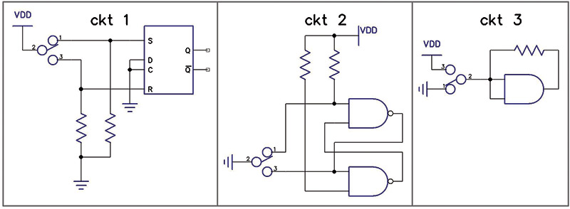
SCHEMATIC 6. Simple switch debouncers.
The purpose of the resistor in the feedback loop is to minimize the amount of momentary current the output has to sink or source when you change the state of the switch. All three of these circuits require a two-position switch of break-before-make construction, which is typical of most toggle switches.
Mims Circuit 4
Circuit 4 (Schematic 7) is a Touch Activated Switch. It activates when your body (acting as an antenna) picks up the 60 Hz power line.
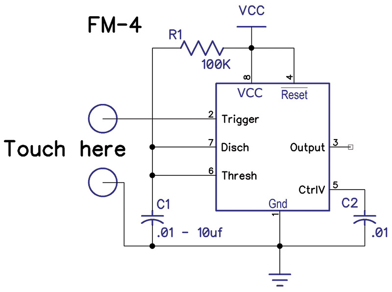
SCHEMATIC 7. Touch activated switch.
With the timing values listed in the book, the pulse width will be between 1 ms (C1 = .01 µF) and 1 sec (C1 = 10 µF). If you use the smaller values of capacitance, you will get a series of pulses out of the 555 at a 60 Hz rate. Depending on your particular application, it might be better to use the 555 as a retriggerable one-shot and set the pulse width to about 20 ms.
The PIC processors I have been using do not have the hardware to use a touch sensitive switch in this way. Several of them do have a capacitive sensing module.
However, the sensing uses the change in frequency of an oscillator to determine when the switch has been closed. This means that your finger is acting as a capacitor to ground instead of an antenna as described above. A method similar to the one in the book can be implemented using either an external op-amp (Schematic 8) or one of the larger PICs which has an integrated op-amp.
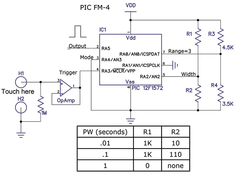
SCHEMATIC 8. PIC 555 touch activated switch.
Mims Circuit 5
Circuit 5 (Schematic 9) is the 555 driving a relay. Within the limits shown earlier, the PIC can drive a relay.
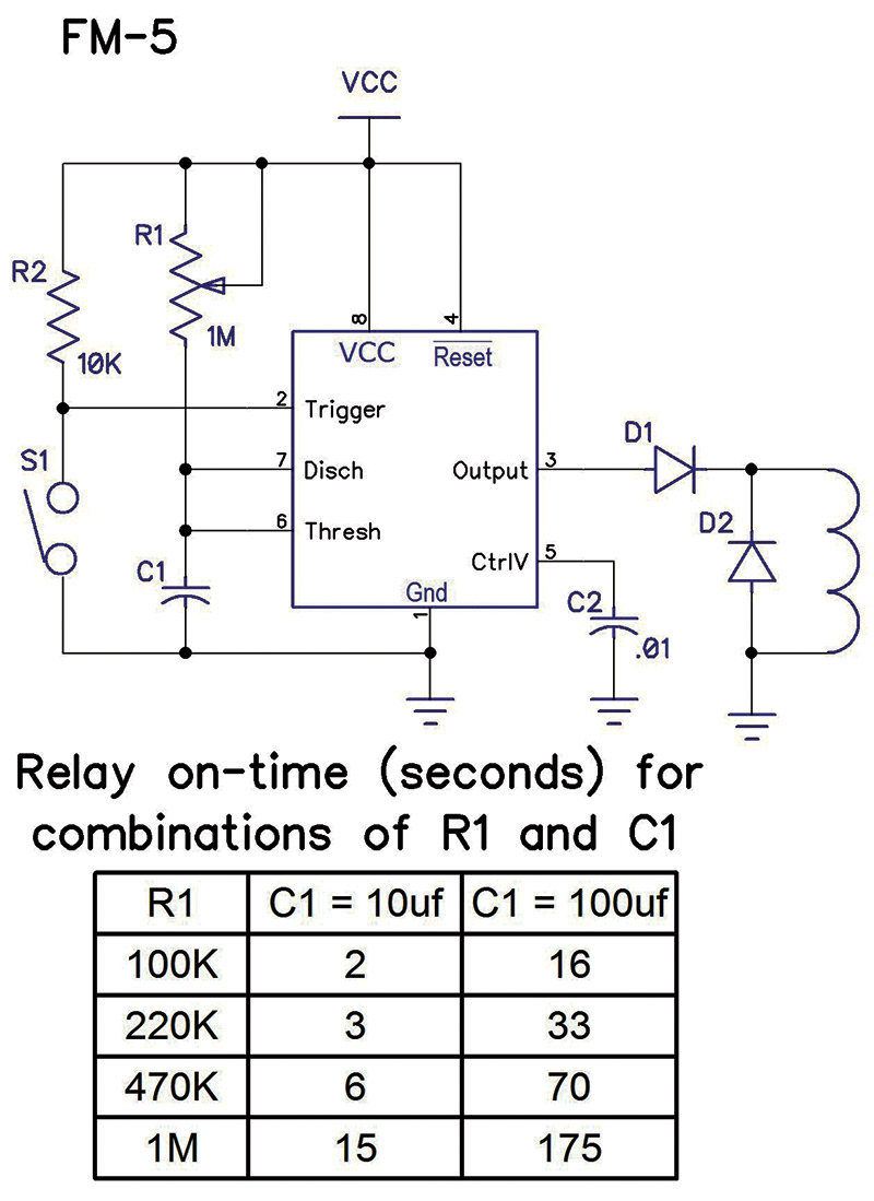
SCHEMATIC 9. The 555 relay driver.
There are quite a few relays which meet these criteria that are in the $1 to $2 price range. If you need to drive a relay that requires more current (>50 ma) and/or requires a higher coil voltage (<=40V), the simple circuit shown in Schematic 10 will do the job. Q1 can be almost any popular NPN transistor (Q1): 2N2222, 2N3904, etc. If you want, you can substitute an FET (Q2) such as the 2N7000.
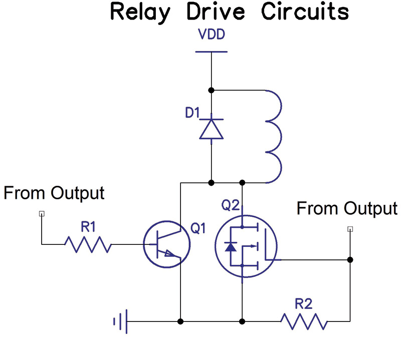
SCHEMATIC 10. Sample relay drive circuit.
In all cases, do not forget the diode across the coil of the relay. It protects the driving device from the voltage spike which occurs when the relay is turned off.
I took scope pictures at the collector of the driving transistor. Figure 2 is one with the diode and Figure 3 is one without the diode.
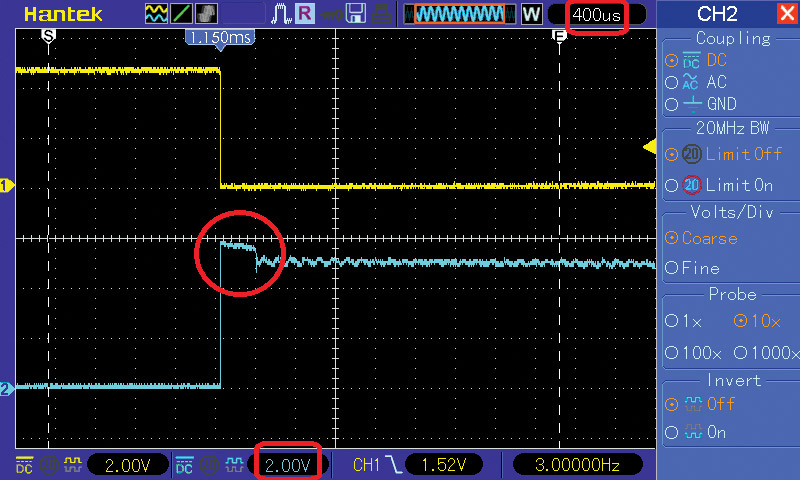
FIGURE 2. Relay drive waveform WITH the diode.
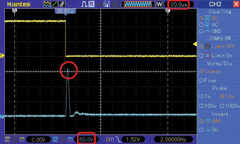
FIGURE 3. Relay drive waveform WITHOUT the diode.
Note the vertical scale on the lower trace in both figures. The one with the diode shows a small plateau when the relay is turned off, while the one without the diode shows a significant voltage spike of about 150V!
Mims Circuits 8 and 9
Circuits 8 (Missing Pulse Detector) and 9 (Event Failure Alarm) shown in Schematic 11 are identical and are retriggerable one-shots.

SCHEMATIC 11. Event failure alarm.
An event failure is essentially the same thing as a missing pulse. As long as the input pulse period is less than the pulse width of the one-shot, the output will remain high (triggered), keeping the buzzer off.
Mode 2 of the PIC 555 replacement is its retriggerable one-shot mode and requires approximately 1.56V on the mode pin if VDD = 5V (Schematic 12).
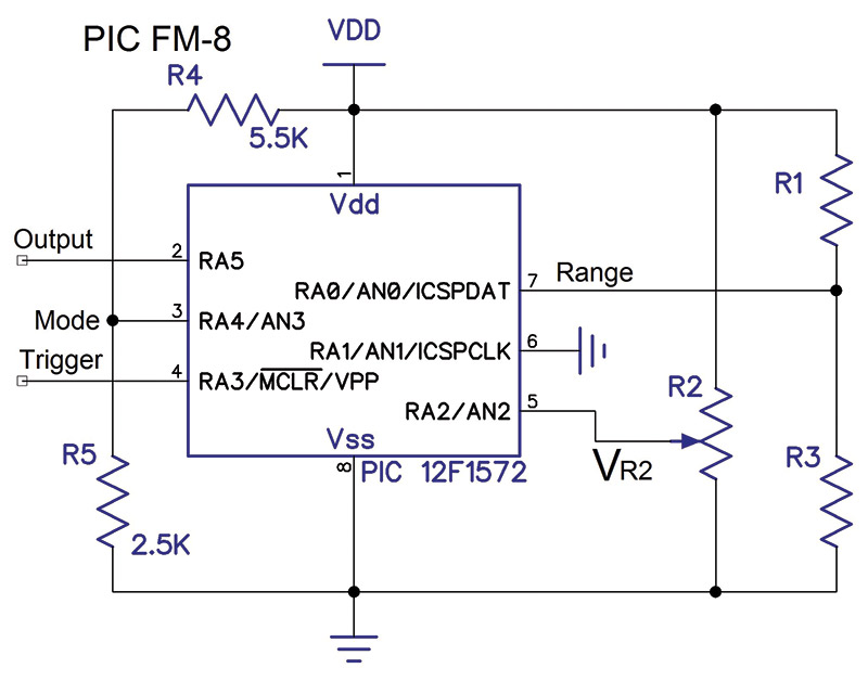
SCHEMATIC 12. PIC 555 missing pulse detector.
One possible shortcoming of these circuits is that when the system is first turned on, the output of the one-shot will be low until the first input signal occurs. In the case of the Event Failure Alarm (FM-9), the piezo buzzer may possibly emit a short tone.
The purpose of transistor Q1 in the 555 circuit is to discharge the timing capacitor each time a trigger signal occurs. This prevents the voltage on the Threshold Input from reaching the Threshold Voltage of 2/3 VCC. This will keep the flip-flop from resetting which keeps the output high.
Notice that in my drawing of Circuit 9, I have added resistor R3. The purpose of this resistor is to keep the discharge current of C1 from being so large that it destroys the transistor. Theoretically, the discharge current through a short circuit from an ideal capacitor is infinite. In any practical circuit, this will never happen, but I still prefer to limit the current through a transistor that is discharging a capacitor.
A piezo buzzer can be added to either circuit between the output and VCC in order to make it into an Event Failure Alarm. Use care in selecting the buzzer because there are two types: internally driven and externally driven. For these circuits, you need the internally driven type.
All they require is a DC voltage applied between the leads, although you do need to be careful because they are polarized.
The externally driven type requires a square wave signal within a specific frequency range. I used one of these in a recent project and drove it from the PWM output of the PIC (Toilet Sentinel, NV October 2016). The externally driven type is generally less expensive.
Mims Circuit 10
Circuit 10 (Schematic 13) shows the one-shot used as a Frequency Divider.
SCHEMATIC 13. A 555 frequency divider.
In order for this to work properly, the pulse width must be longer than the period of the triggering pulses. This type of circuit is inherently limited as to the frequency range over which it will operate. You should use an oscilloscope to adjust the circuit so the pulse width is slightly longer than the period of the lowest frequency signal you want to divide — assuming that you want to divide by 2.
For example, if you set the pulse width to 10 ms, for all frequencies below 100 Hz the output frequency will be the same as the input frequency. For triggering frequencies between 100 Hz and 200 Hz, the output frequency will be half the input frequency. From 200 Hz to 300 Hz, the output frequency will be one-third the input frequency.
Schematic 14 shows my test setup for using the PIC 555 replacement as a frequency divider.
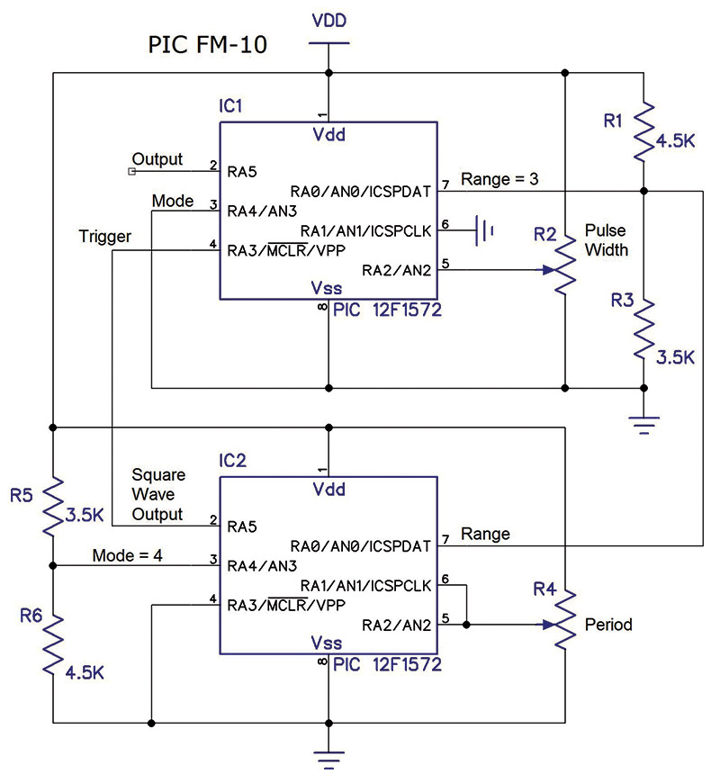
SCHEMATIC 14. PIC 555 frequency divider test circuit.
Both PICs in the schematic are programmed as the 555 replacement. IC1 is set to Mode = 0 which is one of the one-shot modes. IC2 is set to Mode = 4 which is one of the astable multivibrator modes. Both ICs are using Range 3 (1 ms resolution).
Since pins 5 and 6 of IC2 are tied together, both the on time and off time will be the same, thus generating a 50% duty cycle square wave. As long as R2 sets the pulse width of IC1 to be less than the period of IC2, the output pulse of IC1 will fire for every positive transition of the IC2 output; refer to Figure 4.
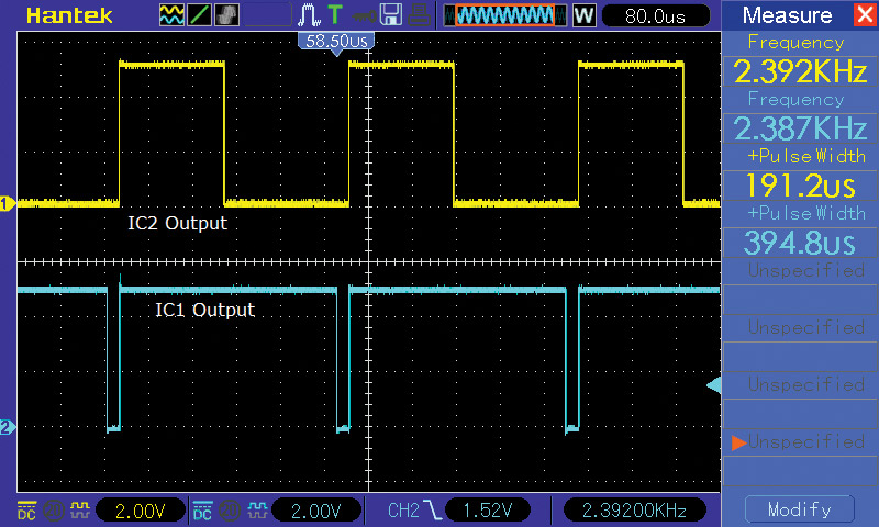
FIGURE 4. Frequency divider — no division.
When the period of IC2 becomes a little less than the pulse width of IC1, IC1 will act as a 2:1 frequency divider (Figure 5). The reason for the “little less” is because of processing delays in triggering the PIC.
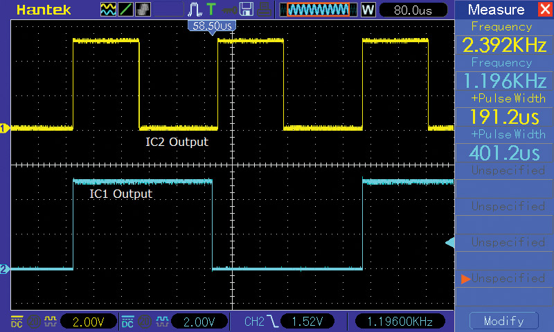
FIGURE 5. Frequency divider — divide by 2.
The upper traces are the trigger signal to IC1 (the frequency divider) which is programmed to trigger on the rising edge of its input, while the lower traces are the output of IC1. When the pulse width of IC1 becomes greater than twice the period of IC2, IC1 will act as a 3:1 frequency divider. This scheme can theoretically be carried out as far as you want. However, the stability of the one-shot as well as its trigger input will become a problem as the divide ratio increases. Also, the range of input frequencies over which the ratio is constant decreases as the divide ratio increases.
Only with a divide-by-2 circuit can you approach a 50% duty cycle from IC1. You cannot get exactly 50% but you can get within 1% with the 555 replacement as long as the output pulse is > 100 times the resolution. The same is true using a 555 except that you will have to use stable components in the timing circuit.
Mims Circuit 13
Circuit 13 (Schematic 15) shows a one-shot used to drive an analog meter for measuring the frequency of the input pulses.
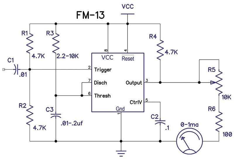
SCHEMATIC 15. Frequency meter.
The pulse width should be a little less than the period of the highest frequency to be measured. The response time of the meter is used to average the stream of pulses that it gets.
This circuit shows a capacitor on its input which is biased to half the supply voltage. Since the other input of the trigger comparator is biased at 1/3 of VCC, the input amplitude must be enough to overcome that difference. It does, however, allow the 555 circuit to be triggered by an AC input.
If you need to measure smaller amplitude signals, you should be able to change the input bias divider so that its voltage is closer to 1/3 of VCC.
The circuit in Schematic 16 uses a 10 mA meter. The pulse width is set to 980 µs so that it can be calibrated to read full scale with a 1 kHz input signal.
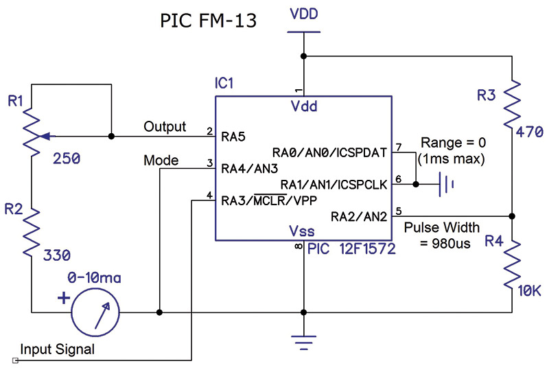
SCHEMATIC 16. PIC 555 frequency meter.
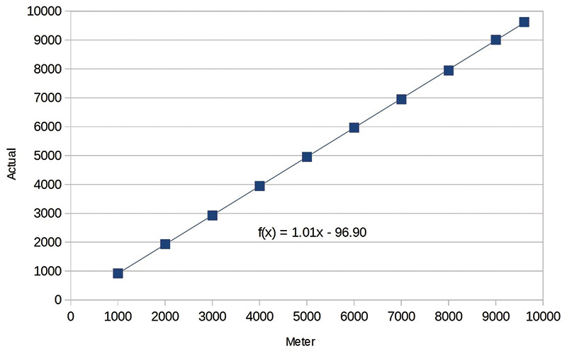
Graph 1 shows the frequency response at 1 kHz full scale. The circuit is quite accurate even though it’s quite simple.
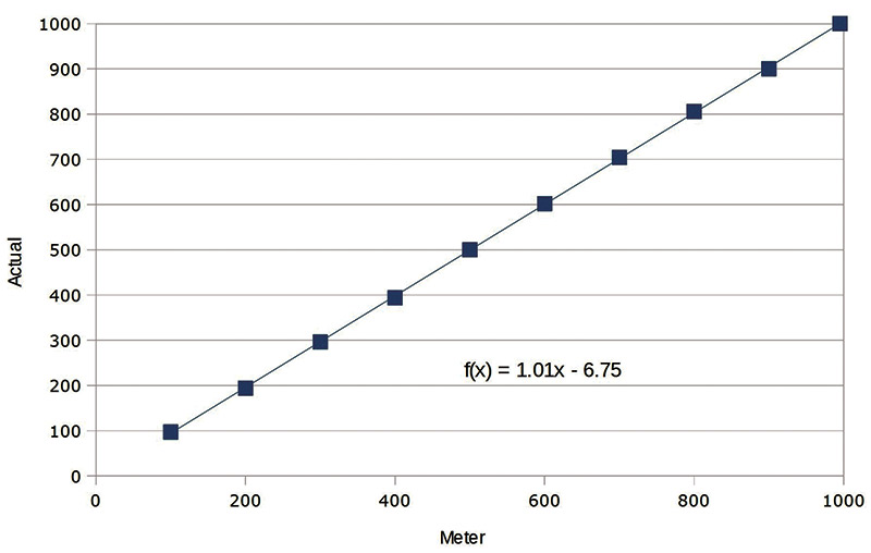
GRAPH 1. A 1 kHz full scale frequency response.
If the input frequency is higher than about 1.02 kHz, the meter reading becomes erratic until the frequency is high enough for the circuit to act as a 2:1 frequency divider, at which time the display will stabilize at half scale.
Graph 2 is the same circuit but with the pulse width set to about 81 µs so it can have a full scale reading of 10 kHz.
GRAPH 2. A 10 kHz full scale frequency response.
One of the reasons why these two pulse widths are not closer to the ideal (1 ms and 100 µs) is because of the trigger delay time of the 555 replacement.
Using a 555 IC would allow you to set the pulse widths closer to those ideal values.
Conclusion
My goal with these articles is to show how a processor emulating a 555 can be used in quite a few different circuits. The Forrest Mims’ book mentioned is an excellent resource for anyone wanting to learn the how’s and why’s of the 555. Using the book as a guide for this article definitely proved to be a very interesting and rewarding task. I hope you have found these circuits as helpful and educational as I have.
The source files for the three sample programs as well as the files for all the schematics are available in the downloads below. I use DipTrace for my schematics and printed circuit boards. NV
Resources
All schematics are drawn using DipTrace
www.diptrace.com
All parts purchased from Digi-Key
www.digikey.com
My website
www.qsl.net/k3pto
Engineers Mini-Notebook 555 Circuits by Forrest M. Mimms, III ©1984.
www.forrestmims.org
Downloads
What’s in the zip?
Source Code
Schematics