When a PIC can Replace a 555
Engineers Mini-Notebook 555 Circuits by Forrest M. Mimms, III ©1984. Also see www.forrestmims.org.
This final article in our series will examine those circuits from the “555 Timer IC Circuits” by Forrest Mims which were not covered in any of the preceding four articles. As in the other installments, some will use the PIC replacement from the first installment (December 2016), while others will develop specific programs using a PIC to emulate a particular implementation of a 555.
Just as a quick review, that first article described a general-purpose 555 replacement using a microprocessor: the PIC12F1572. The second article reviewed the circuits and their PIC equivalents, which used the 555 basically as a mono-stable multivibrator. Part 3 discussed the less complex audio oscillator circuits. The fourth article covered the more complex audio oscillator circuits.
Where I have modified component values in any circuits from the Mims book, I show the original values in parentheses. Also, those components marked with an asterisk (*) are additional components and are not in the original.
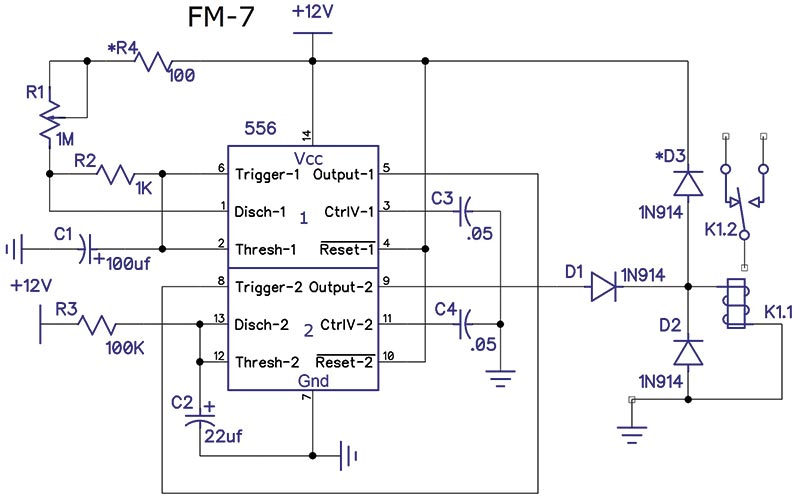
Mims Circuit 6
Circuit 6 in Schematic 1 shows a 555 being used as a cascaded timer.
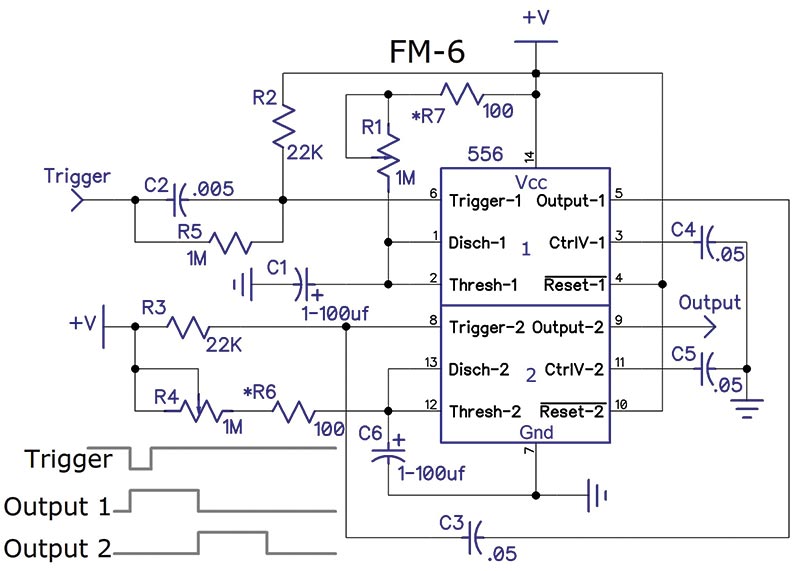
SCHEMATIC 1. 556 cascaded timer.
The output of the first section is used as the trigger for the second section. The trigger for section 1 is essentially capacitively coupled to ensure that the input pulse width is shorter than the output pulse width. Resistor R5 is there to discharge C2; R2 is a pullup that keeps the trigger input high except when the trigger signal transitions to low. The output of section 1 (normally low) is capacitively coupled to the trigger of section 2 which also has a pullup.
The operation is quite straightforward: The high to low edge of the trigger signal causes section 1 to output a positive pulse. At the end of the pulse, the low-going edge triggers section 2. The purpose of the circuit is to generate an output that is delayed from the triggering pulse.
If you need an operation such as this, you can use the PIC replacement in mode 1 (delayed one-shot) or mode 3 (retriggered and delayed one-shot; refer to Schematic 2).
| Mode/Range |
R2 or R4 |
Mode |
Range |
| 0 |
0 |
One Shot |
1us-1ms |
| 1 |
1.5K |
Delayed One Shot |
10us-10ms |
| 2 |
2.5K |
Retriggered One Shot |
100us-100ms |
| 3 |
3.5K |
Retrig & Dly One Shot |
1ms-1s |
| 4 |
4.5K |
Astable: On Time & Off Time |
10ms-10s |
| 5 |
5.5K |
Astable: On Time & Period |
100ms-100s |
| 6 |
6.5K |
Metronome: Beats per Measure & Tempo |
1s-1000s |
| 7 |
open |
(not implemented) |
10s-10,000s |
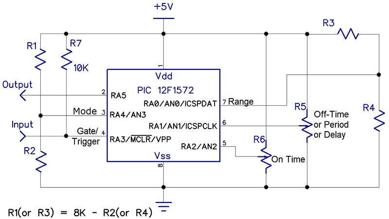
SCHEMATIC 2. PIC 555 replacement.
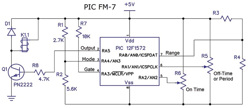
I have also developed a program (MSMVx2.asm) which simulates two 555s as shown in Schematic 3.
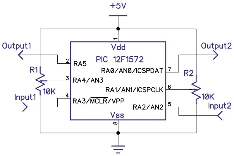
SCHEMATIC 3. PIC dual 555 monostable.
Both one-shots have been programmed to trigger on a negative edge, but this is easily altered by changing either or both of two definitions. It’s also possible to enable the one-shots to trigger on both edges, but the program would need to be modified a little bit. There are definitions that enable the one-shots to be retriggered.
Both monostable multivibrators (one-shots) use one of the timers in the PIC to determine the pulse width. One-shot 1 uses Timer 0 and one-shot 2 uses Timer 2.
Both one-shots have approximately a 1000:1 pulse width span due to the 10-bit A/D (analog-to-digital) converter. There are definitions in the program which enable you to change the resolution (also changes the minimum and maximum widths) of the pulses.
Mims Circuit 7
Circuit 7 (which is shown in Schematic 4) is titled as an intervalometer. It’s simply a 556 with section 1 wired as an astable and section 2 as a monostable driving a relay. The period of section 1 determines how often the relay is activated, while the pulse width of section 2 determines the length of time the relay is activated.
SCHEMATIC 4. 556 intervalometer.
The timing diagram in the book has the output of section 1 inverted. The output should be shown as high for most of the time with a short low pulse. Also, the 555 (in monostable mode) is triggered on a negative-going edge which the diagram would show if the upper trace was to be inverted.
The diodes are for protection against the high voltage inductive kick which occurs when the relay is turned off. D1 prevents it from reaching the 555, while D2 should prevent the voltage across the coil from exceeding the reverse breakdown voltage of the diode. I believe a better placement for D2 would be what’s shown by D3 in Schematic 4. This would clamp the high voltage to one diode drop above the power supply.
The operation of this circuit can easily be obtained using a 555 replacement in either mode 4 or mode 5. Schematic 5 shows the wiring of the 555 replacement for this equivalent circuit (the resistor values are for mode 5). Note that the PIC uses a transistor buffer to drive the relay.
SCHEMATIC 5. PIC 555 replacement for the intervalometer.
The PIC output current is limited to 20 mA, so a buffer is going to be required for most relays. Select mode 4 if you want to control the off-time of the relay and its on-time. Select mode 5 if you want to control the period of the relay operation and its on-time. This is a subtle difference but may be important depending on the application.
Also, note that the 555 circuit uses +12V while the PIC should use no more than +5V. A higher voltage relay can be used if desired simply by connecting the “top” side of the relay and cathode of the diode to the required voltage.
Mims Circuits 12, 22, and 23
The circuits in Schematic 6 use the 555 as a simple pulse generator. For FM-22 and FM-23, the only differences are the loads the 555 is driving and the timing components.
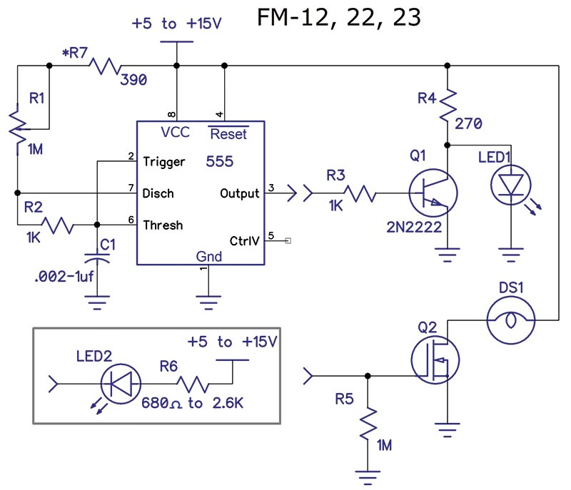
SCHEMATIC 6. 555 pulse generator.
Its astable operation has been discussed in previous articles of this series, so I won’t repeat it here. The frequency range of FM-12 is roughly 1.4 Hz to 300 kHz depending on the capacitor. I have included a spreadsheet with the article downloads (555 Astable.ods) which calculates the time values based on the three timing components. Keep in mind that as R1 becomes small, the circuit will stop operating correctly (if R7 = 0).
I found that with C1 = .01 µF or .1 µF, I needed to make R7 about 390 ohms for the circuit to work properly with R1 = 0 and VCC = 5V. Each capacitor value yields about a 400:1 frequency span.
With this circuit, the output is a very narrow low level pulse. For any given range determined by the capacitor, the output pulse width will be fixed unless you vary the value of R2. The following formulas apply:
LowPulseWidth = ln(2) x R2 x C1 = .693 x R2 x C1
Period = ln(2) x (R1 + R7 + (2 x R2)) x C1
Due to component tolerances — especially the capacitor — you can use either 0.66 (2/3) or 0.7 instead of the constant shown in the equations, which will get you close enough for the vast majority of applications.
The values shown in the schematic are specifically for FM-12, the pulse generator. For FM-22 (an LED flasher), R1 is 100K and C1 is 47 µF. The flash rate can be varied between 0.2 Hz and 8.3 Hz. The 2N2222 inverts the signal and causes the LED to flash on for a short time (when pin 5 is low) of approximately 32 ms.
Since the 555 has plenty of drive capability that can easily handle an LED directly, it’s possible to get the same results without a transistor using the alternate LED circuit shown in the box. The value of R6 (as well as R4) should be calculated based on the supply voltage and the current required by the LED. The values shown for R6 cause about 5 mA through LED2 at the two voltage extremes.
Just as a note of interest, the original circuit with the transistor draws roughly the same amount of current independent of the state of the LED. The alternative circuit (without the transistor) draws very little current when the LED is off.
FM-23 is a power FET lamp dimmer (using R5, Q2, and DS1) with R1 = 1K or 5K and C1 = .047 µF. Here again, the output low time (Q2 off) is fixed; this time, at about 32 µs. This implementation also has a fixed resistor of 390 ohms in series with the potentiometer allowing the pot to be adjusted to zero ohms (without damaging the 555 or causing the circuit to malfunction). This will yield close to a 50% duty cycle.
The frequency is high enough so that the lamp appears to be on continuously at varying levels of intensity. However, since the duty cycle is limited to a minimum of 50%, you will not be able to dim it to completely off. Strictly speaking, R5 is not necessary, but I prefer to not have the gate of an FET floating while the circuit is being assembled.
In general, a PWM circuit operates with a constant period while both the on-time and off-time changes. With this circuit, the off-time remains constant while the on-time and period are changing so that longer periods produce higher duty cycles. In both cases, it’s the duty cycle that is important. The higher the duty cycle (longer output high time), the brighter the bulb.
The circuit of Schematic 2 can be used as the basis for all three of the above circuits using either mode 4 or 5. It has the advantage of allowing independent modification of both the on-time and off-time (or period), and its duty cycle can span 0.1% to 99.9%. The table in the schematic shows the resistor values required for different ranges and modes of operation.
Just a note for the lamp dimmer: Frequencies above 60 Hz are usually not noticeable by most people.
A recent project I did used PWM to drive a DC fan motor. Schematic 7 shows the driver circuit I implemented.
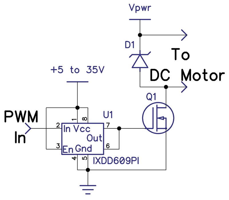
SCHEMATIC 7. FET gate driver.
I used the circuit of Schematic 2 and this driver to get a very smooth speed control. I set the PIC 555 replacement to mode 5 with a period of about 30 µs. The reason for the relatively high frequency was due to the type of motor being used. Lower frequencies tended to make the motor chatter.
The IXDD609 is a FET gate driver and is required to overcome the gate capacitance of the FET. Without this driver, the gate input rise and fall times were slow enough that the FET turned on and off slowly and became quite hot. With the driver, the FET doesn’t even get warm when driving a five amp motor at full speed.
There is one caution: The supply voltage to the IXDD — or whatever FET driver you use — must not exceed the maximum VGS of the FET (or the max voltage of the driver IC), while still being high enough to ensure full turn-on of the FET.
I used a Schottky diode because they are faster than a normal power diode and they have a lower forward voltage drop yielding lower power dissipation. In this application, the diode gets hotter than the FET. I put both the diode and the FET on heatsinks.
Mims Circuit 24
The light/dark detector shown in Schematic 8 uses a photoresistor connected to the Reset input as a gate for the 555 wired as an astable multivibrator.
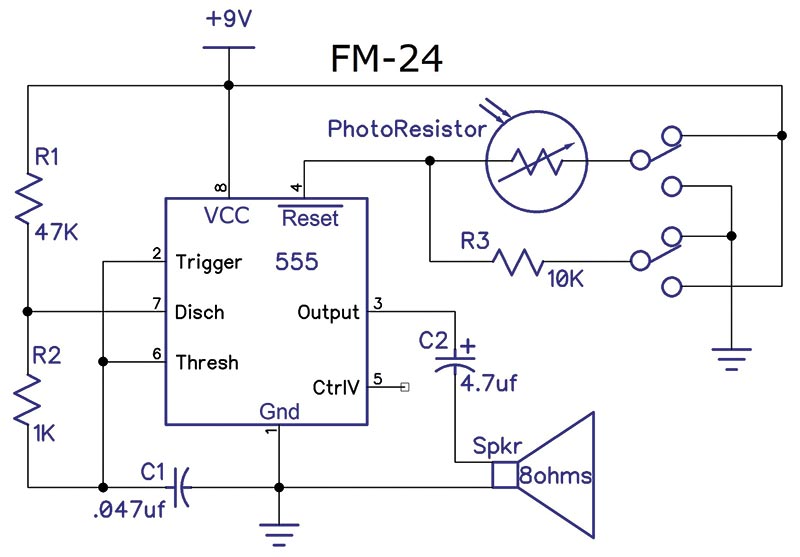
SCHEMATIC 8. 555 light/dark detector.
The Reset input has to be high in order for the 555 to oscillate. The position of the switch determines whether the 555 is enabled when light hits the photoresistor (lower resistance when exposed to light) or does not hit it.
The threshold of the Reset input is about 1V but the input resistance will be different depending on the semiconductor process used for the part: MOS versus bipolar. Using an MOS part (input current about 10 pa) allows you to pick a photoresistor with higher on and off resistances. If you are using a bipolar part, you will need a photoresistor with lower resistance values and you may need to make R3 smaller.
You can use the circuit of Schematic 2 for this application as well, with either astable mode (4 or 5). The same photoresistor circuit can also be utilized to drive the gate/trigger (RA3) input.
Mims Circuit 25
Schematic 9A is an infrared security alarm. U1 is configured as an astable multivibrator with a frequency of about 6 Hz, period = 166 ms. The LED will be turned on when the output is low; about 3.2 ms. U2 is configured as a monostable multivibrator (one-shot) with an on-time of almost 52 ms.
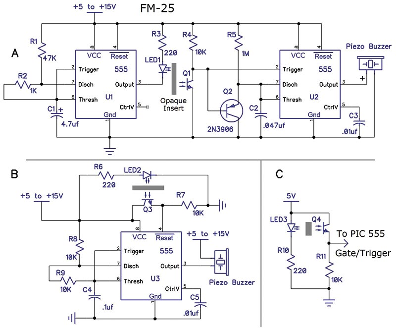
SCHEMATIC 9. 555 infrared security alarm.
With the insert in place, Q1 will be off which causes Q2 to be held off and the trigger input of U2 is held high. With the trigger high, the output will be low keeping the buzzer turned off. When the insert is removed, U2 will be triggered as well as Q2 turning on synchronously with the output of U1 causing the one-shot (U2) output to go high.
Capacitor C2 will charge until it reaches the threshold voltage at which time the output will turn off and the discharge circuit will turn on. The buzzer in this circuit must be of the internally driven type.
Since I was unsure of the function of Q2, I tested the operation of this circuit by driving the U2 trigger circuit directly from a PIC 555 in mode 4, range 2, and off-time of about 3 ms.
When the trigger goes low (simulating the insert being removed and LED1 turning on), U2 is triggered, Q2 turns on, the 555 discharge circuit turns off, and the buzzer turns on for the duration of the C2 charge cycle.
With the component values shown, the removal of Q2 has no impact on the circuit. The output low time of U1 is short enough (3.3 ms) that Q2 does not affect the charging of C2. If the U1 output low time is increased to 6 ms or greater, then Q2 begins to have an effect on the charge time of C2; see Picture 1.
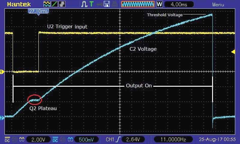
PICTURE 1. 555 astable capacitor charge cycle.
The area circled in red shows the plateau caused by Q2 which is clamping the capacitor to about 0.5V. Since the plateau does not start until about 5 ms after the trigger, it will not occur with a trigger pulse width less than 5 ms.
Once the trigger is removed, Q2 will turn off allowing C2 to finish charging to the threshold voltage and turn off the output.
Schematic 9B shows another possible implementation. This one is similar to FM-24 in that the Reset input is used as a gate for the astable multivibrator.
I also changed the operation such that the frequency of the 555 is about 500 Hz so that the buzzer needs to be of the externally driven type. In this case, the buzzer will sound continuously when the insert is removed.
If you want a pulsing sound, then you should change the timing components (R8 = 47K, R9 = 15K, C4 = 4.7 µf) and use an internally driven buzzer.
You can easily use the PIC 555 circuit of Schematic 2 for this application. Use the circuit shown in Schematic 9C to drive the MCLR input and use mode 4. You can set the circuit to either have a continuous tone or a pulsing tone just as described for the 555 implementation in the previous paragraph.
Mims Circuits 26 and 27
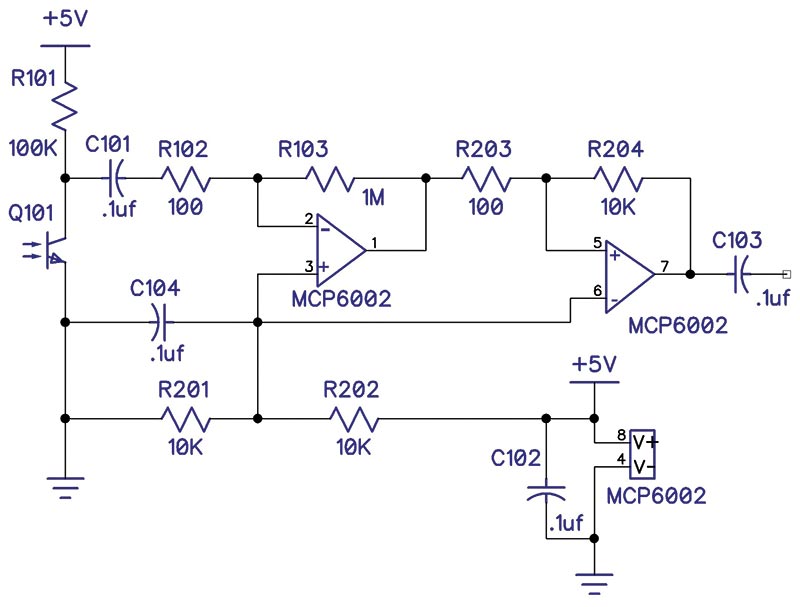
The two circuits shown in Schematic 10 are an analog lightwave transmitter and receiver.
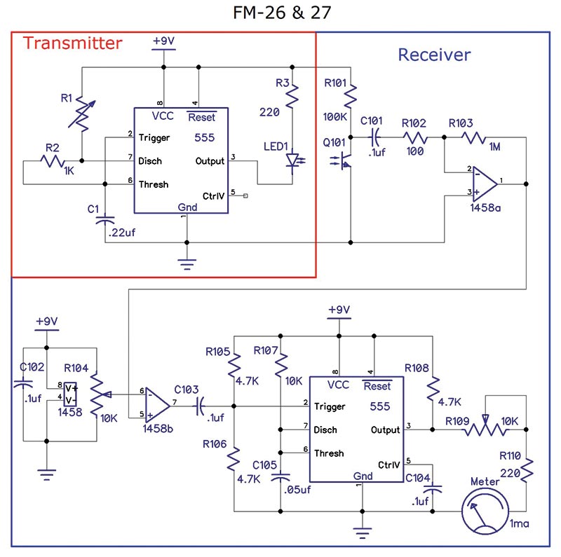
SCHEMATIC 10. 555 analog lightwave transmitter and receiver.
The transmitter circuit is a simple 555 astable multivibrator whose output period varies with the value of R1. If you use a photoresistor for R1, the frequency will vary with the amount of light hitting it. The higher the light intensity, the lower the resistance which yields higher frequencies.
The 555 portion of the receiver is identical with a few minor component value differences to the frequency meter of FM-13 discussed in Part 2 of this series. The op-amp is there to amplify the signal from the phototransistor so that relatively weak signals can be handled. The op-amp circuit can be eliminated if the transistor is close to the IR diode.
The operation of the circuit is such that the meter — when calibrated with R109 — will show the frequency of the transmitter pulse stream. R104 is used to adjust the trip point of 1458b which is being used as a comparator.
There is one minor issue with the circuit: The 1458 specifications state that the minimum voltage between the power pins is 10V. The circuit will probably work at 9V, but it could be marginal. The text in the book suggests that 741s may be substituted for the 1458; however, the 741 specifies a minimum supply of ±10V or, if used with a single supply, 20V.
Schematic 11 shows an alternate op-amp circuit. The basic circuit is the same except that the op-amp has been replaced with one of the many rail-to-rail op-amps available today which were not available when the Engineer’s Workbook series was written.
SCHEMATIC 11. Alternate op-amp buffer.
This circuit has two additional features for section 2 of the op-amp: no potentiometer required for setting the trip point; and some hysteresis (about 100 mV) for a little noise immunity. The op-amp shown has a maximum supply voltage of 6V. However, there are many single voltage rail-to-rail op-amps that have a wider supply voltage range which will also work in this circuit.
Two PIC replacements can be used instead of the 555s. Use the table shown back in Schematic 2 to select the appropriate modes, range, and pulse characteristics. For the transmitter (as with the 555 implementation), the output period can be controlled by a photoresistor as one leg of a voltage divider.
However, with this circuit, you can just as easily drive the off-time input from a voltage source. For instance, you could use a photocell whose output voltage varies with light intensity.
Schematic 12A is an example of the transmitter using a PIC 555 replacement and a photocell. The circuit is essentially a VCO with a 50% duty cycle. The placement of the photocell may look a little strange, but keep in mind that lower voltages on the control inputs correspond to lower period values, i.e., higher frequencies.
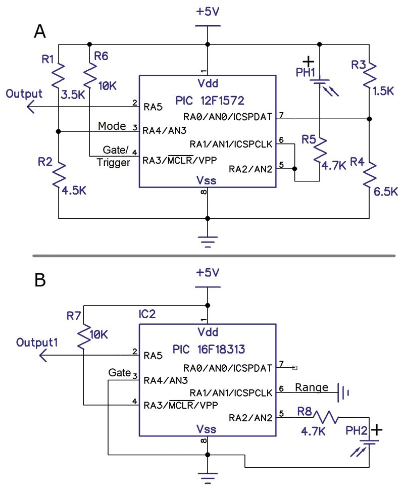
SCHEMATIC 12. PIC analog lightwave transmitters.
Putting the positive terminal of the cell on the +5V line will cause the control voltage to decrease with higher light intensity which will then yield higher frequencies.
Schematic 12B shows a similar circuit using the NCO feature of a PIC18313. (See Part 3 of this series for sample programs.) In this case, however, higher voltages on the control input cause higher frequencies on the output.
In both cases, you’ll want to make sure that the maximum output voltage of the photocell is less than 5V. Resistors R5 and R8 are there to limit the current to the inputs in case of excessive photocell voltage.
For those of you who like a programming challenge, you can edit MSMVx2.asm and modify it so that one section is an astable multivibrator and use it to drive the IR transmitter. The other section would stay as a monostable to be used as the receiver.
Mims Circuit 28
The last circuit in the book (Schematic 13) is a DC-DC converter. It uses a 555 in its astable configuration at about 2.9 kHz with a low pulse width of about 7 µs. This is very close to a 98% duty cycle.
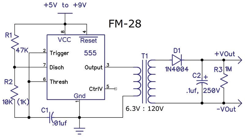
SCHEMATIC 13. 555 DC-DC converter.
In my experimenting with the circuit, I found that I could not even get close to Mr. Mims results using the values and configuration in his schematic. I had to make some changes to get nearly the same results.
I used a different transformer which would have affected my results. Refer to Schematic 14 for my final 555 circuit.
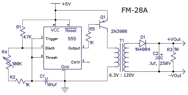
SCHEMATIC 14. Modified 555 DC-DC converter.
The first problem I found with the original circuit was that the 555 was getting quite hot. I believe this was due to the very high duty cycle of the configuration and that the 555 output was driving a transformer connected to ground.
This meant that the 555 output was essentially shorted to ground for 98% of the time. I first simply moved one side of the transformer to +V which corrected the heating issue, but I still didn’t get as high a voltage.
The second change I made was to increase the value of R2 to 10K. With the 1K in the circuit, I measured about 50V across C2 (with Vcc = 5V). With 10K, I measured about 80V.
The last changes were to insert a PNP buffer between the 555 and transformer and then insert a 100K potentiometer in series with R2. These two changes allow me to adjust the voltage from about 10V to over 100V with a 5V supply.
Replacing the 555 in Schematic 14 with the PIC 555 will yield similar results. Use mode 5 and range 0 with a fixed frequency of about 2 kHz.
With a 100K load, a duty cycle of 90% yields about 23V, while a duty cycle of 50% yields 70V.
Lower duty cycles don’t give much higher voltages. Keep in mind that the PIC duty cycle is based on the ratio of output on (high) to period. With the PIC output on, the 2N3906 is off.
That’s a Wrap
I have enjoyed writing this series and would like to thank Nuts & Volts for asking me to write it. I’ve learned quite a bit about the 555 and its many uses from reading and implementing the circuits described in 555 Timer IC Circuits by Mr. Mims and hope that you have as well.
If you have any questions about the PIC 555 replacement or any of the examples in this series, feel free to email me at [email protected]. NV
Resources
All schematics are drawn using DipTrace
www.diptrace.com
All parts purchased are
from Digi-Key
www.digikey.com
My website
www.qsl.net/k3pto
Downloads
What’s in the zip?
Schematics