This article discusses basic theory on the decibel unit and its role in electrical measurements of power, etc. It also describes the construction of an RF power meter which in the past has been difficult to use and expensive to own.
When I first started out in my electronics career, I detested the decibel or anything connected to it. Like most people, I liked linear relationships and multiples of ten. They just seemed to be so much easier to visualize in my mind than logarithmic ratios and terms that I never seemed to find a good use for. However, as time went by, decibels were starting to appear everywhere: audio, radio frequency, and semiconductor datasheets to name a few. Grudgingly, I forced myself to accept and work with them. In the coming years, I grew to love them because they really boil a lot of math down to simple arithmetic.
So, what is a decibel? As the prefix implies, it is one tenth of a Bel which now begs the question, what is a Bel?
Alexander Graham Bell (the inventor of the telephone) did a lot of research work on sound wave intensity as related to the human ear. He determined that loudness was perceived in a logarithmic fashion rather than a linear one. Through many tests, he set up a standard of units as to the range that the human ear can detect — from barely audible to the threshold of pain.
Each unit was a doubling of loudness of the previous unit as the human ear perceived it, yet each unit required a tenfold increase of sound wave intensity relative to the previous unit to achieve that. Starting with a pin drop, all the way to the threshold of pain — and if memory serves me right — there were 13 different levels of these units, ranging from barely audible to excruciating painful.
So, 13 units is about 8,000 times louder than the threshold of hearing as far as the human ear is concerned (0 to 130 decibels). However, the actual magnitude of sound wave intensity over this same range is a ratio of over a trillion to one. The ear adjusts accordingly so that our head doesn’t ‘explode.’ What a remarkable sensor it is!
The term Bel wasn’t really established until some years later when early Bell Telephone engineers renamed TUs (Transmission line Units) to the term ‘Bel’ in honor of Alexander Graham Bell. However, Bels were too large and cumbersome to work with when applying it to “new technology” and they needed greater resolution of measurement.
Soon the term deciBel (dB) became the preferred function to work with and almost completely erased the term Bel from specs and math. However, the term Bel still has validity, and if you want to drop some jaws, the next time you are discussing a particular amplifier’s gain with your cohorts, instead of saying it has a gain of 30 deciBels, tell them it has a gain of 3 Bels. A perfectly valid (although unpopular) term. Then walk away and see who figures it out first!
Even though the decibel emanated from Ma Bell, it was not long before it spread like wildfire in the scientific community. These days, it’s used everywhere and with dozens of suffixes to denote particular values and references; to name a few: dBm, dBW, dBV, dBc, and the list goes on. For this article, we’ll only concentrate on dBm, but even that needs some clarifying.
The term 0 dBm actually has a valid power level and denotes a reference power level of one milliwatt dissipated in a given load; strictly speaking, it should be followed with a load impedance value. The most popular are dBm-50, dBm-75, and dBm-600, which refer to RF, cable, and audio in that order. The RMS voltages at these power levels are approximately 0.224V, 0.274V, and 0.775V, respectively.
Again, all dBm levels start at zero which is the reference point of one milliwatt. I’ll be working with dBm-50 for the rest of this article, and since I’ll be dealing strictly with RF, it will be assumed that it’s in a 50 ohm environment and dBm will suffice.
For starters, one point must be made perfectly clear: dB and dBm are two different terms and each should be used in its proper place. dB has no value at all and only indicates a mathematical ratio. dBm has an absolute value and is not a mathematical term per se. The term zero (0) dBm may seem strange at first, but this sets the reference point by which all other values of dBm are referred to:
So, what is a decibel? As the prefix implies, it is one tenth of a Bel which now begs the question, what is a Bel?
plus dBm (gain) for values above zero and minus dBm (loss) for all below zero. Even though it’s stated as “0,” it does have an absolute value of one milliwatt into a 50 ohm impedance, 0.224 volts RMS or 632 mV P-P.
There are two common formulas for the conversion of linear ratios to dB: [10x log of (power level 1/power level 2)] or [20x log of (voltage level 1/voltage level 2)]. Remember that these are ratios only and do not hold any absolute power quantity.
The two formulas given are valid for any load impedance, as long as the impedance is the same for both levels. They are also somewhat interchangeable as by simple Ohm’s Law. If you know the power ratio, then the voltage ratio is the square root of that ratio. If you know the voltage ratio, the power ratio is the square of that ratio (i.e., doubling the voltage quadruples the power).
Even though I use dBs a lot, I only use the math when determining power gain across level 1 and level 2 where each has a different impedance. What I do use religiously are decibel charts.
I like the ones that show 0.1 decibel ratios up to 10 decibels, and then unit ratios up to 20 decibels in 10 db steps beyond that. Nowadays, most of the time, I see a close ballpark figure at first glance — whether dbs or dBms. A quick check of the chart (if necessary) is all that is needed to get a figure within 0.1 dB.
I won’t dwell on the math beyond what I have shown due to the wealth of information on the Internet of this subject, so you can take it as far as you would like to go. A very good source for this is a Rhode & Schwarz write-up, “dB or not dB?” which is available in the article downloads.
To gain a quick rundown on this subject and a little appreciation for it, take a look at Table 1 and try to memorize it. This will become intuitive the more you work with it.
Alexander Graham Bell (the inventor of the telephone) did a lot of research work on sound wave intensity as related to the human ear.
Note that the ratios in Table 1 are only a close approximation and are showing gain. To show loss, just add minus signs in front of them. Also, you can see more clearly the square/square root relationship between voltage and power for any given decibel ratio.
| Voltage Ratio |
Decibel |
Power Ratio |
| 1.0 |
0 |
1.0 |
| 1.12X |
1 |
1.25X |
| 1.4X |
3 |
2X |
| 2X |
6 |
4X |
| 3.16X |
10 |
10X |
| 10X |
20 |
100X |
| 31.6X |
30 |
1000X |
| 100X |
40 |
10000X |
TABLE 1. Key numbers to remember.
After using dBs and dBms for a while, these figures will become quite intuitive also. One nice feature of dBs is that power multiplication and division is done just by simple addition or subtraction of two figures. Also, they reduce linear values of long strings of numbers that can be either side of a decimal point, down to a simple three or four digits.
Most of the time, the term dB is used to spec out parameters such as gain, loss, etc.; dBm, on the other hand, is used mostly for results as to absolute power levels. Let me give a few examples that may make their use a little clearer:
(1) A cascaded string of three amplifiers has individual power gains of 13 dB, 16 dB, and 27 dB. What is the overall power gain? Answer: 13 +16 + 27 = 56 dB total gain. If we use the basic chart in Table 1, we can break 56 down to 40, 10, and 6 dB increments, then linearize it: 40 dB = 10000x; 10 dB = 10x; and 6 dB = 4x.
Remember that these stage gains are being multiplied, so we just add the dB values and multiply the linear equivalents: 10000 x 10 x 4 = 400,000 for the power gain. Since the voltage gain for these same ratios is always the square root of the power gain, it’s 632.5. If you were only interested in voltage gain, you could use just the voltage ratios from Table 1.
Once you’ve worked with these terms for a while, it’s so much quicker and easier to work in dBs and get close approximation answers about as quickly as you can read them.
(2) A string of attenuators that total 19 dB of loss is inserted between two amplifiers with gains of 16 dB each, and then drives a 50 ohm terminated transmission line with a 3 dB loss. A signal level of 13 dBm is coupled into the first amplifier. What is the power level in milliwatts at the end of the terminated line?
For this example, we’ll first take the longer linear way to get the answer (going point to point): 16 dB amp gain = 40x; 19 dB (x80) attenuator and cable loss (which we can invert and show as gain) = 0.0125x; 16 dB amp gain = 40x and 3dB (x2) line loss (again, invert and show as gain) = 0.5x.
So, 40 x 0.0125 x 40 x 0.5 = 10. Then, 10 x 20 mW (which is the 13 dBm input signal) = 200 milliwatts = answer. Again, notice I entered the losses as gains here, so I didn’t have to deal with negative signs.
Now, for the simpler way: 16 dB - 19 dB + 16 dB - 3 dB = 10 dB — which is a 10x increase of the 13 dBm input signal = +23 dBm = 200 milliwatt = answer!
This last method was done in my head in no time flat as per Table 1.
If you’re wondering how I determined the 13 dBm input signal was 20 mW, then just refer to Table 1 and break down 13 dBm into two parts: 10 dB (10x) and 3 dB (2x) =20x; 20 x 0 dBm (1 mW) = 20 mW.
All the preceding was not meant to be a course on the decibel, but rather an introduction of the basics so you can better understand the workings and construction of RF power meters, which the remainder of this article will now discuss.
Background and Construction
I think that most RF engineers would agree that accurate measurement of RF power levels is one of the more difficult measurements to achieve, and they’ll get no argument here.
I have used several commercial power meters over the years, depending on the company I worked for at the time. Most of these were HP, which seemed to have a corner on the market due to years of R&D in that field. They were quite reliable and required a special probe head that measured power by the RMS heating effect produced from the detected signal of measurement.
Because they measured by the heating method, they were oblivious to wave shape and duty cycle. (This method is far superior to any other type of detection.) They had an internal calibrator, and some used a small look-up table for probe zeroing before each session of testing.
In order to rely on their accuracy, they did require a yearly calibration check from a certified metrology lab if measurement records were required for government documentation. However, they seldom went very far from their original specs other than units that had been abused.
These were extremely accurate units with very high price tags and, in general, had a 40 dB range of measurement; usually -20 dBm to +20 dBm. I had always drooled over the thought of owning one myself, but their price was way out of my range of affordability.
There were so many occasions of needing to measure designed low power RF transmitters, amplifiers, attenuators, filter response, or even my own test equipment that would have made life so much easier and put my doubts at ease.
As the years went by and with tongue in cheek, I finally decided to look into DIYing my own. A long search on the Internet turned up a wealth of knowledge on the subject of RF power measurement and several designs from some of the ARRL boys (ham radio) with names I had seen before and totally respected. I played around with several designs and then some of my own before I laid down one with what I felt had the optimum features (at least for my objectives).
Most designs and application notes were based on a line of RF detectors produced by Analog Devices (AD): a chip manufacturer with a lot of experience in this field. I started by analyzing the datasheets for the nine or so chips they produced for RF detection and narrowed my search down to two: AD8307 and AD5513. These seemed to be the best suited for general RF power detection and appeared to be an easy IC to work with.
Each of these has advantages over the other as to frequency response (output accuracy vs. frequency) and dynamic range (widest range of signal level detection). I’ll focus on construction of the AD8307 version (the construction of the AD5513 variant is almost identical) and follow up with the merits of each. These chips are intended for operating strictly in a 50Ω environment and act as the load for any given source. This is also true for any commercial power meter I am aware of.
To begin with, as noted, the AD8307 is an easy chip to work with and available in a DIP-8 package if so preferred. It basically accepts an RF input and sends it through a series of log detection amps, then on to a DC output level that relates to the RF input power level. It performs this quite accurately and in a very stable and repeatable manner. It basically reads the peak voltage of the input, converts to an RMS value, and finally outputs that in a log fashion.
Its only shortcoming is that it assumes the RF is a reasonable facsimile of a sine wave. However, many detectors work on that principle and invariably this is what you’ll be working with 99% of the time.
The AD8307 has a working range somewhat beyond 500 MHz. Its low-end response is only limited by the size of the input coupling capacitor (AD claims it will work down into low audio frequencies), but can easily handle 100 kHz with an 0.22 µF cap input coupling capacitor. I bought a few of these from different distributors to characterize before I delved too far into the design stage.
The RF input impedance is approximately 1,100Ωs according to AD’s datasheet and this turns out to be an important parameter as will be explained shortly. A word of caution here: The 50Ω input load resistor is DC coupled to the signal source, so keep this in mind when using it.
The reason for this is that it would require a very large input coupling capacitor at the lower RF frequencies for proper operation and would show some deterioration of matching at the higher frequencies.
The output resistance is spec’d at 12.5K Ω and is not of too much concern in the final design. The datasheet listed the frequency response as a slow but steady roll-off from 50 MHz, down -3 dB at 500 MHz. The chip’s output is about 25 millivolts DC for every one dBm of input. The supply voltage can be as low as 2.7 VDC to a high of 5 VDC, but best performance is at 5 VDC.
Okay. We’ve got enough “vitals” info to get started.
After reviewing several published designs, it was evident that the frequency response definitely needed some correction to flatten it out. If one’s only interests were from the low end to 50 or 60 MHz, then no correction is needed as the output level is almost perfectly flat in this range. If you desire a much wider bandwidth, then compensation is in order.
The term Bel wasn’t really established until some years later when early Bell Telephone engineers renamed TUs (Transmission line Units) to the term ‘Bel’ in honor of Alexander Graham Bell.
A lot of the designs I saw used some sort of frequency adjustment in the form of a compensated attenuator right at the input to the chip, which apparently worked okay for the original builders. The datasheets mentioned a roll-off of -3 dB at the high frequency end of its range. However, a careful inspection of an output vs. frequency graph showed about a -7 dB loss at the high end. Hmm ... time to make up a preliminary prototype and look into this.
This initial board was made up using good layout and RF construction practices to obtain valid results. My tests of output vs. frequency showed results very close to the graphical representation: about 1 dB down at 100 MHz; 3 dB down at 300 MHz; and 6.8 dB down at 500 MHz. This held true with several AD8307s that I checked.
There are only two ways that I know of to flatten out a response curve such as this. One way is to lower the high response end to match the low response end (attenuate); the other is the exact opposite of raising the low response end to match the high response end (boost).
Even though the decibel emanated from Ma Bell, it was not long before it spread like wildfire in the scientific community.
The high and low ends are in terms of output amplitude vs. RF input frequency. With my experience using compensated attenuators, to flatten out a 7 dB difference would likely need a 10 dB Pi-pad attenuator to properly do the job.
One other problem here is the pad has to be inserted just prior to the chip’s input pin. As I had mentioned, the chips stated input impedance can vary somewhat, and this will influence the attenuator component values. No “one size fits all” here.
The biggest drawback to using an attenuator style compensator contradicts the very reason I chose this chip in the first place, and that is its superior dynamic range: +15 dBm to -75 dBm. This is an incredible range and I did not want to sacrifice 10 dBm on the low end due to the attenuator.
There’s another method I’ve used in the past for frequency compensation and that is adding inductive reactance in series to the input matching load resistor (about 50 ohms). This will increase the input impedance with increasing frequency and boost the sagging end with very little effect to the other end.
The downside of this method is an increasing VSWR and reflected energy with increasing input frequency due to load mismatch. Depending on the value of XL, measurements will start showing an increasing error at some point, so I had to choose the value of XL carefully and somewhat subjectively.
The first chore was some math for input load vs. output amplitude for different scenarios to get a reasonable ballpark value, and then home in on that by trial and error. The optimum value came up as 45 nH and the results are shown in Figure 1. The black line is the response without compensation and the red one is with compensation.
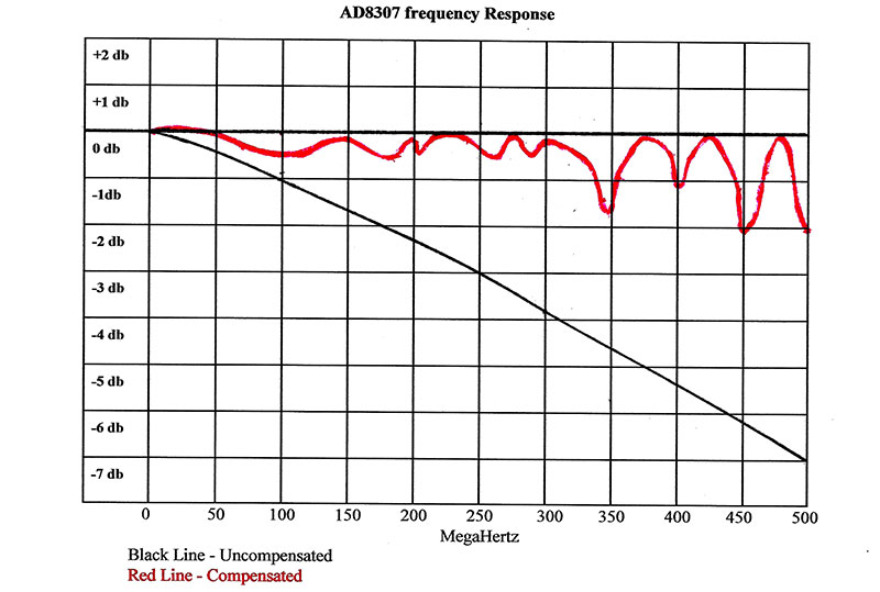
FIGURE 1.
As you can see, the response is quite accurate up to about 330 MHz at ± 0.5 dB, and then starts to get more erratic as it enters the UHF region (with errors up to 0-2 dB). This is pretty much what I expected for this method of compensation. Actually, a 2 dB error is not all that bad for general use power detection.
What I tried to do here is optimize the VHF band at the expense of the UHF band; reason being is that I am most comfortable and do most of my work in that range. As for UHF, I occasionally do some work in the ISM and FRS radio services, and the aforementioned trade-off has caused me no major problems.
The compensated attenuator method of compensation would probably have given me a more uniform roll-off, but much poorer overall response across these spectrums. Plus, it would still cause some amount of reflected energy at various points. Unfortunately, optimum designs are usually a series of trade-offs.
Since the temperature adjust and offset pins (pin 3, pin 5) are of little consequence in this application, they can just be left floating. That only leaves the output pin (pin 4) to deal with. As mentioned, this outputs 25 mV per dBm of input. This will have to be scaled to match whatever read-out is used. In this case, it will be a digital voltmeter.
To save some money, you could use a standard DMM by bringing these metering points out to a pair of pin jacks on the rear of the case to accept the DMM probes. One objective I wanted to accomplish was to keep the circuit as simple as possible and without any additional active components aimed at keeping the current requirements very low to prolong battery life. Other than a five volt regulator, it only needs two multi-turn trim pots and a few resistors. In this configuration, it only requires about 10 mA for operation.
At this point, we’ll take a quick run-through of the circuit as shown in Figure 2.
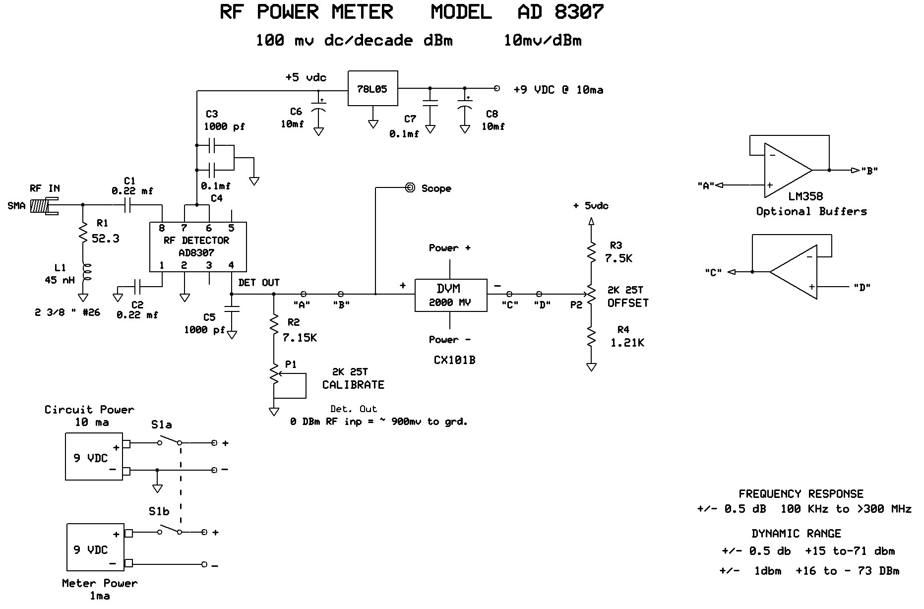
FIGURE 2.
The RF test signal enters SMA connector J1 which is terminated by the series arrangement of R1, L1. From there, it is coupled via C1 to IC1 pin 8 (RF Input Hi). Pin 1 (RF input Lo) is decoupled to ground via C2. The +5 VDC supply feeds P6, P7 and is decoupled via C3, C4. The detector DC output (pin 4) drives the positive terminal of the digital voltmeter. During the calibration procedure, this will be adjusted for 100 mV per decade of dBm input.
The pins internal circuitry uses a constant current source of 2 µA per dBm of RF input to output a DC level here. The nice feature of a CC source is you can easily choose the values of P1, R2 for any desired DC level at that point. And again, it will be set for 100 mV/dBm decade.
The term 0 dBm actually has a valid power level and denotes a reference power level of one milliwatt dissipated in a given load.
C5 is chosen for ripple reduction of the detected DC output. I chose 1,000 pF as it adequately tamed the ripple yet still maintained a short enough time constant for good fidelity of sweep testing amplifiers and filters with very steep roll-offs. The offset circuitry P2, R3, R4 completes the circuitry and is there for only one purpose: to trick the meter into reading the digits we want to see and not the actual detector output DC. (More on this in the calibration procedure.)
The only other thing to mention here is the use of two 9V batteries. My first designs used a single battery for both the circuit and meter. This required that the meter power and inputs share a common ground and measure all voltages relative to that point. Due to the meter “tricking,” the circuitry would now require some op-amps and also a split supply to accomplish that.
The negative voltage needed was done quite simply with a 7660 inverter chip, and it was very efficient in its operation. However, this chip really made a racket and caused switching spikes everywhere that I could not totally eliminate. Even though they were present at the meter’s input, they were too fast to cause anything but minimal errors that most of the time went unnoticed. When using the optional scope output jack, however, they were a nuisance — especially when increasing the vertical sensitivity. I lived with that design for a while and then decided to ditch it.
The new version with an extra dedicated meter battery really does not hog up much real estate and with the meter only drawing 1 mA, it should last “forever.” Also, I use 50 cent batteries from a local dollar store for the meter, so the extra cost is of not much consideration.
One last word here. If desired, points “A-B” and “C-D” can be opened and an LM358 optional buffer inserted in those spaces. This makes sending the detector’s output to the outside world (such as a scope, etc.) a lot easier and offers a slight improvement in accuracy and ease of calibration. This will only add 1 mA of extra battery load current so as to be insignificant. I decided that this was the best route to take.
Construction of the circuit board is very simple. The beauty of it is that only the first inch of it deals with radio frequency. However, I would recommend a ground plane using a single-sided board for the complete circuit. I cut a 1” x 2-1/4” board for this which was mounted to the box with two 3/8” long metal standoffs to the end opposite the SMA connector.
The circuit components are a combination of surface-mount and thru hole construction. All thru hole components were mounted on the glass side of the board and SMD devices were used only for the RF input section as shown in Figure 3 and Figure 4. Keep traces short and components close in this section.
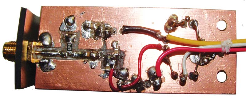
FIGURE 3.
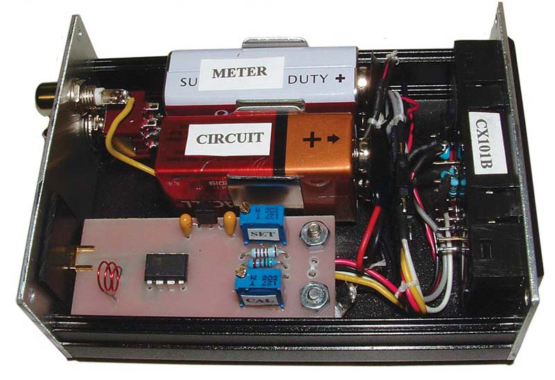
FIGURE 4.
The SMA connector should be as close as possible to the 8307 chip. The SMA to chip input trace shown in Figure 3 was longer than necessary to accommodate any changes that I may have wanted to make here. No changes were needed, and that trace could have been shorter. The coil L1 is a length of 2-3/8” #26 wire and loosely wound in a few turns to better fit in its designated space. If you use a more common 24-gauge wire, allow a little extra length of a 1/4” or so. The winding pitch and coil dimensions are not critical here, but the key word is “loose.”
You may notice a bracket shoved up tight to the SMA base. This was to offer support on that end of the board because the only circuit board standoffs used are at the opposite end of the board. This can be cut from a dielectric material (I used wood) approximately 1/8” thick and cut to length so as to tightly capture the SMA in place when the cover(s) are installed, keeping the SMA very ridged so it can stand up to many cable connections/disconnections.
As shown in Figure 5, the back panel entry hole was cut larger than needed to allow more positive clearance for the SMA connector and to give ohmic clearance to the cable connector shell to chassis ground to better simulate a full 50Ω environment right from the DUT (Device Under Test) to the board’s launching point.
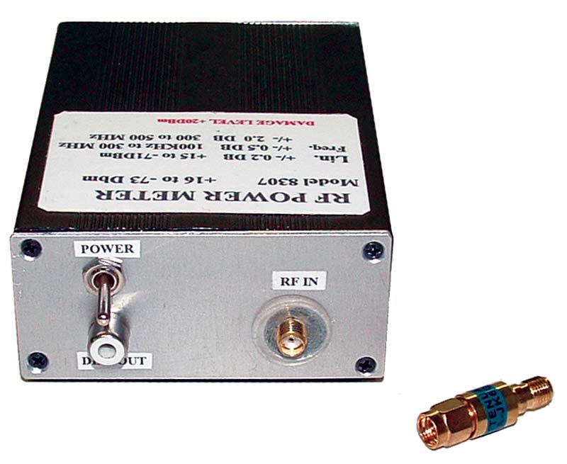
FIGURE 5.
A DPDT power switch and scope out phono jack complete the hardware used here. Four leads were brought off the board to a small four-pin connector which then branch out to the battery (two) and the meter (two). The batteries were installed in vertical snap clips.
Now for a word about meter requirements. The digital readout should have the following requirements:
- 200.0 mV max sensitivity range
- 10 megohms of input impedance
- Ability to display a two-volt range
- Selectable decimal point location
- Leading zero suppression
- Independent operation from nine volt battery
- Very low current draw; usually requires LCD readout
- Polarity sign (does not need to show positive polarity)
That last requirement is very important as some readings would be ambiguous without it. Example: A meter reading displays 10 but what is it? +10 dBM or -10 dBm? No way to tell without a polarity sign!
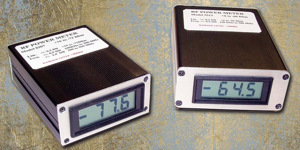
Although there are many meters available, the meter I used was a CX101A which fulfills all the above requirements. Plus, I’ve used these in the past with very good results. The meter snaps into a close tolerance panel cut-out. Again, I used a miniature four-pin connector to its flying leads. These also branched out to its own battery (two) and the circuit board connector (two).
All the assemblies fit snugly in an extruded aluminum housing with removable covers, and it measures approximately 4” L x 3” W x 1-1/2” H. It was purchased on eBay (they’ve been quite plentiful for a while now). As I said, it’s a snug fit which requires some fairly accurate machining. So, if you’re not quite up to speed on these skills, you may want your housing to be a bit larger.
As mentioned previously, construction of the AD5513 version is almost identical to the AD8307 model. Figure 6 shows its schematic.
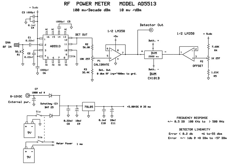
FIGURE 6.
The major difference here is that L1 is not needed and this chip is only available in an SMD style which is a small 16-pin PLCC package. Although it has 16 pins, it only needs eight islands as the pins marked ‘NC’ can be either soldered to the ground plane or left floating.
One point must be made perfectly clear: dB and dBm are two different terms and each should be used in its proper place.
This chip is a current hog and the circuit draws 35 mA. With that in mind, I added an external power jack for times when it sees extended bench use. You’ll want a bigger board for the AD5513 model or if you add the optional buffers on the AD8307 model, and, of course, the housing that they fit in.
Either of these chips cost about $11-$12 and are available through Mouser and Digi-Key, but they do appear on China eBay in an evaluation board style averaging $15 for the AD8307 and $27 for the AD5513.
The trim pots are 25-turn, but 10-turn would be acceptable. All capacitors (except the few 10 MFD ‘lytics ) are MLC ceramics/50V and all resistors are 1% metal film. Since the calibration resistors are in a string with trimmer pots, you can get by with 1% resistors that are close in value to the ones shown on the print or even 5% carbon film of the nearest values. However, R1 should be kept at 1% metal film and at least a 0.25 watt rating (or better yet, 0.5 watt). The metal film versions have superior RF performance as compared to carbon film. The op-amp chips can be socket installed if used, but the AD8307 and/or AD5513 should be soldered directly to the board for the best RF performance.
Calibration and Use
Once the circuit board is completed, give it a close inspection before applying power to it. The AD chips are fairly expensive, so you want to be doubly sure about power connections and polarity. After power-up, connect a DMM from the positive terminal of the internal voltmeter to ground. Inject an RF signal of 0 dBm into the SMA input. (I’ll discuss the signal issue in a while, but for now, I’ll just continue with the calibration.)
For starters, set the CALIBRATION pot for a DMM reading of approximately 900 mV DC. Next, you’ll need a way to attenuate the input signal in 10 dB steps of at least four steps (more steps are better). You’ll need to adjust the pot for very close to 100 mV of change for every step of attenuation. This will involve some back and forth adjustments but try to get as close to the 100 mV steps through all the attenuated levels you are measuring.
Again, four steps down to -40 dBm is adequate but if you have the means to go further, then do so. You should end up with no more error than 1 or 2 mV per step of the target value. Don’t worry about where the 0 dB value ends up; only that it tracks the other steps. It will probably end up somewhere in the 880 to 920 mV range (referenced to ground); not important.
When you’re satisfied with your results and with the input signal set at 0 dBm, adjust the OFFSET pot so that the internal meter reads exactly zero. This completes the calibration procedure and depending on the AD chip used, it should be quite accurate all the way to the bottom of its linear range (deeper than -70 dBm for the AD8307 and -55 dBm for the AD5513).
When measuring signal levels below that, at first the reading will begin to deteriorate a little and then more rapidly as it approaches the noise floor. You can expect about 5 dB lower than the linear portion just before it hits the noise floor. The noise floor is the reading you get with no signal inputted and the meter is just reading its own internally generated noise at that point. Any input signal below this level will hardly even register on the meter.
Now some words about accuracy and test signals. Any piece of test equipment can only be as accurate as the standard it is calibrated to. My “standard” for calibrating these meters is an HP RF generator from the ‘80s. Most of the generators from that era had incredibly accurate attenuators and superior flatness across their range. In all the years of checking and cross-checking across its range against new product specs and other quality test equipment, it has always proved trustworthy. Other owners of that gear have also echoed my sentiments, saying that it was about as accurate as one could read the meter.
dB has no value at all and only indicates a mathematical ratio. dBm has an absolute value and is not a mathematical term per se.
With that said, I used an output range of +20 dBm to -80 dBm at a frequency of 10 MHz for calibration in regards to dynamic range and an output of 0 dBm for checking wide band frequency response. I also made up a ‘standard’ test cable using quality RG-58 cable and with quality type N to BNC connectors. It’s 36” long and easily reaches between any gear on the bench or from bench to cart.
This eliminates at least one variable for future tests and calibration checks.
Again, and before I get into possible signal sources, I would like to categorize power meter accuracy vs. performance level. This is the order in which I would rate them:
- ± 3 dB: JUST BARELY ADEQUATE for non-critical testing. These specs are still used in equipment such as oscilloscope bandwidth, various amplifiers, etc.
- ± 1 dB: GOOD. Accurate enough for a majority of testing.
- ± 0.5 dB: VERY GOOD. Adequate for almost any testing.
- ± 0.1 dB: EXCELLENT. Adequate for any testing and more confidence in the results.
- << ± 0.1 dB: COMMERCIAL LAB TESTING. Well beyond what most would ever need.
For the two meters I’ve described in this article, I would rate the AD8307 meter in the good range and the AD 5513 meter in the good to excellent range. With lab quality meters that are at and beyond the excellent range, there is one caveat: maintaining a near perfect match between the source and the load (which is the meter in this case). The setup requires high quality cable and connectors for starters, and in a lot of situations, special test jigs which require more and more construction precision as the frequency enters the lower UHF band and upwards.
Most of the time, the term dB is used to spec out parameters such as gain, loss, etc.; dBm, on the other hand, is used mostly for results as to absolute power levels.
To make use of these instrument’s very high accuracy, all setup errors must be eliminated. Not an easy task if you’re attempting to measure a low level signal of 2 GHz at 0.03 dB resolution. Without a lot of care in these regards, one will have lost a lot of accuracy and paid a lot of money for readings that are far from highly accurate. Fortunately, for the average user that the meters presented here are intended for, we don’t have to go to those extremes — especially at the lower frequencies.
Now back to signal sources used for calibration. Obviously, you want to use the best signal source you own, or can “beg, borrow, or steal” for this task. This can end up being anything from a top-of-the-line RF signal generator down to a low grade function generator. The higher quality the source, the easier the calibration will be (such as a flat signal amplitude output and a quality built-in attenuator). There is one saving grace here and that is you can use a test signal as low as 1 MHz since it’s well within the pass band of either of the two meters. At these frequencies, almost any “service grade” function generator and scope will work okay.
No matter what you use, the sine wave input levels you’ll be concerned with are: 0 dBm /632 mV P-P; -10 dBm /200 mV P-P; -20 dBm /63 mV P-P; -30 dBm /20 mV P-P; and -40 dBm /6.3 mV P-P. The negative 30 and 40 dBm levels are rather low, but the scope can use an X1 probe to measure all of these levels — even right at the meter’s input connector.
At 1 MHz, mismatching and probe capacitance will not be much of a problem. You can adjust the different levels as you go through the calibration procedure (which tends to get annoying) or you can build up a 50Ω Pi attenuator network on a solderless breadboard with stub-outs for each level point. An upgrade to this would be to tack in a rotary switch in place of the stub-outs.
One last thing to mention here: While perusing all the AD datasheets early in my research, there was a detailed explanation in one of them that pertained to how these RF log detectors work. Most of it was a lot of high-tech theory, but what really caught my eye was the part that mentioned their response to square waves.
It was shown that a square wave of exactly half of the peak-peak value of a sine wave would give the same DC voltage output from these chips. Doing a little math on this, I actually came up with levels that were -3 dB lower for the square wave vs. sine wave. I was a little skeptical that this would work, so I fired up my function generator and set it up for a 1 MHz sine wave 0 dBm output (632 mV P-P) which read 0.0 dBm on the RF power meter.
Next, I switched to a square wave of exactly half of that amplitude (316 mV P-P) and was pleasantly surprised to see a 0.0 dBm readout on the meter. Apparently, the way these chips analyze the input waveform has to do with peak values and cresting factors that give those results on square waves (remember, I had previously mentioned that these chips rely on a reasonable facsimile of a sine wave for accurate measurements). I still had faith in my math and am sure that a high-priced power meter using thermal sensing rather than voltage would give the lower reading.
With that kept in mind, these meters work well using square waves and they can also be used for calibrating. My function generator has a 50Ω output impedance, 10:1 variable attenuator, and two switched 20 dB attenuators. Surprisingly, the two switched attenuators gave very accurate results. I tried to go deeper than that with an external wide band attenuator, but results I got below -40 dB were losing accuracy. I’m not sure why. I think with a little development work, this problem could be remedied, and a descent calibrator could be built up, but I did not pursue it any farther.
I think that most RF engineers would agree that accurate measurement of RF power levels is one of the more difficult measurements to achieve, and they’ll get no argument here.
The two chips used in this article are quite amazing in their performance. They’re very stable and repeatable, and will rival accuracies of commercial power meters in your lab that you could only dream of owning several years ago.
Of the two meters shown here, the big question is which one to build. The AD8307 has a tremendous dynamic range of about 85 dBm, while the AD5513 has superior accuracy and excellent performance over a wide band of frequencies. My limit for testing the latter one was 520 MHz, but the datasheets show good performance beyond 3.5 GHz. Since I couldn’t pick one over the other, I ended up building both of them.
One last item to mention here is the small golden object shown in Figure 5. This is a 20 dB attenuator which can be inserted between the meter and test cable. I bought this on eBay for $7. This adds 20 dB more to the high-end range of measurement to these meters; the AD8307 model now has a dynamic range of 105 dBm, which is a power range of >2 watts (~ 10V RMS) down to < 0.1 nano watt (~70 uV RMS). Pretty impressive!
Conclusion
A few last words to close out this article. Due to the excess length of magazine space this subject would require and in order to discuss additional ancillary circuits, etc., I have info packets available by email. This would cover some auxiliary circuits such as calibrators, scope interfaces, etc., including an interface circuit that is especially useful for setting up the scopes vertical attenuator to match any dB value per graticule you would desire. Thus, sweep testing would give perfect sweep displays of flatness and roll-offs in calibrated dBs. NV
| PARTS LIST FOR AD5513 MODEL |
PARTS LIST FOR AD8307 MODEL |
| R1 |
52.3Ω 1/4W or 1/2W (preferred) |
R1 |
52.3Ω 1/4W or 1/2W (preferred) |
| R2 |
56.0K Ω 1/4W |
R2 |
7.15K Ω 1/4W |
| R3 |
32.4K Ω 1/4W |
R3 |
7.5K Ω 1/4W |
| R4 |
7.68K Ω 1/4W |
R4 |
1.21K Ω 1/4W |
| R5 |
1.21K Ω 1/4W |
|
|
| C1, C2, C8 |
0.22 MFD 50V MLC |
C1, C2 |
0.22 / 50V MLC |
| C3, C5, C6 |
0.001 MFD 50V MLC |
C3, C5 |
0.001 / 50V MLC |
| C7 |
1000 MFD 16V Electrolytic |
C4, C7 |
0.1 / 50V MLC |
| C4, C10 |
0.1 MFD 50V MLC |
C6, C8 |
10 MFD / 16V electrolytic |
| C9, C11 |
10 MFD 16V Electrolytic |
|
| |
|
L |
45 nH (see text) |
| P1 |
10K Ω 10T or 25T |
|
| P2 |
1K Ω 10T or 25T |
P1, P2 |
2K Ω 10T or 25T |
| IC |
RF Detector |
AD5513 |
IC |
RF Detector |
AD8307 |
| IC |
Buffers |
LM358 |
IC |
Optional Buffer |
LM358 |
| IC |
Regulator |
78L05 |
IC |
Regulator |
78L05 |
| Schottky diodes |
BAT25 |
|
DVM |
CX101B |
|
| DVM |
CX101B |
|
|
Downloads
What’s in the zip?
Application Note
dB or not dB? Everything you ever wanted to know about decibels but were afraid to ask…
courtesy Rohde & Schwarz