Part 1 gave you an overview of logic analyzer basics. Now, let’s concentrate on actually using this instrument. We’ll examine some of its limitations and its numerous, powerful features that make it so useful in the lab, production line, academic and research environments, as well as in development and maintenance applications.
Acquisition of Simultaneous State and Timing
During hardware and software debug (system integration), it’s helpful to have correlated state and timing information. You may initially detect a problem as an invalid state on the bus. Setup and hold timing violations may cause this. If the logic analyzer cannot capture both timing and state data simultaneously, isolating the problem becomes difficult and time-consuming. Some logic analyzers require connecting a separate timing probe to acquire the timing information and use separate acquisition hardware.
These instruments require you to connect two types of probes to the SUT (system under test) at once (see Figure 1).
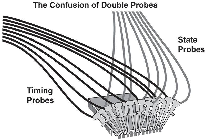
FIGURE 1. An illustration of how double probing requires two separate probes on each test point, which decreases the quality of the measured parameters sought.
One probe connects the SUT to a timing module, while a second probe connects the same test points to a state module. This “double probing” arrangement can compromise your signal’s impedance environment. Two probes will load down the signal, degrading the SUT’s rise and fall times, amplitude, and noise performance. Figure 1 is a simplified illustration showing only a few representative connections. In an actual measurement, there might be four, eight, or more multi-conductor cables attached.
The Confusion of Double Probing
It is best to acquire timing and state data simultaneously through the same probe at the same time (see Figure 2).
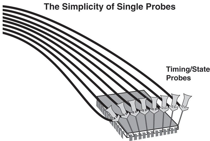
FIGURE 2. An illustration of how simultaneous probing provides state and timing acquisition through the same probe, which is a much “cleaner” measurement environment.
One connection, one setup, and one acquisition provide both timing and state data. This simplified mechanical connection reduces problems. Simultaneous timing and state acquisition allows your logic analyzer to capture all needed information to support both timing and state analysis.
There is less chance of errors and mechanical damage that can occur with double probing. The single probe’s effect on the circuit is lower, ensuring more accurate measurements and less impact on your circuit’s operation. The higher the timing resolution, the more details you can see and trigger on in your design. This increases your chance of finding problems.
Real-time Acquisition Memory
The logic analyzer’s probing, triggering, and clocking systems deliver data to the real-time acquisition memory — the heart of the instrument. This is the destination for all of the sampled data from the SUT and the source for all of the instrument’s analysis and display.
The logic analyzer memory stores data at the instrument’s sample rate. Think of this as a matrix having channel width and memory depth (see Figure 3).
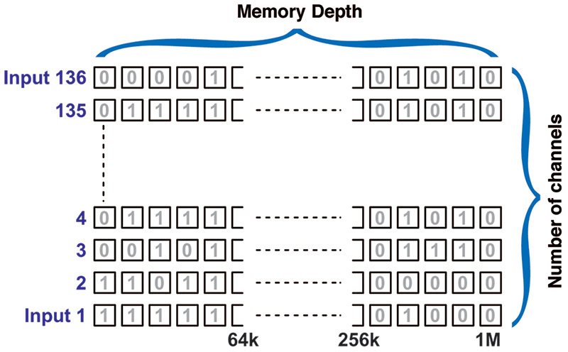
FIGURE 3. An illustration of how a logic analyzer can store acquisition data in a deep memory with one full-depth channel supporting each digital input.
The instrument accumulates a record of all signal activity until a trigger event or the user tells it to stop. The result is an acquisition — essentially a multi-channel waveform display that lets you view the interaction of all the signals you’ve acquired, with very precise timing.
For a given memory capacity, the total acquisition time decreases as the sample rate increases. For example, the stored data in a 1M memory spans one second of time when your sample rate is 1 µs. The same 1M memory spans only 10 ms of time for an acquisition clock period of 10 ns. Acquiring more samples (time) increases your chance of capturing both an error, and the fault that caused the error (see Figure 2 again). This illustrates how simultaneous probing provides state and timing acquisition through the same probe, for a simpler, cleaner measurement environment.
Logic analyzers continuously sample data, filling up the real-time acquisition memory, and discarding the overflow on a first-in, first-out basis, as shown in Figure 4.
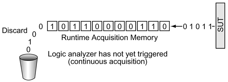
FIGURE 4. An illustration of how a logic analyzer can capture and then discard data on a first-in, first-out (FIFO) basis until a trigger event occurs.
Thus, there is a constant flow of real-time data through the memory. When the trigger event occurs, the “halt” process begins, preserving the data in the memory.
The placement of the trigger in the memory is flexible, allowing you to capture and examine events that occurred before, after, and around the trigger event. This is a valuable troubleshooting feature. If you trigger on a symptom — usually an error of some kind — you can set up the logic analyzer to store data preceding the trigger (pre-trigger data) and capture the fault that caused the symptom. You can also set the logic analyzer to store a certain amount of data after the trigger (post-trigger data) to see what subsequent effects the error might have had.
Other combinations of trigger placement are available (see Figures 5 and 6). With probing, clocking, and triggering set up, the logic analyzer is ready to run. The result will be a real-time acquisition memory full of data that can be used to analyze the behavior of your SUT in several different ways.
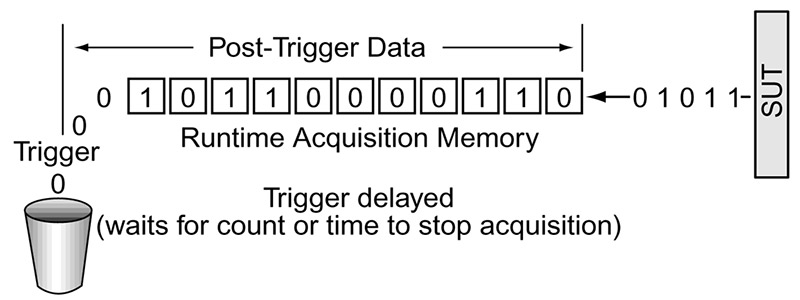
FIGURE 5. An illustration of how a logic analyzer can capture data that occurs a specific number of cycles later than the trigger.
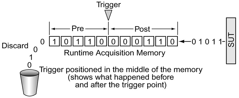
FIGURE 6. An illustration of how a logic analyzer can capture data around the trigger. Data to the left of the trigger point is “pre-trigger” data, while data to the right is “post-trigger” data. You can position the trigger from 0% to 100% of memory.
Analysis and Display
The data stored in the real-time acquisition memory can be used in a variety of display and analysis modes. Once the information is stored within the system, it can be viewed in formats ranging from timing waveforms to instruction mnemonics correlated to source code.
Waveform Display
The waveform display is a multi-channel detailed view that lets you see the time relationship of all the captured signals, much like the display of an oscilloscope. Figure 7 is a simplified waveform display. In this illustration, sample clock marks have been added to show the points at which samples were taken.
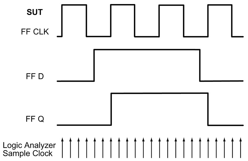
FIGURE 7. An illustration of a logic analyzer’s display, (somewhat simplified) so it remains uncluttered for discussion purposes.
You commonly use the waveform display in timing analysis, and it is ideal for:
- Diagnosing timing problems in SUT hardware
- Verifying correct hardware operation by comparing the recorded results with simulator output or data sheet timing diagrams
- Measuring hardware timing-related characteristics: - Race conditions - Propagation delays - Absence or presence of pulses
- Analyzing glitches Integrated Analog-digital Display
Older digital systems could tolerate wide variances of digital signals. In newer systems with faster clock edges and data rates, this is no longer the case. As design margins decrease, analog characteristics of digital signals increasingly affect the integrity of your digital system. A time-correlated analog-digital display using a logic analyzer with an oscilloscope gives you the ability to see the analog characteristics of digital signals in relation to complex digital events in the circuit, so you can more easily find the source of anomalies (see Figure 8.)

FIGURE 8. A time-correlated analog/digital view of an anomaly.
The listing display provides state information in user-selectable alphanumeric form. The data values in the listing are developed from samples captured from an entire bus and can be represented in hexadecimal or other formats. Imagine taking a vertical “slice” through all the waveforms on a bus (see Figure 9). The slice through the four-bit bus represents a sample that is stored in the real-time acquisition memory. Figure 9 shows the numbers in the shaded slice are what the logic analyzer would display, typically in hexadecimal form.
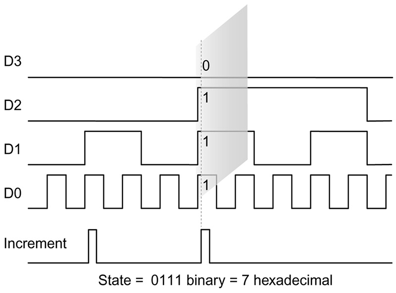
FIGURE 9. An illustration of how a logic analyzer’s state acquisition captures a “slice” of data across a bus when the external clock signal enables an acquisition.
The intent of the listing display is to show the state of the SUT. The listing display in Figure 10 lets you see the information flow exactly as the SUT sees it as a stream of data words.
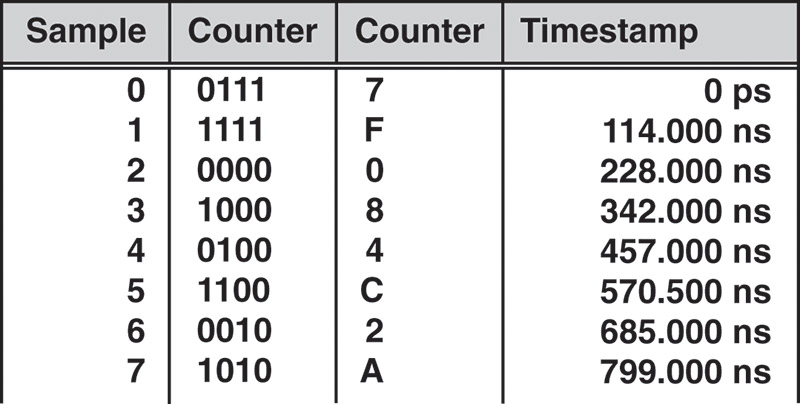
FIGURE 10. A display listing.
State data is displayed in several formats. The real-time instruction trace disassembles every bus transaction and determines exactly which instructions were read across the bus. It places the appropriate instruction mnemonic, along with its associated address, on the logic analyzer display.
Figure 11 is an example of a real-time instruction trace display. An additional display — the source code debug display — makes your debug work more efficient by correlating the source code to the instruction trace history.
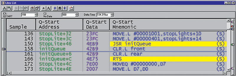
FIGURE 11. A real-time instruction trace display.
It provides instant visibility of what’s actually going on when an instruction executes. Figure 12 is a source code display correlated to the Figure 11 real-time instruction trace.
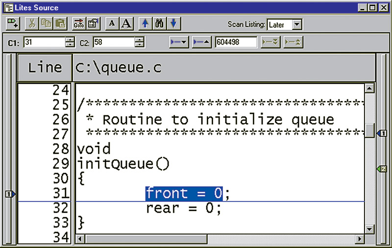
FIGURE 12. Source code display. Note that line 31 correlates to sample 158 in the instruction trace display in Figure 9.
With the aid of processor-specific support packages, you can display state analysis data in mnemonic form. This makes it easier to debug software problems in the SUT. Armed with this knowledge, you can go to a lower-level state display (such as a hexadecimal display) or to a timing diagram display to track down the error’s origin.
State analysis applications include:
- Parametric and margin analysis (e.g., setup and hold values).
- Detect setup and hold timing violations.
- Hardware/software integration and debug.
- State machine system optimization: line 31 in Figure 12 is correlated with sample 158 in the instruction trace display of Figure 9.
- Capture and analyze real-time system operation in order to debug, verify, optimize, and validate the design.
This trend — the virtual substitution of the logic analyzer for the traditional microprocessor emulation tool (in-circuit emulator or ICE) — continues today. The result, therefore, is that those who need the principal function of a logic analyzer — the selective acquisition of digital data and its display as a pattern of waveforms — have a tool that has a different emphasis and high cost.
Monitoring microprocessor CPUs is easier with states translated into assembly code, so this type of capability was available as a logic analyzer option for each common µP IC family. However, integrated hardware and software control was not generally possible with logic analyzers. This labor-intensive process usually involved writing the software, then compiling/assembling it, translating it into a downloadable format, and then downloading it into the system. The logic analyzer then monitored the new software version.
An In-Circuit Emulator
This is a collection of hardware and software. The hardware consists of a host computer system (typically significantly more powerful than the CPU of the system being emulated) and an interface to the target processor’s socket. The interface consists of logic and a cable which plugs into the socket intended for the target processor. The hardware and software work together to allow the target system to debug it under your control. The cable takes the place of the microprocessor IC, or connects to the µP IC and disables the µP IC to allow host system control.
Newer systems allow the same sort of debug capability with a simpler hardware interface. Debug and test hardware is built into a microcontroller, which is a microprocessor-based system on a chip. The system includes many standard peripherals such as serial interfaces, parallel interfaces, timers, priority interrupt controllers, clock management circuits, a simple high-speed serial interface, possibly USB port hardware, and — most importantly — a four-wire test interface that IEEE 1149 specifies and Joint Test Architecture Group (also known as JTAG) manages.
This JTAG interface came into existence to support the boundary scan test of ICs, but is so versatile you can use it to populate nonvolatile system memory and program logic devices such as CPLDs in place. The JTAG is a serial bus which you can daisy chain that allows you to test and/or program many devices.
System designers program PALs, PLAs, and more recently CPLDs. The configuration is unknown until you decide the programming, so the manufacturer cannot completely test the parts. Unless you select pins for test points, making them generally unavailable for functional use.
There is no internal circuit access for use with a logic analyzer. Therefore, programmable logic support software must include a simulator to allow you to conceptually test the simpler designs and ultimately generate test vectors to verify the correct programming of these parts. The device programmer uses the test vectors for simpler devices, such as PALs and PLAs.
Use of the JTAG port on newer, more complex devices allows testing of the devices you have programmed and placed in the circuit. JTAG-equipped devices require only a four-pin penalty to support this flexibility.
You can use simpler logic analyzers to test the remaining circuits on a system with microcontrollers and dense programmable parts like CPLDs. Cards which you can implement as a PC peripheral board need to only have simple state measurement and trigger capabilities which you can control and expand by the PC. Logic analyzers are therefore useful for tracing down glitches in the “glue” logic. NV
Acknowledgements
I wish to thank Matt Litfin of Tektronix for both supplying artwork, as well as reading the finished manuscript, ensuring its technical accuracy, and John Stabler, my boss, for information related to in-circuit emulators and the JTAG.