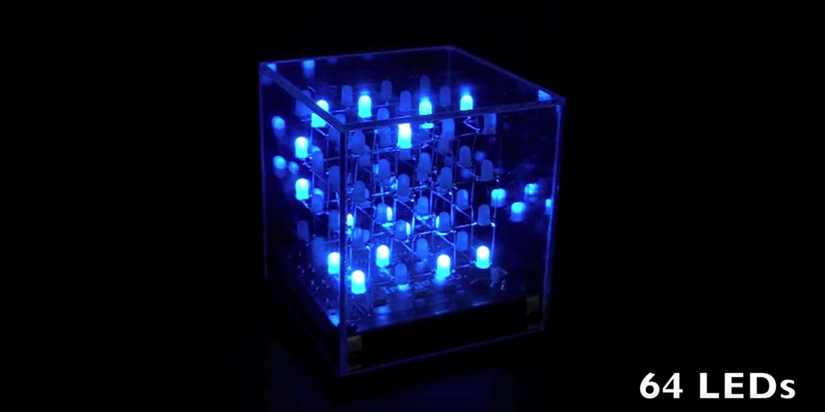
This article shows you how to build a really cool 3D cube with a 4 x 4 x 4 monochromatic LED matrix which has a total of 64 LEDs. This size provides the best value for construction time and programming time for 3D patterns. The advantage to using monochromatic LEDs is that they are very bright, so are therefore easy to see — even in a well lit room. Many RGB LEDs don’t have the same light intensity punch and when used in the 3D LED cube, can only be viewed in a dark room.
Check out the video!
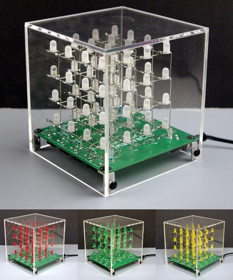
You have a choice of four monochromatic colors: blue, red, green, and yellow (Figure 1).
FIGURE 1. The 3D LED Cube.
There is a kit for this project available from our webstore that includes a microcontroller with 29 pre-programmed patterns that automatically play. Runtime for all 29 patterns is approximately 6-1/2 minutes. Of course, you can also source the parts yourself from the parts list at the end and instructions on how to program the 3D matrix yourself are provided here also.
We will need the following tools for building both the LED cube and jig:
Soldering iron and solder.
Needlenose pliers.
Diagonal (lead) cutters.
20 gauge solid wire; one meter in length.
One 2AAA battery holder.
Two AAA batteries.
1K 1/4 watt resistor.
LED Cube Construction
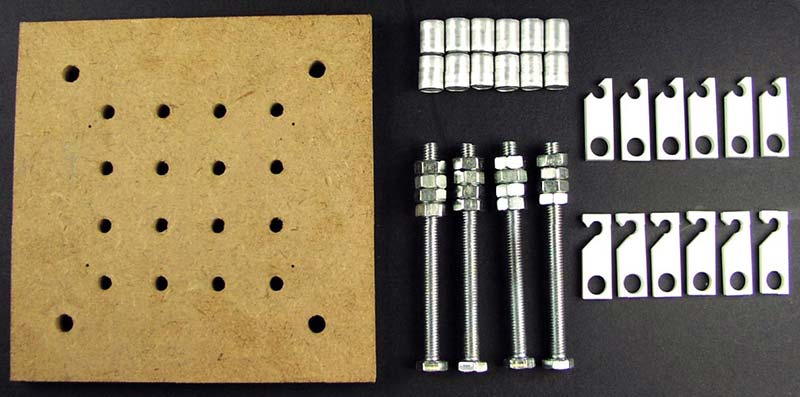
To accurately build the LED cube matrix so that everything is evenly spaced and aligned, I recommend building the jig described here. Instructions for using a jig are provided in this article. If you do not wish to use a jig, you can fabricate the LED matrix in any manner you find convenient. The jig contains the following parts: wood base; four 1/4-20 bolts, four inches in length; 16 1/4-20 nuts; 12 LED holders (two styles); and 12 spacers. See Figure 2.
FIGURE 2. Jig kit including wood base, LED holders, spacers, nuts, and bolts.
Physical Layout
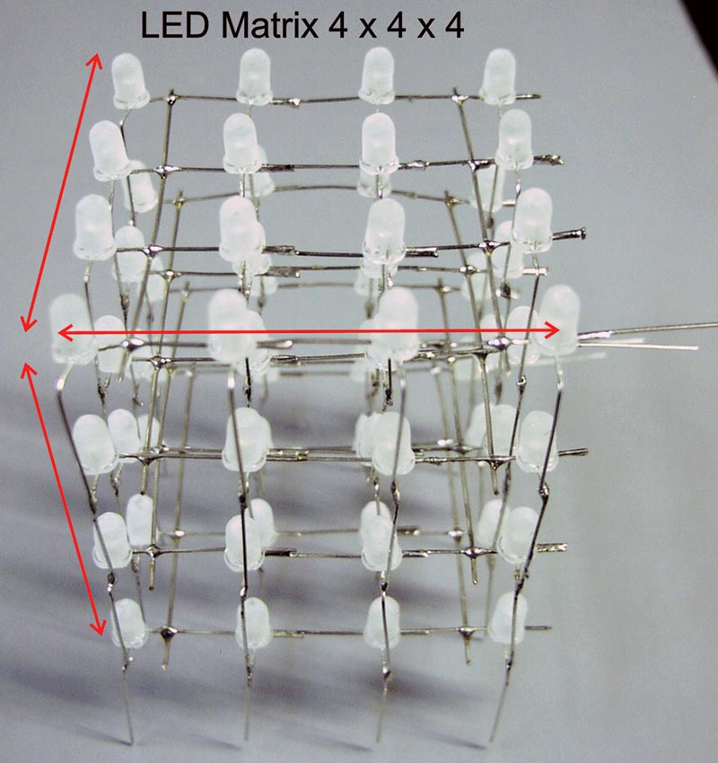
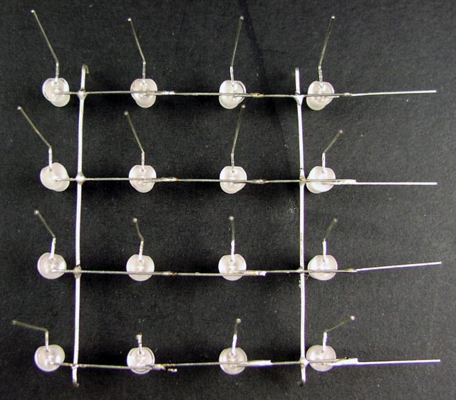
The LED cube has 64 LEDs in a 4 x 4 x 4 matrix (see Figure 3). There are four LEDs across the length, width, and height. Each of the four layers contain 16 LEDs. Physical dimensions are approximately 2.5” x 2.5” x 2.5”, with consecutive LEDs separated by 3/4”.
FIGURE 3. LED matrix 4 x 4 x 4.
LEDs
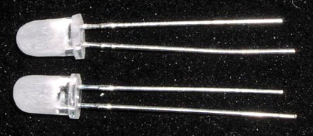
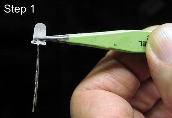
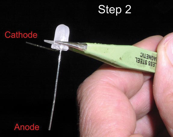
The LEDs are round and measure 5 mm (T1-3/4) (see Figure 4).
FIGURE 4. LED, showing lengths of cathode and anode leads.
Rectangular/oval shaped LEDs can be used, but may be a problem to hold during construction. A diffused lens will give you a wider viewing angle, especially for side viewing, so keep these things in mind if you’re purchasing your own LEDs. For the kit, we purchase super bright clear LEDs and sand blast them ourselvs to diffuse the lens. LED leads should be 1” long and are used to connect consecutive LEDs (which are 0.75 “ apart).
Electrical Connection
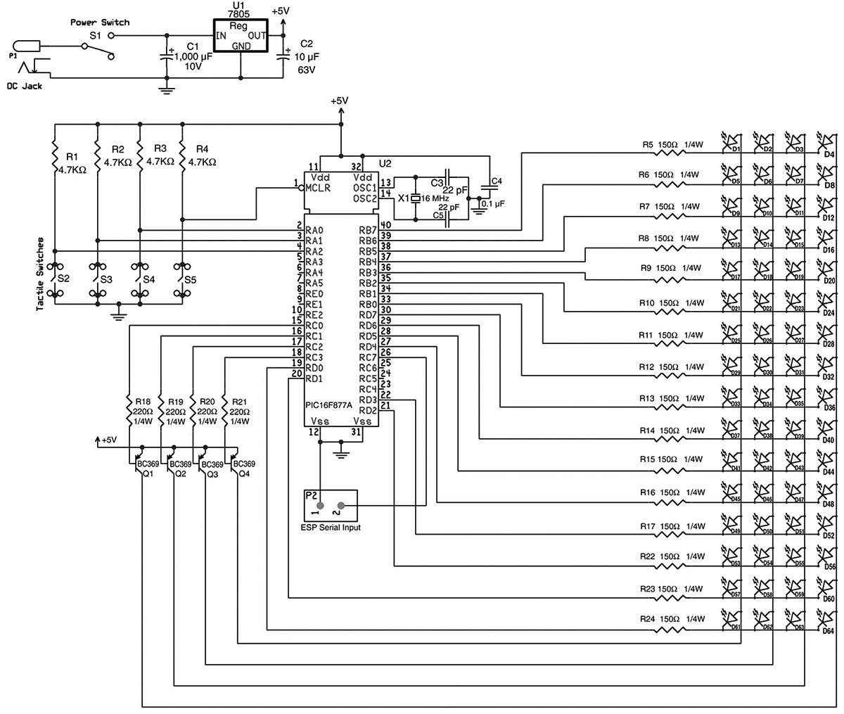
The schematic for the 3D LED cube is shown in Figure 5.
FIGURE 5. LED cube schematic.
The cube is a 16 x 4 multiplexed display, with 16 common cathode connections and four common anode connections. Each LED layer has 16 LEDs with one common anode. So, a total of four layers means four common anode connections. Each of four LEDs in a vertical line have a common cathode connection. So, 16 vertical lines means 16 common cathode connections.
Check Those LEDs
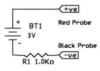
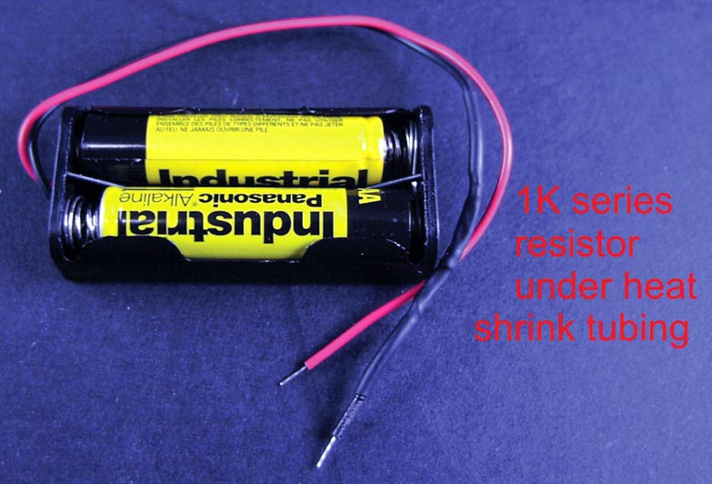
While the failure rate of new LEDs is extremely low, I recommend checking your LEDs before soldering them into the 3D matrix structure. It is very difficult to replace a faulty LED once the matrix is constructed. A simple LED tester can be made to help with this (see Figures 6 and 7). Take a two-battery AA or AAA battery holder and solder a 1K resistor in series with the black lead to limit current to the LEDs. This is shown as the –ve terminal; the red wire probe is the +ve terminal.
FIGURE 6. LED tester schematic.
FIGURE 7. LED tester.
Cube Jig
The layout for the jig is shown in Figure 8.
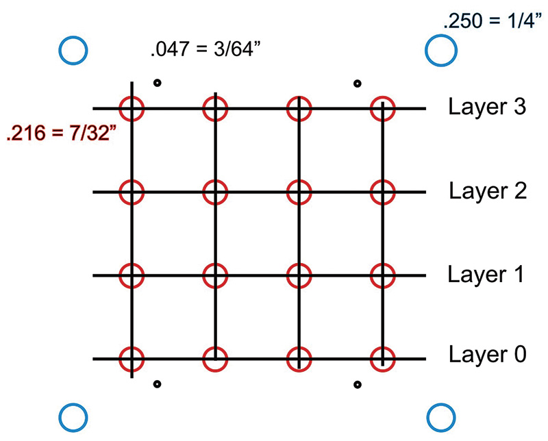
FIGURE 8. Drawing 6" x 6" jig wood base.
The jig itself is made from 6” x 6”, 3/8”-1/2” thick wood. The 16 holes with red numbers are 7/32” diameter, or a #7 drill bit. LEDs are inserted upside down into these holes. The four holes with black numbers are .047” in diameter; so that’s a 3/64” or #56 drill bit. These holes are used to hold thick tinned wires (about 0.8 mm wire without sleeve) in place.
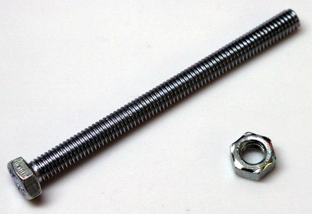
The four holes with blue numbers are 0.25” in diameter, or a 1/4” drill bit. Drill these holes to hold 1/4–20 bolts at the required positions. Be sure to label the jig with the diameters of the holes so that you can orientate it properly later. You’ll need to use spacers and nuts with the jig to achieve a height of 0.75” between the layers. If you don’t use a jig, your goal is to stack up three to four nuts to achieve a height of 2 cm (0.75”). The four 1/4” holes hold bolts (like the one in Figure 9) to which the LED holders attach to keep the layers one above the other at accurate positions. (This is actually not as complicated as it sounds; the photos should help.)
FIGURE 9. Close-up 4" bolt with nut.
Bolts are a minimum of 4” long. The 16 holes in the 4 x 4 grid are 13/64” in diameter (or a #7 drill bit). These holes will be used for making individual layers. Figure 10 shows the jig base.
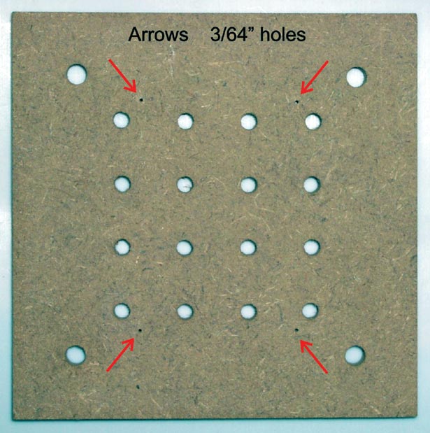
FIGURE 10. Wood base for jig, arrows to 3/64" holes for tinned wire.
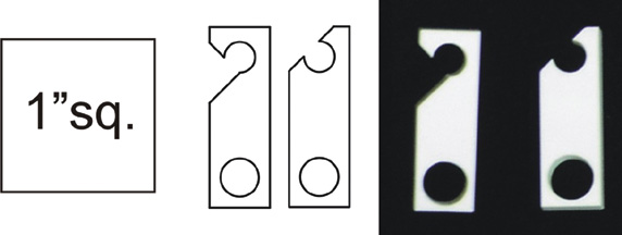
LED Layer Holders
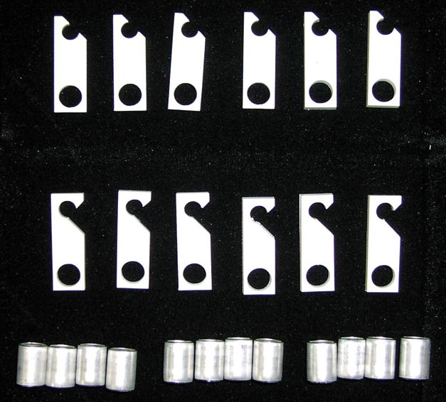
The holders are used to keep the layers at their required position above each other. We need a total of 12 holders, divided into two groups of six. Please note that both groups have minor differences (see Figure 11).
FIGURE 11. View of 12 LED holders and 12 spacers for jig.
Figure 12 shows the strip designs.
FIGURE 12. LED holders.
Use this layout in Figure 12 to make the strips. Glue the layout on 16 gauge sheet metal. Cut the sheet metal along the border lines with tin snips. Then, use a hole-punch to mark the centers where the cross lines intersect and drill the holes with the proper bits. The holes in the LED holders are 17/64” as opposed to 1/4” in the jig base. This slight increase in the hole allows for adjustments when positioning the LED layers. Holders are made from 1/8” acrylic.
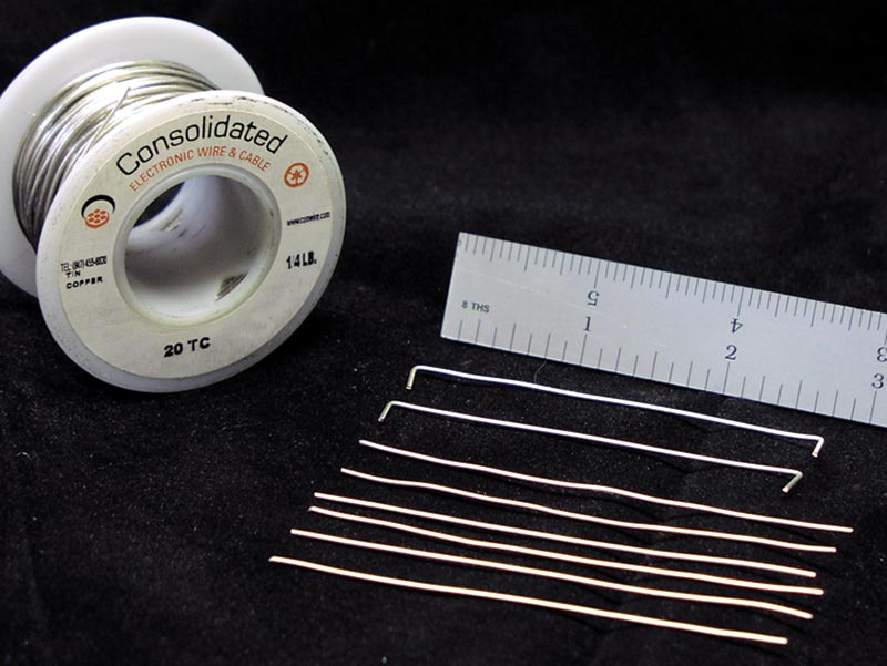
Tin Copper Wires
We will need two pieces of tin wire 3.25” in length per layer, for a total of eight wires for the entire LED cube construction (see Figure 13). If you are using wire from a reel, it should be straightened for proper and easy soldering. Try straightening the wires as much as possible by hand. Then, put the wires on a firm surface (e.g., desk) and use the jig base to roll over the wires, using some pressure. This will straighten the wires out perfectly.
FIGURE 13. Tinned wire, cut to length and formed for use on jig base.
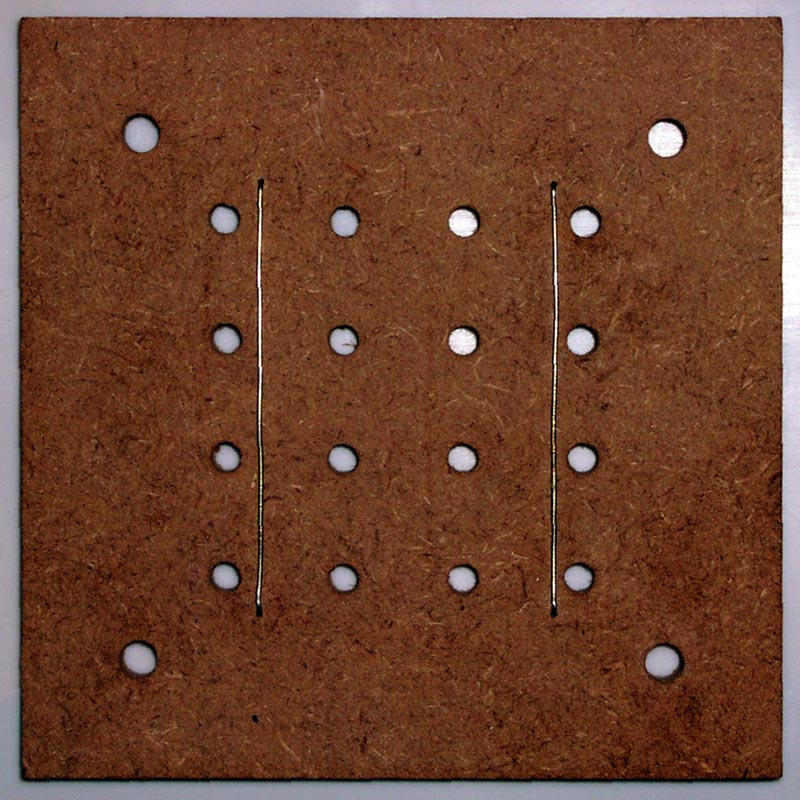
Tin Wire Forming
Orient the jig such that the 3/64” drill holes are at the top and bottom of the jig. Each of the eight tin wire pieces needs to be formed into a “C” shape for accurate and easy soldering. There are four small 3/64” holes drilled into the jig; with correct orientation, a pair of them will be in a vertical line perpendicular to you. Take a tin wire piece and make a 90 degree bend at 1/4” from one end. Insert the 1/4” bent portion into one of the 3/64” holes and align the wire with the corresponding 3/64” hole along a vertical line. Hold the wire over the second hole with needlenose pliers. Lift the bent end from the previous hole and make a 90 degree bend at the position where the pliers hold the wire. (This will give the C shape to the wire.) Repeat this process for the rest of the eight wire pieces. Figure 14 shows the jig with two tin wires preset into the 3/64” holes, ready to start accepting LEDs.
FIGURE 14. Jig base with two tinned wires loaded.
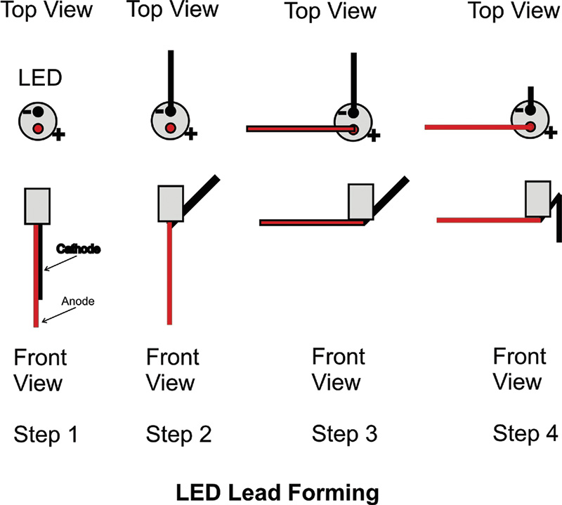
LED Leads Forming
We are going to use LED leads to help solder the LEDs into each layer. The most important step is bending the LED leads properly. Figure 15 provides an overview of the four steps.
FIGURE 15. Graphic showing 4 steps in LED formation for use in jig.
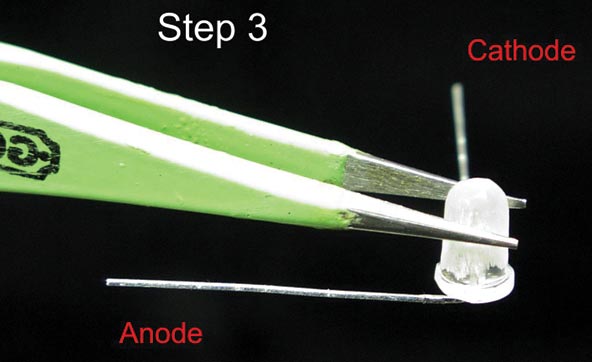
The longer lead of the LED is the anode and is colored red. The shorter lead is the cathode and is shown as black. All 64 LED leads will be formed in the following manner, so let’s proceed in a step-by-step process for the LED bending.
First, hold the LED in your hand so that the anode and cathode leads are perpendicular to you (Figure 16).
FIGURE 16.
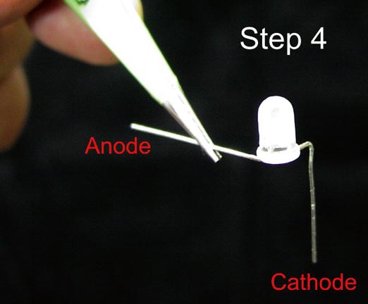
The anode should be closer to you, while the cathode should face outwards. From the base of the cathode leads, bend the lead outwards by 90 degrees along the line perpendicular to you (Figure 17).
FIGURE 17.
Next, bend the anode lead from its base by 90 degrees to the left, along a line parallel to you (Figure 18).
FIGURE 18.
Holding the leads from the middle portion is an efficient way of bending them. Now, the anode and cathode leads should be perpendicular to each other. Hold the bent cathode lead 1/4” from its base using needlenose pliers and make a 90 degree downward bend so the pliers are holding the cathode Lead (Figure 19). After bending the 64 LEDs in the above manner, we are ready to begin building the LED cube layers.
FIGURE 19.
Making Individual Layers
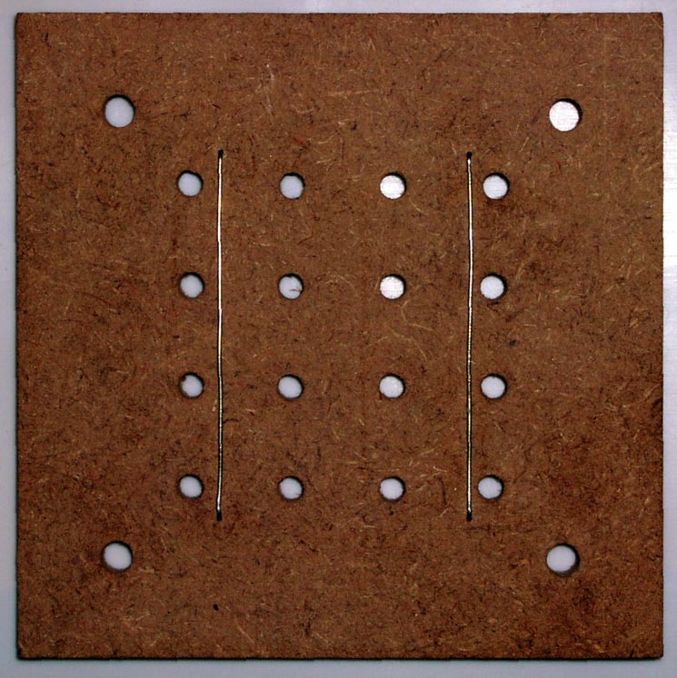
Orient the jig so that the 3/64” holes are at the top and bottom of the jig facing you. Each layer is made up of 16 LEDs.
Put two C shaped tin wires in place along the four 3/64” holes (Figure 20).
FIGURE 20. Jig base with two tinned wires loaded.
The small bent sections of each tin wire should go inside the 3/64” holes. The orientation of each tin wire is such that it is perpendicular to the anode lead’s horizontal lines and is vertical to you.
Insert the bent LEDs upside down into the top right corner 7/32” hole (Figure 21).
FIGURE 21. Jig base with two tinned wires and first LED loaded.
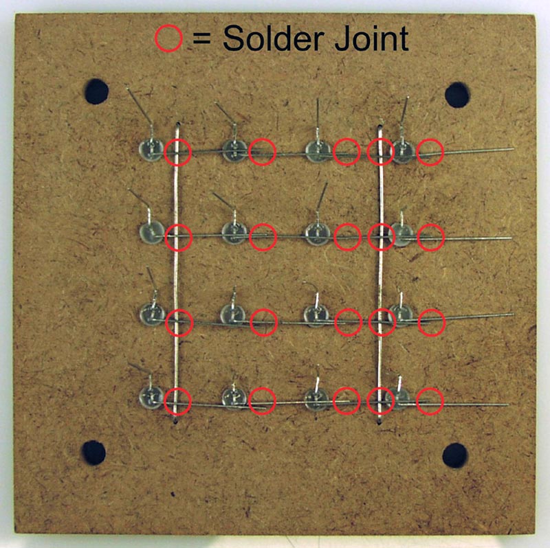
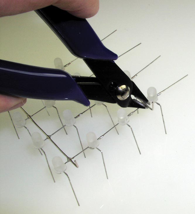
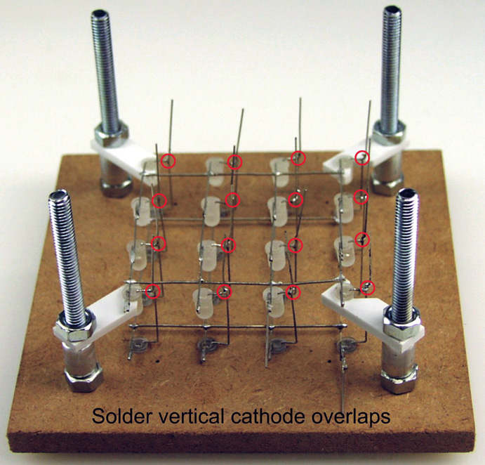
The LED should be oriented such that the bent anode lead (which rests parallel with the jig surface) is along the horizontal line parallel to you. Insert a second LED into the hole to the left of the previous one using the same orientation. Repeat this process for the rest of the LEDs. There are 16 7/32” holes. When all 16 LEDs are inserted (for each row of four LEDs), their bent anode leads should overlap some and form a horizontal line. The LEDs are soldered together at the overlaps as shown in Figure 22.
FIGURE 22. Layer 0 LED's loaded in jig base, red circles show solder joint points.
Solder the overlapping anode portions; there is a total of 12 solder joints. Solder the LED leads quickly since a longer contact period between the solder iron and the leads could damage the LED. Also remember to solder the eight solder joints where the two tin wires overlap the four horizontal anode lead lines. When you are finished, the LED layer may be removed from the jig (Figure 23).
FIGURE 23. Layer 0 soldered and removed from jig.
Cut off the extra portion of tin wire that went into the 3/64” holes (Figure 24).
FIGURE 24. Clipping ends of common anode wires.
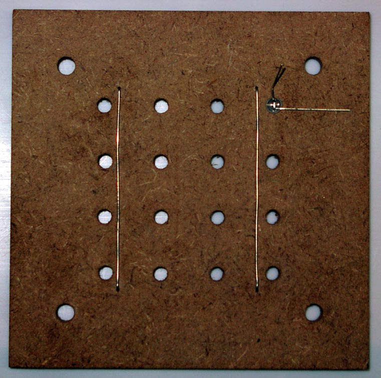
At this point, test the LEDs in the completed layer. To do so, touch the positive terminal to the uncut common anode lead on the right and the negative terminal to the upwardly bent cathodes one by one. Continue building three more layers in the same manner. Lift the layers from the jig carefully by pulling the bent cathode leads (Figure 25).
FIGURE 25. Bottom view of additional Layers.
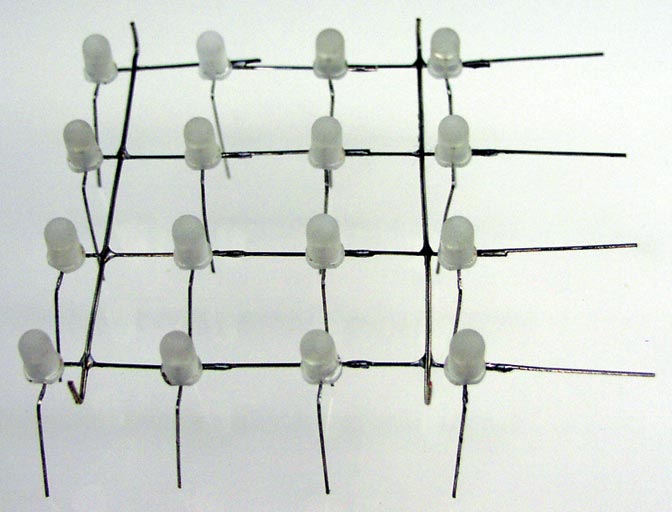
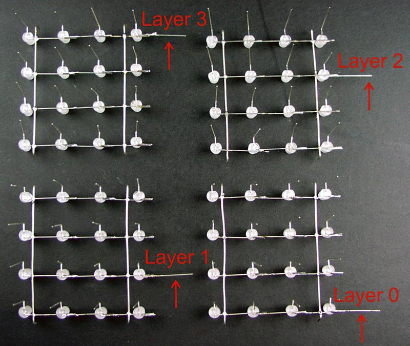
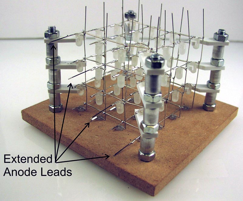
Notice in Figure 25 on the right-hand side of the layer that we have four extended anode leads. Each layer only needs one extended anode lead. Each layer differs from another in terms of the position of the uncut common anode layer lead; this is how we will be referring to the different layers from now on. Arrows in Figure 26 indicate the uncut common anode layer leads.
FIGURE 26. Bottom view of 4 layers, showing the extended anode lead for each layer.
Soldering Layers to Form the Cube
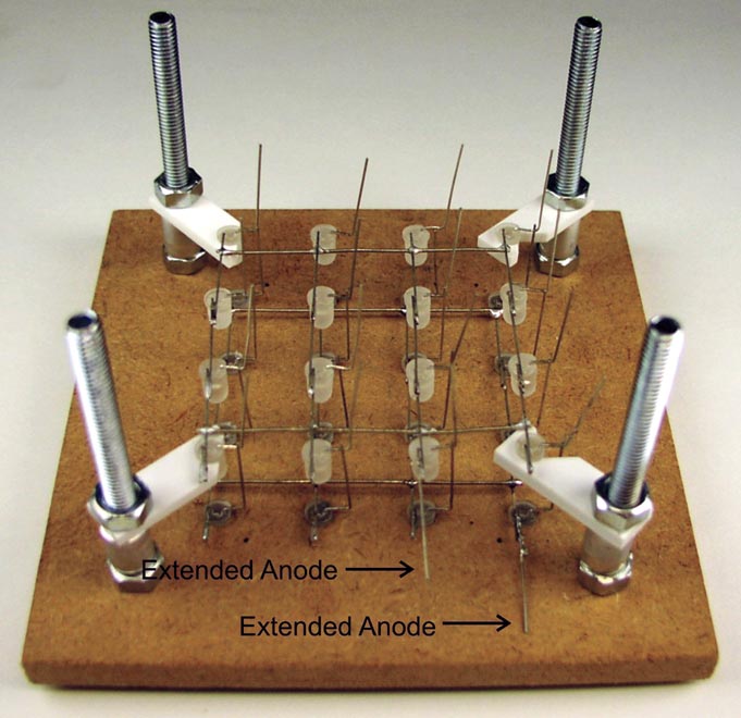
Insert four bolts into the four corner 1/4” holes. Secure each bolt to the jig using a 1/4-20 nut. Place LED Layer 0 in the jig holes. Pay attention to which side has the extended anode lead. Go to each bolt. On top of the existing nut, place a spacer, then on top of the spacer place an LED holder. Then, on top of the LED holders, put another 1/4-20 nut to secure everything down. Fasten Layer 1 into the LED holders. Keep the extended anode leads on the same side (Figure 27).
FIGURE 27. Layer 0 and Layer 1 in jig, showing placement of extended anode leads.
The bent cathode leads of the LEDs layers should overlap. If the cathode leads don’t touch each other, use narrow tweezers to bend them so they are in contact with the previous LED layers. Solder the overlapping cathode leads; there are a total of 16 cathode solder joints per layer as shown in Figure 28. The red circles highlight the vertical cathode solder joints for Layers 0 and l.
FIGURE 28. Layer 0 and Layer 1 in jig, red circules showing common cathode solder joints
Place Layer 2 with the four corner LEDs into the four corner hole’s LED holders (Figure 29).
FIGURE 29. Layers 0, 1, and 2 in jig.
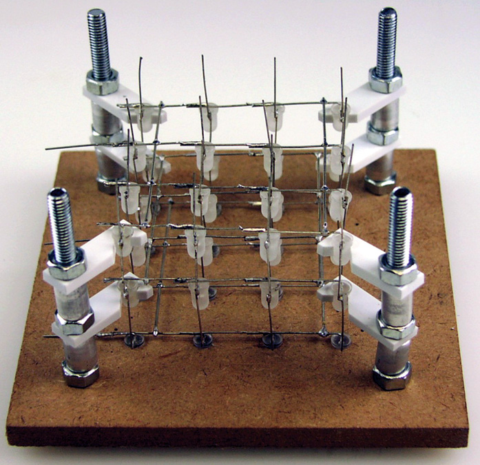
Solder the vertical cathode leads as before. Do the same thing for Layer 3. Notice how the extended anode leads are positioned on one side of the 3D LED matrix. The four extended common anode layer leads (one for each layer) end up in a staircase pattern (note the arrows). This is important for when we solder the matrix to the printed circuit board (PCB). You can test the LEDs before mounting the 3D LED matrix to the PCB. Unscrew all the nuts and remove the spacers and LED holders so you can get the LED matrix cube out of the jig. Your 3D matrix should look like Figure 30.
FIGURE 30. Layers 0, 1, 2 and 3 in jig, showing extended comman anode leads.
Cube PCB Construction
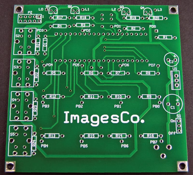
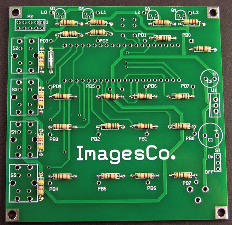
Now it’s time to mount the components on both sides of the PCB. The LED PCB is shown in Figure 31. The side with the text “ImagesCo.” is the top side of the board.
FIGURE 31. Top view PCB.
Mount and solder the components as described next. Depending on which color cube you select, the resistors R1, R2-R4, and R5-R16 will have different values. For the RED cube, the value is 220 ohms. For the YELLOW and GREEN cubes, the value is 180 ohms. For the BLUE cube, the value is 150 ohms.
On the top side of the PCB:
Mount resistors R1 (150/180/220 ohms), R5–R16 (150/180/220 ohms), R21–24 (4.7K ohms), and D1 (tin wire jumper in its place) on the top side (see Figure 32).
Mount resistors R2–R4 (150/180/220 ohms).
FIGURE 32. Top view PCB populated with resistors.
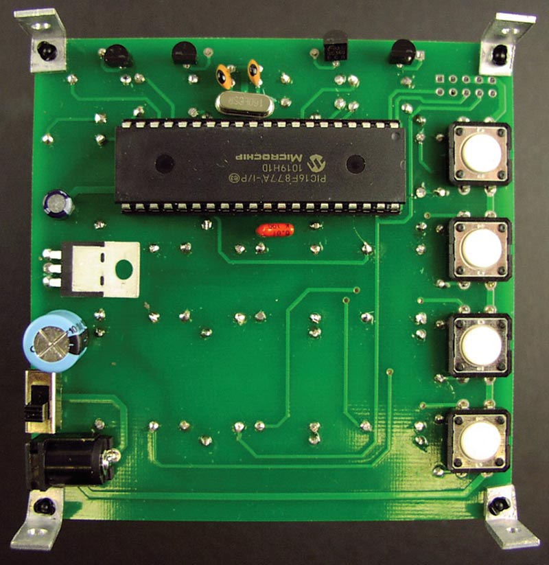
On the bottom side of the PCB:
Mount and solder R17–R20 (220 ohms) and crystal X1 (16 MHz).
Place the DIP 40-pin socket on the bottom side.
Place the capacitors C3 and C4 (22 pf).
Place capacitor C5 (0.1 µF).
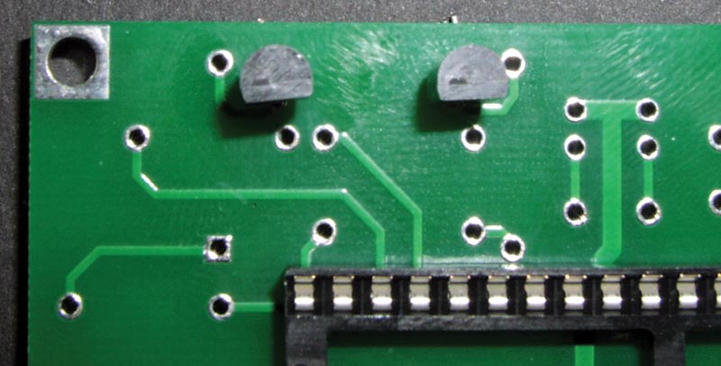
Mount transistors Q1–Q4 (BC 369) on the bottom side. The flat side of the transistor faces in toward the PCB. The curve/arc of the TO-92 transistor package faces outward from the PCB. Figure 33 shows a close-up of the transistors.
Mount the tactile switches S2–S5 onto the bottom side.
Mount the slide SPDT switch S1 onto the bottom side. The footprint is smaller than the switch lead pitch, so you will have to bend the outer leads slightly inwards using needlenose pliers.
Mount electrolytic capacitor C2 (47 µF/50V).
Mount electrolytic capacitor C1 (1,000 µF/16V).
Mount regulator U1 (7805) onto the bottom side. Bend the regulator inwards from the bottom side completely so that it touches the PCB. Cut the extra (unwanted) leads from the top side, and then solder the leads from the top side.
The 10-pin header P2 is optional and doesn’t have to be mounted. The DC barrel jack P1 should be soldered after the LED matrix is mounted on the top side.
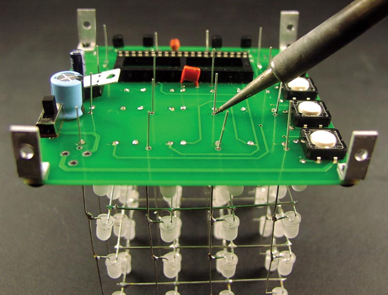
Insert the programmed PIC16F877A into the 40-pin DIP socket with the correct polarity on the bottom side of the PCB. You can use a pin straightener for easier insertion into the IC socket (see Figure 34).
Mount the four L brackets on the bottom side of the PCB with four small snap rivets. With the correct orientation, align the hole on the small arm of the L bracket to that of the mounting hole on the bottom side of the PCB. Place the small pop rivet from the top side into the mounting hole and press it until the rivet head touches the PCB. This will secure the L bracket into its place (see Figure 35).
FIGURE 33. Bottom view PCB, close up showing transistor orientation.
FIGURE 34. Bottom view PCB, populated.
FIGURE 35. Close up "L" bracket held with plastic push rivet.
Soldering the Cube to the PCB
Place the LED cube on the top side of the PCB with the correct orientation as shown in Figure 36.
FIGURE 36. LED matrix on PCB, extended anode above L0 to L3 pcb pads.
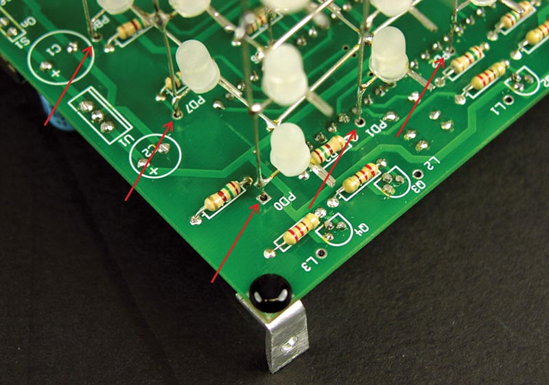
The uncut common layer anode leads should be facing the side of the board where the transistors are mounted. (See the edge of the PCB with four pads named L0, L1, L2, L3.) There will now be 16 pads named PD0 to PD7 and PB0 to PB7 for connection of the common cathode lines.
The 16 common cathode leads of the cube should be inserted into these pads using narrow tweezers. It would be helpful to tilt the cube a little and then insert the four common cathode leads by row. See a close-up in Figure 37.
FIGURE 37. Close up of LED matrix inserted into pcb pads.
Try to keep a distance of 1/2” between the PCB and the LEDs to avoid unwanted short circuits between the cube connections and PCB pads. Make sure the cube is symmetrically placed on the PCB. Now — with the exception of the pins PB7, PD2, and PD1 — the common cathode leads can be soldered on the bottom side. You will need to hold the cube PCB upside down to solder the common cathode pins on the bottom of it (see Figure 38).
FIGURE 38. Soldering LED matrix on bottom side of pcb.
Trim the excess wire from the soldered common cathode leads leaving a tiny portion from the roots, and then solder the pins. Solder PB7, PD1, and PD2 from the top side of the PCB. On the bottom side, cut PB7 flush to the PCB, and the PD1 and PD2 leads as short as you can.
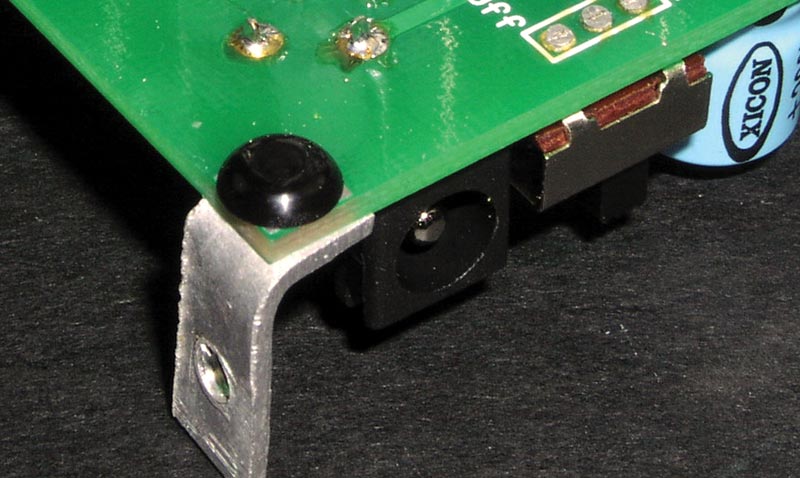
Place the P1 DC barrel jack on the bottom side. Since PB7 pin overlaps the P1 jack, it is necessary that PB7 is cut flush to the PCB (or else the jack won’t sit flush to the PCB which again means the jack wouldn’t sit in its place properly). The barrel jack pins are smaller than the hole diameters on the PCB, so make sure the jack is soldered such that it matches the component outline. Solder one of the pins of the jack on the bottom side.
Turn the PCB upside down and solder PB7 and the remaining P1 jack pins on the top side of the PCB. Also solder PD1 and PD2 from the top side of the PCB.
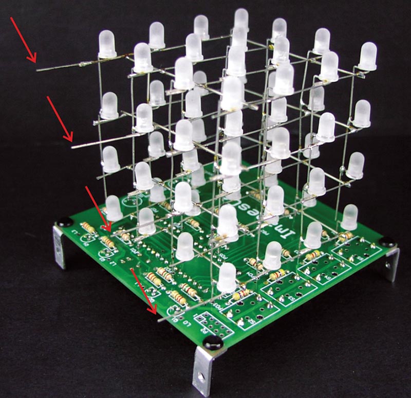
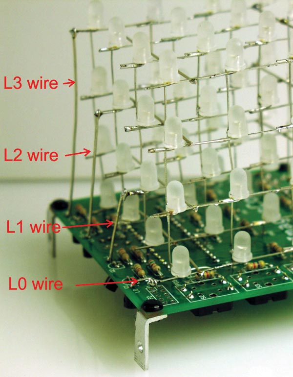
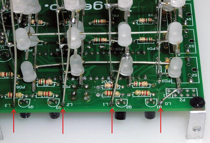
Now, the four common layer anode leads (the uncut staircase type leads; see Figure 36 again) need to be joined to their corresponding pads (L0, L1, L2, L3) on the PCB. Use straightened tin wire pieces to make the connections. The common anode to bottom Layer 0 is connected to pad L0. The common anode on Layer 1 is connected to pad L1. The common anode to Layer 2 is connected to pad L2. Finally, the top (Layer 3) common anode lead should be connected to pad L3. Next, trim the extended anode leads to the solder joints as shown in Figure 39.
FIGURE 39. Connecting common anodes to PCB using tinned wire.
A close-up of the anode connection wires going into the PCB pads is shown in Figure 40.
FIGURE 40. Close up of tinned wire soldered in the L0, L1, L2 and L3 pcb pads.
Transparent Case Mounting
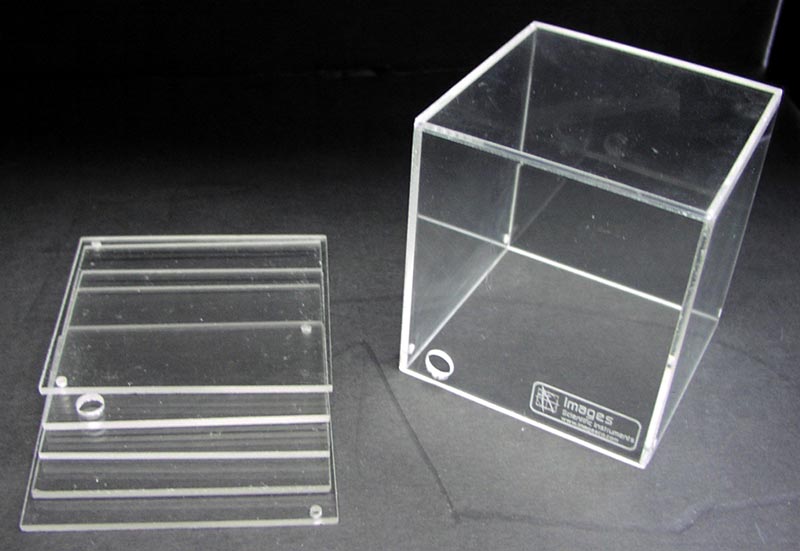
The LED cube can be used with or without an enclosure. There is an optional transparent case (Figure A) available in a (glue together) kit store.nutsvolts.com/project-kits/sku17056, however, you can design your own or ommit it altogether.
FIGURE A. Transparent case, assembled and unassembled.
The instructions for assembly are provided with the cube, so we will not repeat them here. The holes in the transparent case line up with the holes for the L brackets and the DC jack on the lower end.
When it’s time, you’ll slide the case over the cube (with the PCB) with the correct orientation so that holes for the L brackets and DC jack match with those on the PCB. Insert the plastic push rivets from outside of the case into the holes on the case that match with the L bracket long arm hole.
Operation
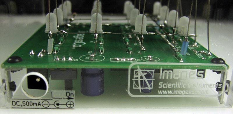
Insert the DC female jack into the male socket with the correct polarity and voltage/current ratings of the DC adapter (Figure 41). Slide the switch S1 to the on position by lifting the cube. Once powered on, the cube will blink all the LEDs five times before beginning to display the other patterns in the demo mode. Once all the patterns have been run, the process will start again.
FIGURE 41. Power connection.
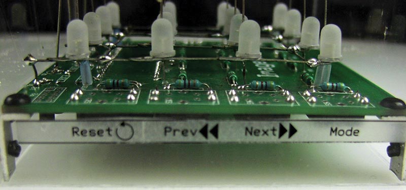
Pushbutton Controls
There are four pushbutton switches (S2 to S5) for various functions. These buttons can be accessed by lifting the cube since the switches are mounted to the bottom side of the PCB (see Figure 42).
FIGURE 42. Button Label.
The S2 switch is for reset. The S5 switch is the mode switch. Pressing it will toggle between the demo mode and user mode. In user mode, a single pattern will run over and over again.
S3 and S4 act as previous/next (cycle) pattern switches in user mode for selecting a particular pattern.
DIY 3D LED Cube Programming
Code for the 16F877A is provided in the downloads below. If you aren’t satisfied with the canned patterns provided in the PIC, you can try your hand at programming the LED cube yourself.
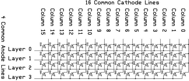
Programming the LEDs is not very difficult, but does take some thought. Look at Figure 43.
FIGURE 43. LED matrix schematic.
Here’s how our LEDs are wired inside the cube. We have common anode lines for each of the four layers. Each vertical column (1-16) consists of four vertical LEDs tied to a common cathode. We turn individual LEDs on and off by bringing the I/O lines of the PIC high or low. We control the current to the common anode lines using four I/O lines (RC0-RC3) connected to four power transistors. Bringing this line low will turn on the transistor, allowing current to flow into the common anode line to the LEDs. The individual LEDs are controlled by the I/O lines on port B and port D. Bringing a port I/O line low will turn on that LED.
Essentially, by controlling the I/O lines we can turn on any individual LED inside the 3D matrix, any group of LEDs inside the 3D matrix, or all of the LEDs inside the matrix. Patterns are created by sequencing LED patterns on and off rapidly. Here are some general rules:
A high output (1) on an I/O line on port D or port B will turn the LED off; low (0) will turn the LED on.
A low (0) on port C will make the PNP layer transistor turn on; a high (1) will turn it off.
Sixteen cathode rows can be turned on/off by the port pins directly (port B and port D).
Four anode columns can be turned on/off by the port pins via PNP drivers (port C).
Test Program Function
Layers are scanned one by one. When a particular layer is active, a two-byte/16-bit word is simultaneously outputted on the cathode pins.
Byte-sized variables are:
a[0] and a[1] are cathode data for Layer 0.
a[2] and a[3] are cathode data for Layer 1.
a[4] and a[5] are cathode data for Layer 2.
a[6] and a[7] are cathode data for Layer 3.
Layer 0 is the bottommost; Layer 3 is the topmost.
To create a pattern, set the frame repetition rate (the time one frame stays on). Load the appropriate frame data into the array variable and use a subroutine frameout for outputting the frame. Load the next frame data into an array variable and follow the same procedure.
alloff con 111111 ‘all cathodes off
allon con 000000 ‘all cathodes on
cubeoff con 001111 ‘all anodes off
layer0 con 001110 ‘layer 0 Floor enabled
layer1 con 001101 ‘layer 1 enabled
layer2 con 001011 ‘layer 2 enabled
layer3 con 000111 ‘layer 3 Top enabled
x var byte ‘x,z general variables
z var byte
a var byte [8] ‘array variable stores current
‘frame data for LED cathodes
frame var byte ‘single frame repetition rate variable
trisb = 0 ‘portb, pord connects to cathode,
‘portc connects to anode
trisd = 0
trisc = 0
portc = cubeoff ‘disable all layers (pnp drivers)
portd = alloff ‘initialize all cathode driving
‘ports to off condition
portb = alloff
inout: ‘inout pattern - a subset square
‘and outermost square turn on
‘alternately
frame = 24 ‘set frame repetition rate
a[0] = 111111 ‘set initial frame data
a[1] = 111111
a[2] = 011111
a[3] = 111001
a[4] = 011111
a[5] = 111001
a[6] = 111111
a[7] = 111111
inouti: ‘main loop of pattern
gosub frameout ‘ouput current frame
for z = 0 to 7 ‘invert frame data to
‘interchange squares
a[z] = ~a[z]
next z
goto inouti ‘go back to main loop
frameout: ‘main frame out subroutine
for x = 0 to frame ‘display patterm as per set
‘frame repetition rate
portd = a[0] ‘set ports connected to
‘cathode pins for Layer 0
‘frame data
portb = a[1]
portc = layer0 ‘enable layer 0 anodes
pause 4 ‘pause for layer on time -
‘set refresh rate to avoid
‘flickering
portc = cubeoff ‘disable all layers while
‘changing cathode data from
‘one layer to another
portd = a[2] ‘set ports connected to
‘cathode pins for Layer 1
‘frame data
portb = a[3]
portc = layer1 ‘enable layer 1 anodes
pause 4 ‘pause for layer on time -
‘set refresh rate to avoid
‘flickering
portc = cubeoff ‘disable all layers while
‘changing cathode data from
‘one layer to another
portd = a[4] ‘set ports connected to
‘cathode pins for Layer 2
‘frame data
portb = a[5]
portc = layer2 ‘enable layer 2 anodes
pause 4 ‘pause for layer on time -
‘set refresh rate to avoid
‘flickering
portc = cubeoff ‘disable all layers while
‘changing cathode data from
‘one layer to another
portd = a[6] ‘set ports connected to
‘cathode pins for Layer 3
‘frame data
portb = a[7]
portc = layer3 ‘enable layer 3 anodes
pause 4 ‘pause for layer on time -
‘set refresh rate to avoid
‘flickering
portc = cubeoff ‘disable layers while
‘changing cathode data from
‘one layer to another
next x
return ‘return to main program
end
Wrap-Up
The test program shows how to display a simple repeating pattern with the stored templates. Programs can also run live, meaning that the running program determines which LED or group of LEDs light next without reading the information from stored data within the program.
That concludes our 3D LED cube build. This project is a real attention-getter and I’m sure you’ll get many hours of enjoyment from it. I know I have. NV
A sharp eye’d reader (Barry Perkin) pointed out some mis-labeled components on the schematic for the LED cube. The PCB matched the text in the article. With this updated schematic, the schematic, text and pcb all match.