There's the old saying: “You can give a man a fish and he will eat for a day or you can teach a man to fish and he will eat forever.” There are many articles that give the reader a specific design for building a power supply, and there's nothing wrong with these cookbook designs. They often have very good performance. However, they don’t teach the readers how to design a power supply by themselves. This two-part article will start from the beginning and explain every step necessary to build a basic analog power supply. The design will focus on the ubiquitous three-terminal regulator and include a number of enhancements to the basic design.
It's always important to remember that the power supply — either for a particular product or as a general piece of test equipment — has the potential to electrocute the user, start a fire, or destroy the device it's powering. Obviously, these are not good things. For that reason, it's critical to approach this design conservatively. Provide plenty of margin for components. A well-designed power supply is one that is never noticed.
Input Power Conversion
Figure 1 shows the fundamental design for a typical analog power supply. It consists of three main components: input power conversion and conditioning; rectification and filtering; and regulation. The input power conversion is typically a power transformer and is the only method considered here. However, there are a couple of points that are important to mention.
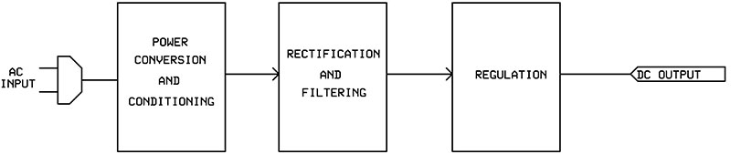
FIGURE 1. A basic analog power supply consists of three parts. The first two are discussed in this article and the last in the next installment.
The first is that 117 VAC (Volts Alternating Current) is really an RMS (Root Mean Square) measurement. (Note that I've seen ordinary household power specified anywhere from 110 VAC to 125 VAC. I just measured mine and found it to be precisely 120.0 VAC.) An RMS measurement of a sine wave is much lower than the actual peak voltage and represents the equivalent DC (Direct Current) voltage needed to provide the same power.
he RMS conversion varies according to the wave shape; for a sine wave, the value is 1.414. This means that the deviation around zero volts is actually 169.7 volts (for my 120 VAC power). The power goes from -169.7 volts to +169.7 volts each cycle. Therefore, the peak-to-peak voltage is actually 339.4 volts!
This voltage becomes especially important when adding bypass capacitors to the main power lines to suppress noise from entering or leaving the power supply (a common situation). If you think the actual voltage is 120 volts, you may use 150 volt capacitors. As you can see, this is not correct. The absolute minimum safe working voltage for your capacitors is 200 volts (250 volts is better). Don’t forget that if you expect to see noise/spikes on the line, you need to add that noise/spike voltage to the peak voltage.
The input frequency is universally 60 Hz in the USA. In Europe, 50 Hz is common. Transformers rated for 60 Hz will generally perform well on 50 Hz and vice versa. Additionally, the frequency stability of the power line is usually excellent and rarely a consideration. Occasionally, you may find 400 Hz transformers available. These are typically military or aeronautical devices and are generally not suitable for use on 50/60 Hz power (or vice versa).
The output of the transformer is also specified as an RMS voltage. Additionally, the voltage specified is the minimum voltage expected under full load. Often there is about a 10% increase in the rated output with no-load. (My 25.2 volt/two-amp transformer measures 28.6 volts with no load.) This means that the actual no-load/peak output voltage for my 25.2 volt transformer is 40.4 volts! As you can see, it's always important to remember that the rated RMS voltages for AC power are substantially less than the actual peak voltages.
Figure 2 provides a typical input power conversion and conditioning design. I prefer to use a double-pole switch although it's not absolutely necessary. It protects against miswired electrical outlets (which is rare today) or miswired power leads in the power supply itself (much more common). It's vital that when the power switch is off, the hot lead is disconnected from the power supply.
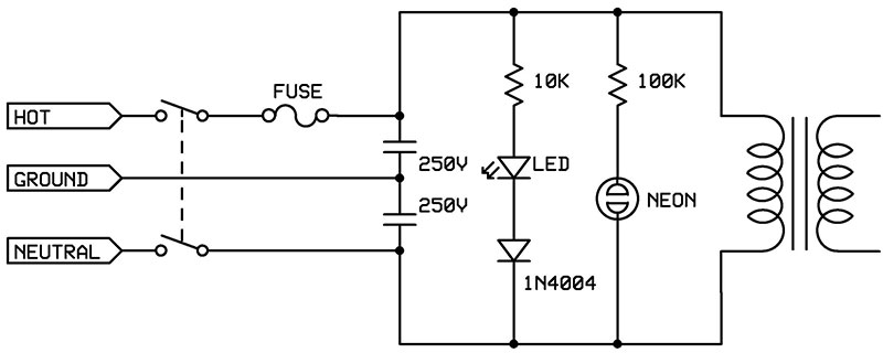
FIGURE 2. The input conditioning is pretty basic, but it must be remembered that the RMS voltage is not the same as the peak voltage. The peak voltage of 120 VAC RMS is about 170 volts.
The fuse (or circuit breaker) is necessary. Its main purpose is to prevent fires because without it, a transformer or primary circuit short will allow massive currents to flow causing metal parts to get red or even white hot. It's usually a slow-blow type rated at 250 volts. The current rating should be about double of what the transformer can expect to draw.
For example, the 25.2 volt two-amp transformer mentioned above will draw about 0.42 amps of primary current (25.2 volts/120 volts x two amps). So, a one amp fuse is reasonable. A fuse in the secondary will be discussed in the next article.
The bypass capacitors help to filter out noise and are optional. Since the peak voltage is about 170 volts, a 250 volt rating is better than a marginal 200 volt rating. You may want to use a “power-entry filter.” There are many types of these units. Some contain a standard power connector, switch, fuse holder, and filter in one small package. Others may have only some of these components. Typically, the ones with everything are fairly expensive, but surplus units can usually be found at very reasonable prices.
Being able to determine if the primary circuit is powered is important so a pilot light is used. Two typical circuits are shown. The neon lamp has been used for decades. It's simple and inexpensive. It has the drawbacks that it is somewhat fragile (being made of glass); can flicker if the resistor is too big; and can actually generate some electrical noise (due to the sudden ionic breakdown of the neon gas).
The LED circuit also requires a current-limiting resistor. At 10,000 hms, about 12 mA of current is provided. Most LEDs are rated for a maximum current of 20 mA, so 12 mA is reasonable. (High efficiency LEDs may work satisfactorily with only 1 or 2 mA, so the resistor can be increased as required.)
Note that LEDs have really poor reverse breakdown voltages (typically 10 to 20 volts). For that reason, a second diode is necessary. This must be able to operate with at least 170 volts of PIV (Peak Inverse Voltage). The standard 1N4003 is rated at 200 PIV which doesn’t provide much margin. The 1N4004 is rated at 400 PIV and costs perhaps a penny more. By placing it in series with the LED, the overall PIV is 400 plus the LED PIV.
Rectification and Filtering
Figures 3, 4, and 5 show the most typical rectification circuits with the output waveform displayed above. (The filter capacitor is not shown because by adding it, the waveform changes to something like a DC voltage.) It's useful to examine these three basic circuits to identify the strengths and weaknesses of them.
Figure 3 shows the basic half-wave rectifier. The only redeeming characteristic of this is that it's very simple, using only a single rectifier. The bad feature is that it uses only half of the power cycle making the theoretical efficiency of the circuit less than 50% just to start. Often, half-wave rectifier power supplies are only 30% efficient. Since transformers are expensive items, this inefficiency is very costly. Secondly, the wave shape is very difficult to filter. Half the time there's no power at all coming from the transformer. Smoothing the output requires very high values of capacitance. It's rarely used for an analog power supply.
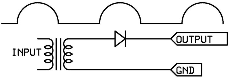
FIGURE 3. The half-wave rectifier circuit is simple but it produces a poor output waveform that is very difficult to filter. Additionally, half of the transformer power is wasted. (Note that the filtering capacitors are omitted for clarity because they change the waveform.)
An interesting and important thing happens when a filter capacitor is added to a half-wave rectifier circuit. The no-load voltage differential doubles. This is because the capacitor stores energy from the first half (positive part) of the cycle. When the second half occurs, the capacitor is holding the positive peak voltage and the negative peak voltage is applied to the other terminal causing a full peak-to-peak voltage to be seen by the capacitor and through that, the diode. Thus, for a 25.2 volt transformer above, the actual peak voltage seen by these components can be over 80 volts!
Figure 4 (top circuit) is an example of a typical full-wave/center-tap rectifier circuit. When this is used, in most cases, it probably shouldn’t be. It provides a nice output that is fully rectified. This makes filtering relatively easy. It uses only two rectifiers, so it’s pretty inexpensive. However, it's no more efficient than the half-wave circuit presented above.
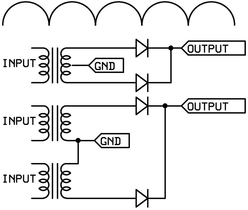
FIGURE 4. The full-wave design (top) produces a nice output. By redrawing the circuit (bottom), it can be seen that it's really just two half-wave rectifiers connected together. Again, half the transformer power is wasted.
This can be seen by re-drawing the circuit with two transformers (Figure 4 bottom). When this is done, it becomes clear that the full-wave is really just two half-wave circuits connected together. Half of each transformer power cycle is not used. Thus, the maximum theoretical efficiency is 50% with real efficiencies around 30%.
The PIV of the circuit is one half of the half-wave circuit because the input voltage to the diodes is half of the transformer output. The center tap provides half the voltage to the two ends of the transformer windings. So, for the 25.2 volt transformer example, the PIV is 35.6 volts plus the no-load increase which is about 10% more.
Figure 5 presents the bridge rectifier circuit which should generally be the first choice. The output is fully rectified so filtering is fairly easy. Most importantly, however, it uses both halves of the power cycle. This is the most efficient design and gets the most out of the expensive transformer. Adding two diodes is much less expensive than doubling the transformer power rating (measured in “Volt-Amps” or VA).
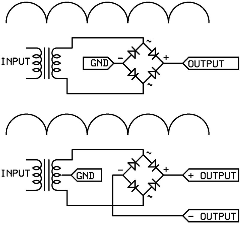
FIGURE 5. The bridge rectifier approach (top) provides full use of the transformer power and with a full-wave rectification. Additionally, by changing the ground reference (bottom), a dual voltage power supply can be obtained.
The only drawback to this design is that the power must pass through two diodes with a resulting voltage drop of 1.4 volts instead of 0.7 volts for the other designs. Generally, this is only a concern for low voltage power supplies where the additional 0.7 volts represents a substantial fraction of the output. (In such instances, a switching power supply is usually used rather than either of the above circuits.)
Since there are two diodes being used for each half-cycle, only half of the transformer voltage is seen by each. This makes the PIV equal to the peak input voltage or 1.414 times the transformer voltage, which is the same as the full-wave circuit above.
A very nice feature of the bridge rectifier is that the ground reference can be changed to create a positive and negative output voltage. This is shown in the bottom of Figure 5.
| Circuit |
Filter Needs |
PIV Factor |
Transformer Use |
| Half-Wave |
Large |
2.82 |
50% (theoretical) |
| Full-Wave |
Small |
1.414 |
50% (theoretical) |
| Bridge |
Small |
1.414 |
100% (theoretical) |
TABLE 1. A summary of the characteristics of the various rectifier circuits.
Filtering
Nearly all filtering for an analog power supply comes from a filter capacitor. It's possible to use an inductor in series with the output, but at 60 Hz, these inductors must be quite large and are expensive. Occasionally, they are used for high-voltage power supplies where suitable capacitors are expensive.
The formula for calculating the filter capacitor (C) is quite simple, but you need to know the acceptable peak-to-peak ripple voltage (V), half-cycle time (T), and current drawn (I). The formula is C=I*T/V, where C is in microfarads, I is in milliamps, T is in milliseconds, and V is in volts. The half-cycle time for 60 Hz is 8.3 milliseconds (reference: 1997 Radio Amateur’s Handbook).
It's clear from the formula that the filtering requirements are increased for high current and/or low ripple power supplies, but this is just common sense. An easy-to-remember example is 3,000 microfarads per ampere of current will provide about three volts of ripple. You can work various ratios from this example to provide reasonable estimates of what you need fairly quickly.
One important consideration is the surge of current at turn-on. The filter capacitors act as dead shorts until they get charged up. The larger the capacitors, the greater this surge will be. The bigger the transformer, the greater the surge will be. For most low voltage analog power supplies (<50 volts), the transformer winding resistance helps somewhat. The 25.2 volt/two amp transformer has a measured secondary resistance of 0.6 ohms. This limits the maximum inrush to 42 amps. Additionally, the inductance of the transformer reduces this somewhat. However, there is still a large potential current surge at turn-on.
The good news is that modern silicon rectifiers often have huge surge current capabilities. The standard 1N400x family of diodes is usually specified with 30 amps of surge current. With a bridge circuit, there are two diodes carrying this, so worst-case is 21 amps each which is below the 30 amp specification (assuming equal current sharing, which is not always the case). Tthis is an extreme example. Generally, a factor of about 10 is used, instead of 21.
Nevertheless, this current surge is not something to be ignored. Spending a few cents more to use a three-amp bridge instead of a one-amp bridge may be money well spent.
Practical Design
We can now put these rules and principles to use and start to design a basic power supply. We'll use the 25.2 volt transformer as the core of the design. Figure 6 can be seen as a composite of the previous figures but with practical part values added. A second pilot light in the secondary indicates its status. It also shows if there's a charge on the capacitor. With such a large value, this is an important safety consideration. (Note that since this is a DC signal, the 1N4004 reverse voltage diode is not needed.)
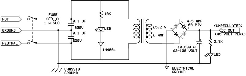
FIGURE 6. Final design of the power supply with practical parts specifications. Regulating the power is discussed in the next article.
It may be cheaper to use two smaller capacitors in parallel than one large one. The working voltage for the capacitor must be at least 63 volts; 50 volts is not enough margin for the 40 volt peak. A 50 volt unit provides only 25% margin. This may be fine for a non-critical application, but if the capacitor fails here, the results can be catastrophic. A 63 volt capacitor provides about a 60% margin while a 100 volt device gives a 150% margin. For power supplies, a general rule of thumb is between 50% and 100% margin for the rectifiers and capacitors. (The ripple should be about two volts, as shown.)
The bridge rectifier must be able to handle the high initial current surge, so spending an additional dime or two for improved reliability is worthwhile. Note that the bridge is specified by what the transformer can supply rather than what the power supply is eventually specified for. This is done in case there's an output short. In such a case, the full current of the transformer will be passed through the diodes. Remember, a power supply failure is a bad thing. So, design it to be robust.
Conclusion
Details are an important consideration in designing a power supply. Noting the difference between RMS voltage and peak voltage is critical in determining the proper working voltages for the supply. Additionally, the initial surge current is something that cannot be ignored.
In Part 2, we'll complete this project by adding a three-terminal regulator. We'll design a general-purpose, current-limited, adjustable voltage power supply with remote shut-off. Additionally, the principles used for this design can be applied to any power supply design. NV
A Note on Efficiency
Let me explain the difference between a full-wave rectifier design and a bridge — especially from the point of view of efficiency.
Remember I said half the power is wasted with a full-wave rectifier design. It's self-evident if you consider that a full-wave design is really made up of two half-wave designs. Combining two circuits that are each about 50% efficient doesn't in any way increase the total efficiency of the circuit. It’s still about 50% overall.
The loss of efficiency comes from the amplitude of the resultant rectification. A half-wave circuit clearly provides half the amplitude that is available from the transformer. So does the full-wave version, but it’s not as obvious. It only uses half of the total available voltage of the transformer.
The output of the full-wave rectifier is 1.414 times the voltage between the center tap and the end. The output of a bridge is the full end-to-end voltage of the transformer times 1.414. This is shown in Figure A.
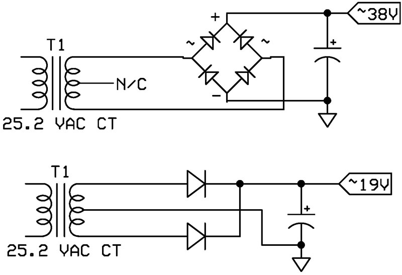
FIGURE A.
For the 25.2 volt transformer, the full-wave rectifier develops about 19 volts (unloaded). The bridge rectifier develops about 38 volts (unloaded). So, the full-wave rectifier does indeed waste about half the available power from the transformer.