Over the years with different companies I have worked for, I always had access to high-end audio THD (Total Harmonic Distortion) analyzers. I found these very useful for design work, debugging, and repair of audio equipment. My present company has no need for them and consequently they aren’t included in their armory of test equipment. Oftentimes, I have need for one but could never afford to own one — not even a used one. I thought this would be a worthwhile project, so the following article will describe my experience and all the details on how to construct one if you so desire.
I had never delved into the internal details of these instruments but did know the basic architecture of how they operated. After working with RF well into the VHF and UHF bands for the last several years and with all the problems involving high frequency RF in bringing completed designs into the real world, I thought working down at the audio level would be “a day at the beach.” WRONG! I spent about a week analyzing the circuit designs of many commercial units and was absolutely amazed at the precision and stability that went into them. My first thought was that I didn’t think I could build one that could even come close to matching their specs — at least not on a shoestring budget. However, giving this a little more thought, I realized I don’t need to match those specs, but rather build a scaled down version that would fulfill the needs of the average audio enthusiast yet still give acceptable performance.
So, I drew up a design that would have acceptable performance and laid down the target specs I wanted to achieve. Before I continue along those lines, let’s talk a little bit about audio and give you a clearer picture of why I designed my analyzer the way I did.
As I mentioned, some commercial units have an incredible level of performance, but do we really need that level? We have all seen advertised specs of 0.001% THD or even better on some audio amplifiers, which is a great work of design but probably an overkill for most listeners.
Consider this. In the total processing of audio reproduction from start to end, there is some small distortion created in the audio to electrical transducer (mic), then capturing that signal onto vinyl, discs, or whatever further adds its share. It’s played back through the “perfect” amplifier which may contribute such low distortion as to be almost immeasurable. From this point, it drives a speaker system, and even high-end speakers and enclosures could contribute 2% of distortion — not to mention a less than ideal crossover circuit. Last (but not least) is the listening environment which can definitely alter the audio sound waves before we hear them.
You can see by now that the “distortion-less” amplifier specs have been swamped out several orders of magnitude by other components in the chain. Now for the topper: You will notice that up to this point I haven’t mentioned the stand-alone word of SOUND. Amplifiers reproduce electrical signals, and speakers convert this to physical sound waves. However — as of yet — no sound has been produced.
Sound has neither electrical or physical properties. It’s a sensation that can only occur between the ear drum and brain of the human body. This is where everything becomes highly subjective. If a hundred people listened to the same perfect audio system, there would be a hundred slightly different takes on it — subjectiveness!
Now, don’t get me wrong as the pursuit of perfection in all of this audio equipment is an admirable trait and to a point worth the effort, but other than the highly trained ear of a musician or audiophile, the greater majority of us can’t recognize distortion beyond certain levels (some will actually prefer a little distortion).
In many years of looking at oscilloscope displays of sine waves, I have developed a pretty good eye for sine wave distortion. I can see distortion down to about three or four percent, but no further. However, I can hear that distortion when played though an audio system.
If I really strain my ears, I can detect distortion down to 1%; maybe approaching 0.5% — MAYBE! Beyond that level, it could be 0.5% or 0.0005% and I can’t hear the difference. I do appreciate good music and good sound systems, and feel that 99.9% of listeners fall into my same level of discrimination in those regards.
With that said, I chose my target specifications based on those facts. They were as follows:
- Relatively simple to build and well affordable.
- Adequate features and controls for easy operation.
- Spot-checking the audio spectrum at three points rather than continuous coverage.
- Three built-in low distortion signal sources to match three rejection filters.
- Capable of reading less than 0.5% distortion levels.
- Adequate range of output signal levels to the DUT (device under test).
- Adequate amplification/attenuation to handle a range of input signal levels to and from the DUT.
All these targets were successfully accomplished!
INSTRUMENT ARCHITECTURE
Distortion analyzers inject a low distortion sine wave into the input of the DUT and then extract that signal somewhere downstream from that point. The signal is fed into a very sharp notch filter to null out only the original sine wave frequency. Anything that remains is distortion products; noise and hum that were created in the DUT. That level is compared to the level of the extracted signal prior to the filter and converted to a numerical, percentage, decibel figure, or whatever is desired, and displayed on a readout.
My analyzer consists of three major sub-assemblies: a low distortion oscillator board containing three sine wave generators of nominal frequencies of 100 Hz, 1 kHz, and 10 kHz; a notch filter board of three filters that match those oscillators; and a control board with associated front panel controls. Plus, of course, a power source. Front panel controls are adequate without becoming overly excessive, so that operation is quick and easy. The whole package fits into a small housing and with proper shopping can be built relatively cheap. I built the internals up on four separate boards and would advise you to do the same as it makes construction and testing so much easier. The boards are: oscillator, filter, control, and power supply. I’ll discuss the oscillator and filter boards in detail and only touch upon the remaining two boards as they are so straightforward they need minimal explanation.
A couple of cautions before I start: This is not a piece of test equipment for true audiophiles as it would never test to their high standards. It’s also not a project for beginners, only because they may not have acquired the necessary test equipment yet that is needed in checkout and calibration. However, they may want to save this article for future reference because they won’t be beginners forever.
THE OSCILLATOR BOARD
There are three separate sine wave oscillators on this board; nominally 100 Hz, 1 kHz, and 10 kHz as viewed in Figure 1. I spent a fair amount of time in researching oscillators, but none of them really filled my needs. The standard Wien bridge style is relatively stable and pure, but requires a filament bulb (or other automatic amplitude correction) to operate properly.
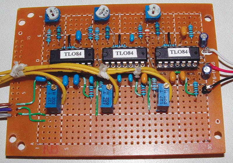
FIGURE 1. Oscillator board.
In years past, bulbs were available in every size and style one could imagine, but today they have virtually disappeared from the market. Those that remain are quite expensive and may not even be available for the exact one needed. They also draw a lot of current which causes loading problems. On the upper end of choices are designs built using state variable principles which give excellent performance. However, for best results, you should use a chip designed for just this purpose. The chip is a UAF42 and retails for $17 a pop. So, three onboard oscillator chips would be $51 just for starters and still need a fair amount of support circuitry — just too expensive.
Both these oscillators have a major advantage over most in that they are easily tunable over a wide range of frequency. My design uses a fixed frequency, so that would be of no advantage here.
I remembered an oscillator circuit I’ve used in the past: the less publicized “Bubba” oscillator. Technically speaking, this is a fourth order buffered filter with a gain stage and is connected to form a closed loop. Practically speaking, it’s an oscillator using four RC networks that are isolated from each other so as to provide a 180 degree phase shift. By buffering each RC stage, they are completely isolated from each other. This makes design and operation much simpler and straightforward.
The only requirements are that it follows certain rules known as the Barkhausen Criteria (shown in Figure 2). In simple terms, for any given linear sine wave oscillator, the circuit must have a gain of one and have 360 degrees of phase shift for every signal transition through the loop. In the Bubba circuit, the phase shift network uses four separate RC networks that each contribute 45 degrees of phase shift for a total of 180 degrees. The inverting amplifier adds an additional 180 degrees of phase shift for a total of 360 degrees. That satisfies one half of the criteria.
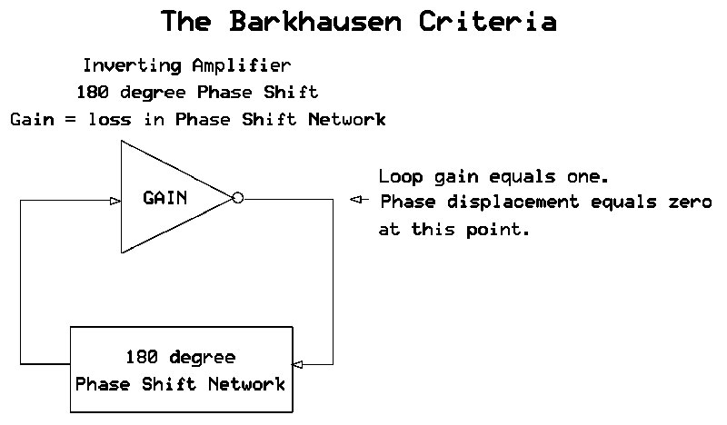
FIGURE 2. Barkhausen Criteria.
For a 45 degree shift in the RC network, the impedance of the R leg must equal the impedance of the C leg at the given frequency. The amplitude at its junction will be 0.707 of the input level (a loss). If we multiply 0.707 by itself four times, the last stage now has a level of 0.2401 of the input signal. This equates to a loss of 4.165.
If the gain in the inverting amplifier is made to be 4.165, the losses are corrected and the overall circuit gain is one. This satisfies the Barkhausen Criteria and the circuit will now oscillate. Of course, with real world components, nothing is exact. So, the gain must be slightly adjusted.
One thing you may be wondering about at this point is how do these circuits even oscillate since at power-up they have no signal to work off. Believe it or not, the secret is noise. All active and passive components produce a certain amount of noise, and the spectrum of that noise will be the bandwidth of that particular circuit.
At start-up, noise is produced, and no matter how minuscule it is, it still presents a signal. Buried in that mess is the one frequency of interest. Each trip around the loop it gets amplified over and over until it finally reaches the level for which the circuit was designed. This could take micro seconds or whole seconds to reach stability. It’s interesting to see a slow startup displayed on an oscilloscope that may take five or 10 seconds.
Figure 3 is the oscillator schematic. Since all three oscillators are laid out the same, only one print is needed for this with component values for each shown in the upper right. I know that any oscillator with a tag of “Bubba” doesn’t instill much confidence in its ability to perform very well, but the exact opposite is true. When properly adjusted, it has low distortion products approaching 0.1% and great stability — not too shabby for an RC oscillator. Its only disadvantage is wide range tuning requiring four pots in place of R1-R4 that must be tuned simultaneously and track each other very closely.
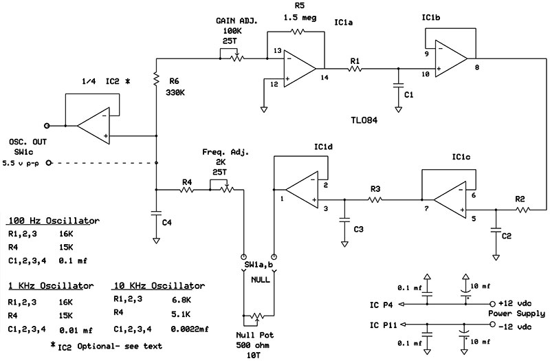
FIGURE 3. Chassis schematic.
Again, not a problem in this design (fixed frequency). As previously described, it follows the Barkhausen rule of phase shift and gain. Components R1,C1 through R4,C4 set the 180 degree phase shift required with all the IC1 stages, providing excellent buffering. IC1a provides the necessary gain to cover all the losses through the phase shift network. The gain required in IC1a is critical and can vary somewhat from one oscillator to another due to component tolerances, dielectric losses, and stray capacitance.
For that reason, a large value gain trimmer was needed to cover all the bases. In Figure 1, you’ll notice that these trimmers (white) are installed and are single-turn. These made adjustment a little difficult and have since been changed to 25-turn pots as shown in the schematic diagram.
This circuit will need a small range of frequency tuning to make up for all the component tolerances. That is accomplished at the last RC filter in the output of IC1d. The 2K Freq Adj and the Null Pot along with R4 change the time constant to correct all upstream errors in component tolerances. This 2K pot is the coarse adjustment and once set needs no further tuning.
The Null Pot located on the front panel is for fine-tuning to cancel out the fundamental frequency as much as possible when the instrument is in test mode. Notice that the Null Pot is the first resistance in this chain and connected to the output of IC1d. This positions a fairly large component and associated wiring that is prone to picking up noise into a low impedance environment which will attenuate most pickup. You can expect an output signal of 5.5V P-P, but it does vary between individual oscillators.
Also notice that IC2 of Figure 3 has been asterisked and listed as optional. Since I wanted to have easy access for reworking the boards as may be needed due to the circuitry being transferred to its final home and layout, the output-to-chassis leads were left quite long and bundled and laced. These leads come right out of a filter path that leaves them vulnerable to stray pickup and noise that may be present. For that reason, I later isolated them through an onboard buffer chip (not shown in Figure 1).
If the layout was such that short stiff leads were used here and formed away from each other in the soldering process, or pots and switches directly soldered to the circuit board, the oscillator outputs could just be taken directly from the filter as shown by the dashed line, thereby eliminating IC2. However, the buffer (if added) uses very little board real estate, is very quick and easy to wire up, and only adds 50 cents to the cost.
It uses three sections of a quad op-amp; the unused amp is wired as a follower with the plus input grounded to keep it quiet. The labeled oscillator frequencies of 100 Hz, 1 kHz, and 10 kHz are for convenience only as you will have to jump through a lot of hoops to get them right on the money. Fortunately, the audio amplifier being tested doesn’t know or care if that frequency is off a tad from what it’s labeled, just as long as it’s near the portion of the audio spectrum chosen; 5% one way or the other is acceptable and mine were within 1.5% of the target.
The resistors are 1% metal film and quite stable. The capacitors are 5% ceramic COG types, and these are about as good as it gets. They have very low temperature coefficients at about 30 PPM/degree C. Also, they are of high audio quality (yes, caps can produce audio distortion) which in audio amp applications may go completely unnoticed, but when it comes to instrument applications, every little improvement becomes important. COG is the key word here. In reality, 1% resistor tolerance is not close enough; even 0.1% is doubtful, so trimmer pots are the only way to bring it all together for desired operation.
One closing note here is that the oscillator board will be the second board to build. The filter board will be first and really dictate what the oscillator frequency needs to be. Why? Because it’s much easier to tune the oscillator than the filter frequency.
THE FILTER BOARD
As with the oscillator board, there are three separate filters on this board as seen in Figure 4. I mulled over which type of filter I would use in this application and decided on the “twin-T” type due to its superior notching capability. It also is a ‘lossless” filter meaning that all frequencies except the one of interest are passed through with no attenuation, which makes for easier circuit design. Its only disadvantage is that it’s hard to tune over a wide frequency range, but again, for this application, it’s of no concern since it always sees a fixed frequency. However, it can be tuned over a very small frequency range for final adjustment.
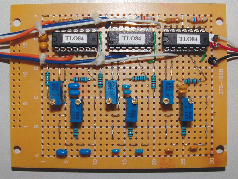
FIGURE 4. Filter board.
The filter’s job is to remove as much of the pure test sine wave extracted from the DUT’s output as it possibly can and nothing else. Leftover frequency components are junk that has been produced in the DUT and will be measured and quantified as to %, db, etc. This is known as “notching” and hence the name notch filter.
Notch filters are just a version of common high-pass, low-pass, and band-pass filters that we have all seen. However, there are some cautions to be taken for this application. Referring to Figure 5, it shows various results for a notch filter tuned to 1.000 Hz; Figure 5A shows a low-pass and a high-pass filter with their roll-off frequencies somewhat spread apart.
If using the familiar band-pass vs. center frequency formula to determine ‘Q’ (Quality factor), this filter has a low Q, but notice how deep the rejection notch can be. The rejection notch depth is the point where the vertical slope of each filter intercepts one another and cancels out any further drop in the notch. Also notice that the -3 db point in the filter’s knee is at 2.000 kHz. This would be unacceptable for THD testing as it’s starting to attenuate the second harmonic (2 kHz) of the 1 kHz fundamental and will display a test reading of that harmonic 3 db lower than what is really occurring at that point.
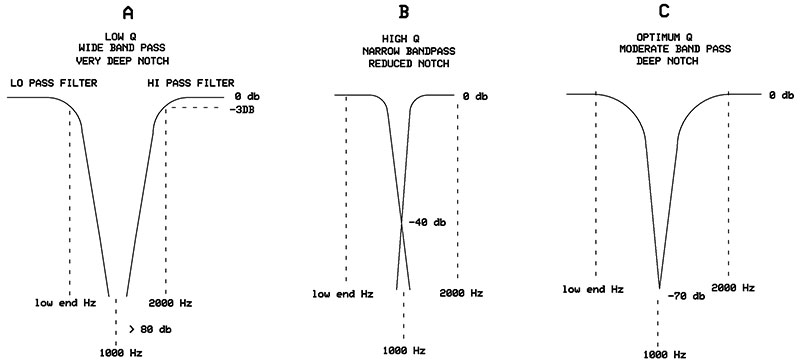
FIGURE 5. Filter characteristics.
Let’s shoot for a higher Q by pushing those two filters closer together as is shown in Figure 5B. Great! We now have a nice flat response at the 2 kHz point which will not attenuate the second harmonic response. Look what happened to the notch, though. The crossover of the slopes is now much higher and the notch depth is unacceptable. So, as is in much electronic design, a trade-off must be made here.
By adjusting the Q (as shown in Figure 5C) so that the filter’s response is such that the top of the knee just barely touches the 2 kHz portion of the spectrum and has no effect on second harmonic response — yet still gives acceptable notching — we have arrived at the optimum point.
The Q turns out to be in the neighborhood of 2.4 and the optimum resistance values have been calculated as R4 and R5 in the filter schematic to accomplish this. These charts and ratios hold true for all the filters; only the frequencies change.
Figure 6 shows the filter board schematic. Only one is drawn for simplicity, with individual component values for each filter shown in the upper right. The circuit is pretty straightforward, with two quadrants of the op-amp used for the actual filter and the other two used as buffers to the outside world.
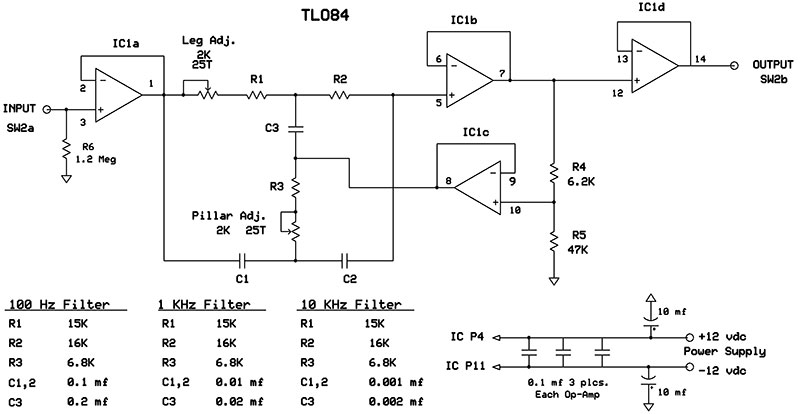
FIGURE 6. Filter schematic.
Twin-T filters like a low impedance source for their input and working into a high impedance at their output, so the two sections of the op-amp work out perfect here. As in the oscillator board, 1% metal film resistors and 5% ceramic COG capacitors are mandatory. Again, tolerances required are tighter than available components, so several trimmers are required.
The values of the output leg R2,C2 are fixed and the 2K trimpot ‘Leg Adj’ is for adjusting the time constant of the input leg to match the output leg. The 2K trimpot ‘Pillar Adj.’ is to adjust the vertical leg to match. As mentioned, IC1a is the input buffer and IC1b provides the high impedance for the filter output and drives the resistive divider R4,R5.
This divider applies the optimum level of the filter output signal for driving IC1c which is used in a ‘bootstrap’ configuration. Think of bootstrapping as reaching to grab your own boot straps and then pulling yourself up as high as you can to make yourself taller. Ridiculous I know, but that’s the only simplified analogy I could think of as to bootstrapping raising the level of notching performance, which is actually a type of feedback.
This circuit also sets the Q of the filter. IC1d merely buffers the whole assembly to enter the outside world. This output is then sent through a switching configuration and directly to the readout device: scope, meter, etc.
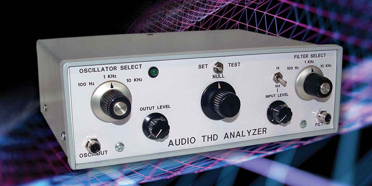
CONTROLS AND CHASSIS WIRING
The chassis layout shown in Figure 7 is the completed unit. This is where all the boards, switches, and controls get tied together.
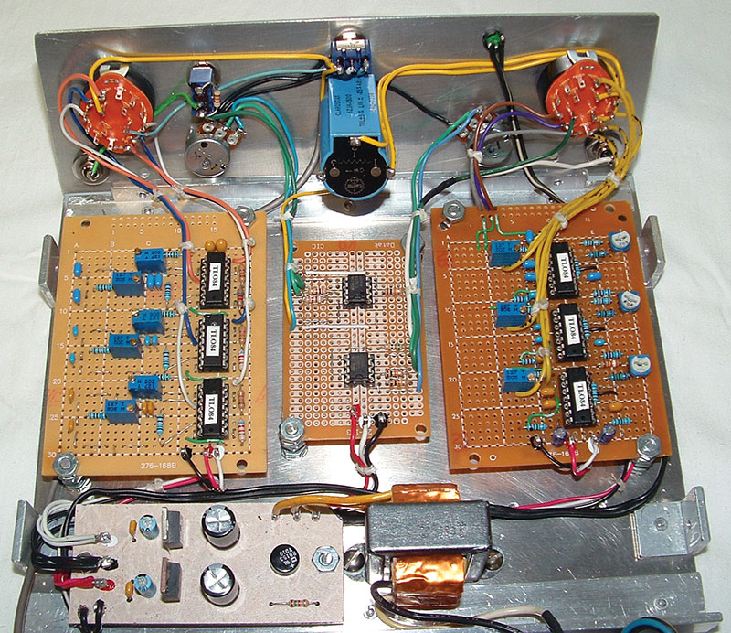
FIGURE 7. Chassis.
Referring to the schematic diagram in Figure 8, the oscillator and filter boards are shown only in block format since their schematics are in Figures 3 and 6, respectively. This simplifies the overall design for this instrument and gives a clearer layout for construction. IC1, IC2, and associated components comprise the control board which is shown in the center of Figure 7. The oscillator board and filter board are placed at opposite sides of the chassis and each has its own selector switch.
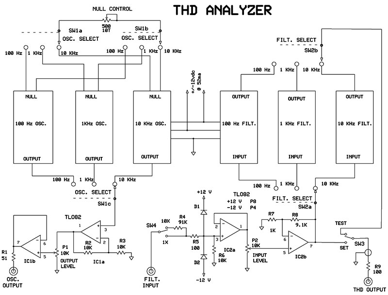
FIGURE 8. Chassis schematic.
I could have wired all of them together in a common switch and eliminated one (switch), but I elected to do it the way shown for several reasons. The single switch method would require a very expensive multi-deck wafer switch. Due to the amount of wiring and switching requirements, I wanted to keep each board’s wiring isolated from each other as much as possible to avoid any unwanted crosstalk (some crosstalk still shows up; it’s inevitable but at a very low level). This also separates these two functions for other types of testing.
The only disadvantage of wiring it up in this fashion is you must track two switches when changing frequencies, which is really no bother at all. IC1 and IC2 were separated for the same reason.
The oscillator PCB will have three wires per oscillator (nine total) coming out of the board: two each for the NULL control and one each for the output. The frequency of test is selected by SW1: a three-pole/three-position wafer switch labeled OSC SELECT.
SW1a and SW1b connect the NULL control to the selected oscillator; SW1c connects the output to the control board at IC1a and is amplified by a factor of two. This raises the 5V P-P level to 10V P-P. This was arbitrarily chosen to produce a level that might be needed for any given situation. This level could be raised to a higher level by decreasing R2. However, I wouldn’t go any higher than 15V P-P at this point (R2 = 6.2K) because we don’t want to introduce any distortion. This level keeps the voltage swing well below the chip’s power supply rails.
This output feeds a 50K level control and the wiper arm fed to IC1b: a buffer for the OSC OUTPUT jack. When coupling to an unspecified load, it’s always good practice to add a small series resistor in the output lead to keep the buffer stabilized under any conditions that could present themselves — especially high capacitance loads. I had calculated 50-100Ω for R3 and decided on 51Ω just to make the source impedance conform to a standard value. The output drive from this stage should be held to no more than 2 mA; that would equate to a 200Ω minimum load per V P-P, i.e., 1,000Ω load/5V P-P max signal.
The filter PCB will have two wires per filter (six total) coming out of the board: one each for input and one each for output. The filter frequency of test is selected by SW2b: a two-pole/three-position wafer switch labeled FILT SELECT.
SW2b routes the chosen output to one position of the TEST/SET switch SW3. The output is open in the SET position and closed in TEST. SW2a selects the same filter input and connects it to the output of IC2b. IC2b is an amplifier that has a gain of 10X. That gain will be needed when the available signal presented to the FILT INPUT jack is lower than the required 10V P-P needed at the filter board input. The desired level is set by the P2 INPUT LEVEL control which, in turn, is fed from the output of IC2a: a buffer from the input jack. SW4 selects the input signal directly, or for large input signals, attenuates it by a factor of 10 via the 91K series resistor R4. The whole package constitutes a low budget amplifier/attenuator system to accommodate a wide range of signal level that could be present at the input jack.
SW3 in the SET position allows setting the filter input level to 10.0V P-P which will be the standard level here for testing. Actual testing is done in the TEST position (more on this later). The pole of SW3 is run to a BNC jack on the rear panel and is connected with mini shielded cable grounded at only one end. The 100Ω resistor R8 is for the same purpose as explained for the OSC OUTPUT jack. Rather than placing this resistor on the control board with all the back and forth wiring, I just buried it with shrink tubing in the jack end of the cable.
CONSTRUCTION AND CALIBRATION
This instrument was built on a 8-1/2” x 6-1/2” chassis approximately 3” high which I fabricated from sheet aluminum and aluminum angle stock. The base is 1/8”; the front and rear panels 1/16”; and the cover 1/32”. The angle stock was 1/8” x 3/4” for the rear and side brackets and 1/8” x 1/2” for the front panel support.
Angle stock was secured to the base with pop rivets. The panels and cover were secured with screws and mating tapped holes. All screws were a #6/32-thread. The boards were purchased at my local RadioShack and are the type that accept DIP sockets with power busses running right underneath the sockets.
Here’s a list of test equipment you will need to complete construction/calibration: oscilloscope; sine wave generator, 1% or 2% distortion will suffice (even cheap ones will probably do this); frequency counter capable of displaying four or five digits at the target frequencies; capacitance meter; and a power source. Most average quality DVMs (digital voltmeters) produced in the last 20 years will have a frequency counter and capacity meter built into them. Although not all that accurate, they will work in a pinch.
For capacity measurement, ditch the output leads and plug in bare banana plugs. Bridge the cap leads right across them. Measurements are not that accurate, but they will be consistent and should work okay for matching purposes.
As previously explained, you’ll want to build the filter PCB first, but you may want to install these components on a solderless breadboard prior to final construction. This way, you can home in easier on the target frequency. Just use one TLO84 and change components after each filter is checked out.
Swapping out these chips has almost no effect on circuit operation. I cannot stress enough: Use metal film 1% resistors and ceramic COG capacitors! If you’re working with a surplus of capacitors as I did (over ordered), choose the ones closest to the target values and closest match. Use the best one in the output leg of the filter (C2). C3 is always twice the value of C1 or C2.
The easiest way to get this value is to parallel two of the leg capacitor values. Preset all the trimmers to their mid range. Ideally, when final adjustment is done, these pots will be in the center 1/3 of their resistance range.
There is a small range of frequency adjustment for this circuit. If you end up with the pot at its limit, you’ll have to add/subtract to its associated fixed resistance value. Try to get the filter as close to the target value as possible, but don’t go crazy over this because as noted ±5% is acceptable here. You should end up within 2% or 3% without much trouble.
As you proceed, you can check your progress with a scope and audio generator. Note the final notch frequency of each filter when done and don’t fret over its performance at this stage; just be in the ballpark. Things will change a little when rebuilding on the final circuit board. You can now lay out and stuff the circuit board leaving 6” flying leads for the final chassis connections. Give this one last check, note the frequency, and set it aside for now.
The oscillator board will follow the same procedure but checkout will be a little different. Your target frequencies for this are now the matching filter frequency you previously noted. With all trimmers set at their mid point, connect the NULL control that’s set to its mid point or a 250Ω resistor to its appropriate leads.
At this point, it’s best if you add a TLO82 on the breadboard wired as a buffer to the output lead of the oscillator for good isolation to the test equipment. Connect a scope and counter to the output of the buffer. The first thing to check on the scope display is that the oscillator is actually working. If everything is wired correctly but you see no action here, the gain pot probably needs to be adjusted as it may be sitting in a below minimum gain position.
Adjust this one way or another until the oscillator springs into action, then turn it back until the oscillator dies. Now, slowly turn the opposite way until it starts again and proceed a couple of more turns. This control setting is critical for low distortion, but at this point we just want to make sure it’s running strong. You should see a ‘pure’ sine wave of 5-6V P-P on the scope display. Measure the frequency span by adjusting the 2K Freq Adj pot from one extreme to the other and make note. Ideally, you will be spot on with this pot and the Null Pot right on center. However, it’s unlikely that will be the case. If you’re at the extreme one side or the other and still off the mark, the value of R4 will have to be adjusted up or down to bring the desired frequency into the center of the pot’s rotation.
When you’re satisfied with the basic operation, stuff the board and add 6” flying leads for nulls and output connections. You can now place these boards side by side on the bench. Testing one frequency at a time, interconnect the oscillator output to the input of the corresponding filter. This connection is best done feeding the oscillator output into the plus input of a breadboarded x3 amplifier followed by a 5 to 50K pot for level control to the filter board. Just a little rewiring to that buffer already on the solderless breadboard will serve this purpose.
Set the filter input level to 10V P-P. Connect an oscilloscope to the filter output lead. Now, it’s time to play ‘tag, you’re it’ between the two boards as each improvement on one board will allow for further improvement on the other.
First, set the oscillator tuned to the right frequency to see it entering the notch region in the filter board. Work slowly here as the notch is pretty sharp and you could scroll right by it unnoticed. Continue for the lowest reading. Then, adjust the filter board input Leg Adj followed by the Pillar Adj. Repeat the two once more. Go back to the oscillator board and tweak the frequency.
This should put things very close to the final adjustment to be performed after everything is installed in the chassis. I guess what I’m trying to get across here is to make sure everything is operating as expected before they end up in their final resting place. It’s a lot easier to correct at this stage than after being mounted in the chassis!
I haven’t mentioned the power supply yet because it’s simple and straightforward. The circuitry requires a regulated ±12V DC at 70 mA (includes a 10 mA LED pilot lamp). Any center-tapped transformer capable of supplying 30-40 volts at that current and with a 3VA rating will work. I just picked one out of my junk box, but a Tamura 3FD-436 available from Mouser or Digi-Key would work here.
This feeds a diode bridge with the two supplies being fed from the plus and minus DC take-off points of the bridge. Each lead has a 1,000 µF capacitor to ground (watch polarity). This is followed by a 7812 regulator for the positive supply and a 7912 regulator for the negative supply. Add a 10 µF and 0.1 µF cap on the outputs of each supply and it’s ready to go. I did fuse the power line input with a 1/8 amp. If you need help with this, I can supply a print along with other information. Install the boards in the chassis using 1/2” standoffs, the controls in the front panel, and wire it up as shown in Figure 8.
A new brand name null potentiometer is quite expensive. The one I used carried an original price tag of $100. I had rescued this from a scrap piece of equipment years ago, hoping I would have a use for it someday. Well, 25 years later, that day finally came. I guess sometimes it pays to be a packrat.
I have seen these on China eBay for $3-$5 each. I’ve also seen used brand name ones for under $10 on eBay. If you just can’t stomach those prices, alternately you could series up two cheap carbon pots of 50Ω and 500Ω to serve the purpose. This will add more twiddling for nulling though. Personally, I would opt for the ones from eBay.
Take your time wiring up this unit as there are a lot of control wires to connect, and give it a good once over before powering up. If everything looks okay, the first thing to do is to check the regulated supplies and their ripple. These chips are pretty accurate and should be close to 1% of their voltage. In the design process, I varied each supply up and down by 0.5V and it had almost no effect on the circuit operation. The ripple voltage should be less than a few millivolts.
Now it’s time for the final testing and calibration. First, check all the controls for proper operation. Then, connect an oscilloscope to the filter output jack. Mine is a BNC connector located on the rear panel. Put your audio generator back in the cabinet because from this point on, it’s unlikely you’ll have a purer sine wave in your lab than the ones you have just built. Place the SELECT switches to the 100 Hz OSC/100 Hz FILTER positions. Place the SET/TEST switch in the SET position and install a short shielded jumper cable from the OSC Output jack to the FILT Input jack. Adjust the level seen on the scope to exactly 10V P-P. Switch over to the TEST position. You should see a low-level signal on the scope. You’ll probably need to turn up the sensitivity as you work along.
Repeat the same calibration process as you did before, doing oscillator adjustments then filter adjustments. Repeat until you have nulled the signal as low as possible. Now, reduce the oscillator gain control slowly until the oscillator drops out of operation. You will see a steadily deeper null as you do this due to the signal getting ‘purer.’ The less gain in the oscillator, the cleaner the signal will be, but also the less the stability will be, up to the point where it dies completely. Now, advance the gain control slowly until the oscillator just comes to life.
You may see a very slow buildup at first until it stabilizes. This is the threshold point between pureness and stability. Advance this control somewhat to insure stability. Repeat this for all three oscillator/filter combinations and then leave it running all day on your bench. Every few hours, take five minutes to check the operation to see if all is still functioning correctly. You may have to adjust the null for minimum scope display or you may have to increase the gain control if the oscillator has drifted downward and died. When making these checks, be sure that you always see 10.0V P-P in the SET position. This is the reference level for all tests and distortion readings.
CLOSING NOTES
At first, this circuit may seem to be too critical to work reliably. After all, we’re dealing in single digit ohms and milli-Hertz here. However, once all the final calibration has been accomplished, it is quite stable.
With a short jumper cable connecting the oscillator output to the filter input, it checks performance of the overall unit in one test. Any change in the stability of either will show up as an increase in the nulled level. I have on several occasions run this all day on the test bench and at the end of the day saw very little change on the readout. At worst, maybe a quarter turn adjustment of the NULL control to bring the output back to the minimum.
While I’m on the subject of the Null Pot, this doesn’t have to be 500Ω, as anywhere from 200Ω to 500Ω will work. It’s just easier to use during testing at the stated value. By far, the most critical adjustment is the oscillator gain control. Too much gain, and the sine wave purity deteriorates; too little gain, and the stability deteriorates.
I’ve been able to achieve sine wave distortion levels as low as 0.03% with the gain adjustment. However, that is pushing the stability limits too far, so I’ve opted to back off on this to about the 0.1% distortion level for more reliable operation as far as stability goes. While I’m on the subject of the gain control, it would make setup easier if it were wired such that clockwise rotation would give increasing gain so any further adjustments will make you aware of which direction to go — more gain/less gain. Wired in this fashion, the pot’s resistance will decrease when rotating clockwise.
When testing, always make sure the sine wave level is set at exactly 10.0V P-P as viewed in the SET position. I wanted a high level here as it also raises the null level for easier readout and simple math. For example, a null of 100 mV P-P (100:1 ratio) = 1% or 10 mV P-P (1000:1 ratio) = 0.1% distortion.
My first thought on the initial design was to include a metered readout as nothing compares to nulling with an analog meter when it comes to ease of use. Good analog AC meters are very expensive and DC meters are not far behind; either would be in the $50-$100 range. The circuitry I laid out on paper would require an elaborate metering circuit and a very accurate frequency compensated attenuator. This package would involve more circuitry, controls, and the meter. This in itself alone could cost three times as much as the basic unit presented here; not to mention at least doubling the size of the enclosure.
So, I’m sitting at my test bench pondering how to accomplish this cheaper. Then it hit me: Why add any readout? I’m already staring at the perfect readout: my oscilloscope that’s sitting right in front of me. Perfect wide range attenuator, flat response, and P-P readings that don’t require correction factors to RMS or whatever. Plus, you get a clearer picture of the distortion products. Add to that the scope is probably always used in audio work, so it’s just an arm length away.
Now as to the cost of construction. I purchased almost all the components from TAYDA ELECTRONICS at rock bottom prices. The ceramic COG capacitors and R5,R6 oscillator gain resistors (due to their certified 1% and 50 PPM drift rate) were purchased from Mouser. I ordered the caps in at least 10 of each value needed; you generally get a generous price break in these quantities.
The cost to populate three boards was approximately $12. The front panel controls and hardware (less NULL control) was about $10 which included knobs. When I ordered the resistors, I over ordered as I usually do and added the required resistors and the near above and below values just in case. What’s left over just builds up my stock for future projects and helps with the cost vs. postage ratio. At a 1% resistor price of a little over a penny apiece, I should have ordered 1,000 of them. The most expensive components will be the NULL control and the power transformer (if needed) and will add maybe another $15 to the list. If you have a decent junk box, you will probably have the rest of the power supply components on hand. If not, order them from TAYDA as they are dirt cheap.
After completing final construction, there is always hindsight as to what I would do differently. As already mentioned, I have changed the oscillator gain pots from single-turn to 25-turn. Operation is so much smoother and precise. As much as I love those little RadioShack boards, the strip line type of boards would work better in these circuit layouts (again, TAYDA has just the right board for this: SKU-A2384 at $1.29 which can be trimmed to size). Other than that, everything fit in place very nicely. When using this instrument, bear in mind that it is DC coupled through both jacks which will require external capacitive coupling in some tests. There were just too many scenarios that one could encounter for putting a “do it all” coupling cap inside the unit. Also make sure you don’t overload the DUT with your injection signal.
Give some thought to the level from the DUT going into the filter input jack as 18V P-P is the maximum here when in the 1X mode. Beyond this level may distort IC2a; well beyond that level will damage it. That’s why I included the 10X/1X switch SW4, which will allow for input levels approaching 150V P-P.
Still, mistakes on switching can be made, so D1, D2, and R5 were added for clamp protection to the op-amp input. The notch depth of the filter is close to 80 dB (< 0.01% of the fundamental) and the oscillator harmonic content can be adjusted to less than 0.03%. However, as mentioned, for more stable operation, I adjusted their gain controls to about 0.1% (-60 dB) distortion showing a residual of 10 mV P-P at the output jack under self-test conditions. This sets the floor for test measurements at 0.1%. Any readings above that are DUT produced distortion, and readings down to the floor will not measure less than 0.1 % even if the DUT produced no distortion.
In that case, the DUT produces 0.1% or less distortion. This reading already exceeds my design target specs, so no matter how much lower the DUT’s actual distortion is, it can’t be resolved by this instrument and would be of no concern for our tests except for ‘bragging rights.’ A pure sine wave source along with some higher quality op-amps (OPA-4134s come to mind from past experience) might take the above levels down to a measurement floor of maybe -80 dB (0.01%). These chips are a pin-for-pin replacement but do draw a lot more power than TLO84s kicking up the current requirements to 150+ mA, but the TAMURA transformer mentioned can handle that. The OPAs cost about $5 apiece, not to mention the cost of a pure sine wave oscillator which raises the cost of construction. Is it really worth it for the extra performance?
This project will make a nice addition to anyone’s test bench. NV
PARTS LIST UPGRADE FOR FILTER BOARD
After this manuscript was completed, I experimented with the filter board to see what improvements I could make. By changing a handful of some component values, I was able to improve the filter notch depth to -85 dB and detect distortion levels down to approximately 0.005%.
I was fortunate to have a friend who owned a very high quality sine wave generator to prove this out. This improvement may seem a little extreme for some, but bring joy to others. However, regardless which group you may fit into, it has two major advantages over the design as explained in the main text.
First, it will greatly improve the filter’s stability and performance, giving the operator more confidence in their testing procedures. Secondly, since the unit’s accuracy and sensitivity are now only limited by the purity of its oscillator, if desired, one could at some point change the oscillator board out for a lower distortion type and achieve the specs already listed. The following part value changes would be required to the filter board only:
| Item |
Value |
Type |
Temp Coefficient |
Mouser Part # |
Qty |
| R1 |
15.6K |
0.1% metal film |
25 ppm TC |
71-RN55E-B-15.6K |
3 |
| R2 |
16.0K |
0.1% metal film |
10 ppm TC |
71-PTF5616K000BYEK |
3 |
| R3 |
7.68K |
0.1% metal film |
15 ppm TC |
279-YR1B7K68CC |
3 |
Note: The key specification on these resistors is the TC (temperature coefficient). I looked for the lowest ones that I could find. These are through hole parts; I don’t know if SMD parts can meet these specs. These parts are fairly expensive and will add about $8-$9 to the overall parts list.
PARTS LIST
|
| OSCILLATOR BOARD |
| 100 Hz osc. |
1 kHz osc. |
10 kHz osc. |
| R1, R2, R3 |
16K 1% |
R1, R2, R3 |
16K 1% |
R1, R2, R3 |
6.8K 1% |
| R4 |
15K 1% |
R4 |
15K 1% |
R4 |
5.1K 1% |
| R5 |
1.5 meg 1% |
R5 |
1.5 meg 1% |
*R5 |
1.5 meg 1% |
| R6 |
330K 1% |
R6 |
330K 1% |
*R6 |
330K 1% |
| C1, C2, C3, C4 |
0.1 µF 5% COG |
C1, C2, C3, C4 |
0.1 µF 5% COG |
C1, C2, C3, C4 |
0.0022 µF5% COG |
Freq Trimmers Cermet 2K 25T All oscillators (three required)
Gain Trimmers Cermet 100K 25T All oscillators (three required)
IC TLO84 (three required) |
| * R5 Mouser 660-MF1/4CC1504F * R6 Mouser 271-330K-RC |
| FILTER BOARD |
| 100 Hz filter |
1 kHz filter |
10 kHz filter |
| R1 |
15K 1% |
R1 |
15K 1% |
R1 |
15K 1% |
| R2 |
16K 1% |
R2 |
16K 1% |
R2 |
16K 1% |
| R3 |
6.8K 1% |
R3 |
6.8K 1% |
R3 |
6.8K 1% |
| R4 |
6.2K 5% |
R4 |
6.2K 5% |
R4 |
6.2K 5% |
| R5 |
47K 5% |
R5 |
47K 5% |
R5 |
47K 5% |
| R6 |
1.2 meg |
R6 |
1.2 meg |
R6 |
1.2 meg |
| C1, C2 |
0.1 µF 5% COG |
C1, C2 |
0.1 µF 5% COG |
C1, C2 |
0.001 µF 5% COG |
| C3 |
0.2 µF 5% COG |
C3 |
0.2 µF 5% COG |
C3 |
0.002 5% COG |
All Trimmers Cermet 2K 25T
All filters (six required)
IC TLO84 (three required) |
| CONTROL BOARD |
FRONT PANEL |
| R1 |
51Ω 5% |
PI, P2 |
10K linear |
| R2 |
10K 5% |
SW1, SW2 |
4-pole/3-position wafer switch |
| R3 |
10K 5% |
SW3, SW4 |
SPDT toggle switch |
| R4 |
91K 5% |
Pilot Lamp |
Any 10 mA LED |
| R5 |
100Ω/1W |
Input/Output Jacks |
Standard phono |
| R6 |
10K 5% |
Power Supply requirements |
±regulated 12V DC @ 70 mA |
| R7 |
1K 5% |
|
|
| R8 |
9.1K 5% |
|
|
| R9 |
100Ω 5% |
|
|
| D1, D2 |
1N914 or equivalent |
|
|
| IC1, IC2 |
TLO82 |
|
|
Downloads
What’s in the zip?
Schematic Files